Observation of the Dyakonov–Tamm Wave
Drew Patrick Pulsifer, Muhammad Faryad, Akhlesh Lakhtakia111To whom correspondence should be addressed; E-mail: akhlesh@psu.edu
Department of Engineering Science and Mechanics, Pennsylvania State University,
212 EES Building, University Park, PA 16802, USA
Abstract.
A surface electromagnetic wave called the Dyakonov–Tamm wave has been
theoretically predicted to exist at the interface of two dielectric materials at least one of which is both anisotropic and periodically nonhomogeneous. For experimental confirmation, a prism-coupled configuration was used to excite the Dyakonov–Tamm wave guided by the interface of a dense thin film of magnesium fluoride and a chiral sculptured thin film of zinc selenide. The excitation was indicated
by a reflection dip (with respect to the angle of incidence in the prism-coupled configuration) that is independent of the polarization state of the incident light as well as the thicknesses of both partnering materials beyond some thresholds. Applications to optical sensing and long-range on-chip communication are expected.
An electromagnetic surface wave propagates along the interface of two dissimilar materials. The fields of the surface wave must not only satisfy the Maxwell equations in both partnering materials, but must also decay far away from the interface [1, 3, 2]. The localization of the fields to the interface makes surface-wave propagation sensitive to changes in the electromagnetic properties of the partnering materials in the region near the interface [3, 4]. Such changes alter the field distribution, the phase speed, and the attenuation rate of the surface wave and may even cause the surface wave to disappear entirely. This sensitivity is most often exploited for optical sensing applications [4, 7, 5, 6], but surface waves also show potential for applications in microscopy, photovoltaics, and communication [8, 9, 10].
Most of these applications have been realized for surface-plasmon-polariton (SPP) waves, which requires one of the two partnering materials to be a metal whereas the other one is a dielectric material. The concept of these surface waves excited at optical frequencies arose in , when Ritchie [11] presented a plasma-oscillation explanation for energy losses of fast electrons traversing thin metal films. Simple optical methods to launch these surface waves emerged shortly thereafter[12, 14, 13].
Metals dissipate optical energy; hence, most SPP waves do not propagate long distances along the interface plane [15]. The replacement of the partnering metal by a dielectric material different from the other partner should reduce attenuation rates and enhance propagation distances. Indeed, a second type of electromagnetic surface wave was predicted in to be guided by the interface of two isotropic dielectric materials, at least one of which was periodically non-homogeneous in the direction perpendicular to the interface [16]. This surface wave is often called a Tamm wave as it is analogous to the electronic states predicted to exist at the interface of two crystals by Tamm in [17]. The experimental observation of Tamm waves followed in 1978 [18] and, more recently, their application to sensing has been demonstrated as well [5, 6, 19]. A third type of electromagnetic surface wave was predicted by Dyakonov in to be guided by the interface of two homogeneous dielectric materials, at least one of which is anisotropic [20]. Experimental verification of the existence of Dyakonov waves came only in 2009, when Takayama et al. were able to excite a Dyakonov wave guided by the interface of a liquid and a biaxial dielectric crystal [21].
Observation of the Dyakonov wave was particularly difficult as it propagates in very narrow ranges of directions in the interface plane. Rarely do the angular sectors of Dyakonon–wave propagation together exceed deg of the deg available in the interface plane, in currently practical situations [22]. Therefore, in 2007 Lakhtakia and Polo [23] proposed an electromagnetic surface wave that is guided by the interface of two dielectric materials, one of which is isotropic and homogeneous and the other is both anisotropic and periodically non-homogeneous in the direction perpendicular to the interface plane. Combining the attributes of both Tamm and Dyakonov waves, this surface wave was named a Dyakonov–Tamm wave. The angular sectors of Dyakonov–Tamm-wave propagation are so large as to often cover the entire deg available [3].
As the directions of Dyakonov–Tamm-wave propagation are not narrowly restricted, this phenomenon is attractive for both optical sensing and long-range on-chip communication. But, first the Dyakonov–Tamm wave must be observed experimentally. Of the many different combinations of partnering dielectric materials that will support Dyakonov–Tamm-wave propagation [3], that of a homogeneous isotropic material and a chiral sculptured thin film (STF) is perhaps the most convenient for the experimentalist [24].
A chiral STF is an assembly of upright and parallel nano-helices [25]. The nanomaterial is fabricated in a low-pressure chamber containing, most importantly, a source boat, a rotatable platform with a flat face, and a quartz crystal monitor. Material contained in the source boat is evaporated. A collimated portion of the vapor flux is incident on a planar substrate affixed to the platform which is rotated steadily about an axis passing normally through it. The quartz crystal monitor is used to measure the rate of deposition of the vapor molecules and molecular clusters as a film on the substrate. By controlling the rate at which the vapor condenses onto the substrate, the direction of the collimated vapor flux with respect to the substrate plane, and the rotation speed of the substrate, the structural and optical properties of the chiral STF can be tailored [25]. The ability to finely and easily tune the structural and optical properties of a chiral STF makes it particularly well suited as a partnering material for launching a Dyakonov–Tamm wave [24].
Here we report the first experimental observation of the Dyakanov–Tamm wave. A prism-coupled configuration was adapted as the method to direct light towards the interface of a chiral STF and a homogeneous, isotropic dielectric material. In this configuration, shown schematically in Fig. 1a, the hypotenuse of a right-angled isosceles prism is affixed to a substrate by an index-matching fluid. The prism and the substrate are optically matched, both having a refractive index . On the other face of the substrate, a homogeneous, isotropic dielectric material of thickness and a chiral STF of thickness had been deposited earlier. The ratio is an integer [26], where is the structural period; then, is the number of structural periods of the chiral STF. With the interface of the substrate and the isotropic partnering material serving as the plane , the region defined by in Fig. 1a is occupied by air.
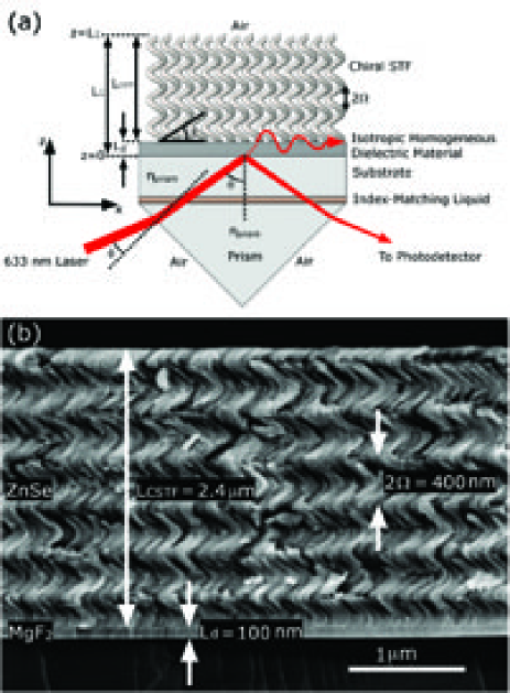
Samples were fabricated by first thermally evaporating an isotropic and homogeneous layer of magnesium fluoride onto a dense flint glass (SF11) substrate (Swiss Jewel Co., Philadelphia, PA, USA) in a custom-made low-pressure chamber. The intended direction of Dyakonov–Tamm-wave propagation was marked by a straight line (the axis in Fig. 1a) on one face of the substrate, and then that face was affixed to the platform face. Then the substrate was shuttered, the chamber was evacuated to a pressure of Torr, and a current that slowly increased to A was passed through a tungsten source boat containing MgF2. The shutter was then removed, and the collimated portion of the MgF2-vapor flux was directed normally towards the substrate which was being rotated at rpm. The current was adjusted manually to maintain a deposition rate of nm s-1, as indicated by the quartz crystal monitor, while the layer of thickness was being deposited. After being left in vacuum for several hours in order to cool, the sample was exposed to atmosphere. Then the substrate was rotated about its surface normal by an offset angle deg, as indicated by parametric simulations [24] to offer the most favorable conditions for the observation of a Dyakanov–Tamm wave. The source boat was then filled with ZnSe, the MgF2-coated substrate was shuttered, the chamber was evacuated to a base pressure of Torr, and the current passing through the source boat was increased slowly to A. The substrate was then reoriented so the collimated portion of the ZnSe-vapor flux would be directed at deg with respect to the substrate plane, a substrate rotation sequence was initiated, and the shutter was removed. The rotation sequence for the deposition of the chiral STF involved discrete steps per revolution while holding the substrate stationary for an interval of s between each movement. As the current manually was adjusted to maintain a deposition rate of nm s-1, a structurally right-handed chiral STF with a structural period nm was deposited. Once the desired final thickness of the chiral STF was achieved, the sample was shuttered, the current passing through the source boat was decreased to A, and the sample was left under vacuum for several hours to cool prior to exposing it to atmosphere. Samples of six different types were made: the magnesium-fluoride layer was either or -nm thick, and the zinc-selenide chiral STF had either , or , or structural periods.
Along with each flint-glass substrate, a silicon wafer was placed on the platform. Thus, the MgF2/ZnSe structure was also deposited on the silicon wafer for the verification of morphology. The silicon wafer was used to avoid troubles caused by charging of the SF11 glass substrate when imaging with a scanning electron microscope (SEM). The wafer with the MgF2/ZnSe structure was immersed in liquid nitrogen and fractured with a punch to reveal a cleaved plane for cross-sectional images to be obtained. Images were obtained for each combination of films on a field-emission SEM (FEI Nova NanoSEM 630, Hillsboro, OR, USA). As an example, the image in Fig. 1b reveals a nm MgF2 layer conjoined with a chiral STF with structural periods, each of thickness nm.
The prism-coupled configuration of Fig. 1a was implemented with a right-angled isosceles prism made of SF11 glass (Edmund Optics, Barrington, NJ, USA). The index-matching fluid had a refractive index of at nm wavelength, as yielded by the Cauchy equation formulated using data supplied by the manufacturer (Cargille Laboratories, Cedar Grove, NJ, USA). The prism/sample combination was then mounted in a commercial device (Metricon 2010/M, Metricon, Pennington, NJ, USA). A -nm wavelength He-Ne laser (CVI Melles-Griot, Albuquerque, NM, USA) was oriented to ensure that the light incident on the prism would be polarized (i.e., the magnetic field of the incident light would be aligned with the axis).
With -polarized light incident on a slanted face of the prism at an angle , the intensity of the light exiting the other slanted face of the prism was measured. The angle of incidence on the MgF2/ZnSe structure was computed as , with . A half-wave plate was then inserted into the beam-path of the incident laser to convert the -polarized light incident on the prism to the -polarized light (i.e., the electric field would be aligned with the axis), and the measurement of the intensity of the exiting light was repeated.
The sample was then removed from the hypotenuse of the prism and the intensity of the light exiting the prism was again measured as a function of for each of the two incident polarization states. Measured values of the ratio were plotted against for all six samples and for both polarization states. This normalization is meaningful, because total internal reflection occurs at the interface of the prism and air for deg.
A sharp dip in the vs. curve is indicative of the excitation of a surface wave, provided its location on the -axis is independent of both and beyond certain threshold values of both parameters [3, 24]. This is reasonable because a surface wave is localized to a specific interface, and increasing the thickness of either partnering material beyond a threshold will not affect the spatial profiles of the fields of a surface wave.
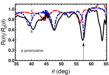
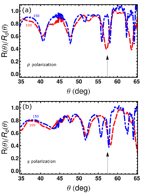
Figure 2 shows vs. curves for when nm. These three curves have a sharp dip in at deg. Aligned dips at deg also occur in Figs. 3a and b for when nm for - and -polarization states, respectively. All of these dips indicate that a surface wave is indeed excited at deg.
The question of which interface is supporting the propagation of the surface wave arises. In the prism-coupled configuration, there are three relevant interfaces. The first interface, between the SF11 substrate and the MgF2 layer, can not support the propagation of a surface wave as there exists no solutions to the dispersion equation for that interface [3, App. C]. The other two relevant interfaces are the MgF2/ZnSe interface and the ZnSe/air interface . A surface wave guided by either of these two interfaces has to be a Dyakonov–Tamm wave, by definition. Thus, Figs. 2 and 3 are proof of the first observation of the Dyakonov–Tamm wave.
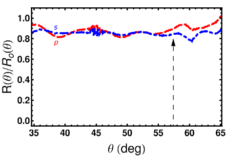
In order to resolve whether the Dyakonov–Tamm wave in Figs. 2 and 3 is guided by the MgF2/ZnSe interface or the ZnSe/air interface, another experiment was conducted. The sample made for this experiment had structural periods of the ZnSe chiral STF, but did not have the MgF2 layer. Because light in the prism is not evanescent when is in a quite large neighborhood of deg, the SF11/ZnSe interface can not guide a Dyakonov–Tamm wave in the prism-coupled experiment conducted with the MgF2-deficient sample. Therefore, any sharp dip at deg in the vs. curve for both polarization states can only be attributed to a Dyakonov–Tamm wave guided by the ZnSe/air interface. Figure 4 shows the results of this experiment which demonstrates, through the absence of a dip near deg, that the ZnSe/air interface did not guide the Dyakonov–Tamm wave observed in the earlier experiments. We concluded that the Dyakonov–Tamm wave observed in Figs. 2 and 3 was guided by the interface of the MgF2 layer (a homogeneous, isotropic dielectric material) and the ZnSe chiral STF (a periodically nonhomogeneous, anisotropic dielectric material).
The experimental observation of the Dyakonov–Tamm wave, confirming theoretical predictions, opens a new avenue in the realm of electromagnetic surface waves. Optical sensing and long-range on-chip communication are among the simpler applications of this new type of surface wave. In particular, as a chiral STF is a porous material that can be infitrated by solutions of analytes, application for optical sensing should follow shortly. High sensitivity is expected because the Dyakonov–Tamm wave is expected to propagate over long distances due to the absence of non-dissipative partnering materials (such as metals) and thus have a large interaction volume. Furthermore, as multiple modes of Dyakonov–Tamm wave propagation are possible at the same frequency [27], multi-analyte sensing may be possible, with proper selection of the partnering materials.
References
- [1] A. D. Boardman, ed., Electromagnetic Surface Modes (Wiley, 1982).
- [2] D. Sarid and W. Challener, Modern Introduction to Surface Plasmons: Theory, Mathematica Modeling and Applications (Cambridge University Press, 2010).
- [3] J. A. Polo Jr., T. G. Mackay, and A. Lakhtakia, Electromagnetic Surface Waves: A Modern Perspective (Elsevier, 2013).
- [4] J. Homola, ed., Surface Plasmon Resonance Based Sensors (Springer, 2006).
- [5] M. Shinn and W. M. Robertson, Sens. Actuat. B: Chem. 105, 360 (2005).
- [6] V. N. Konopsky and E. V. Alieva, Anal. Chem. 79, 4729 (2007).
- [7] S. E. Swiontek, D. P. Pulsifer, and A. Lakhtakia, Sci. Rep. 3, 1409 (2013).
- [8] E. Yeatman and E. A. Ash, Electron. Lett. 23, 1091 (1987)
- [9] H. A. Atwater and A. Polman, Nature Mater. 9, 205 (2010).
- [10] J. S. Sekhon and S. S. Verma, Curr. Sci. India 101, 484 (2011).
- [11] R. H. Ritchie, Phys. Rev. 106, 874 (1957).
- [12] T. Turbadar, Proc. Phys. Soc. 73, 40 (1959).
- [13] A. Otto, Z. Phys. 216, 398 (1968).
- [14] E. Kretschmann and H. Raether, Z. Naturforsch. A 23, 2135 (1968).
- [15] P. Berini, Adv. Opt. Photon. 1, 484 (2009).
- [16] P. Yeh, A. Yariv, and C.-S. Hong, J. Opt. Soc. Am. 67, 423 (1977).
- [17] I. Tamm, Z. Phys. A 76, 849 (1932).
- [18] P. Yeh, A. Yariv, and A. Y. Cho, Appl. Phys. Lett. 32, 104 (1978).
- [19] V. N. Konopsky, T. Karakouz, E. V. Alieva, C. Vicario, S. K. Sekatskii, and G. Dietler, Sensors 13, 2566 (2013).
- [20] M. I. D’yakonov, Sov. Phys. JETP 67, 714 (1988).
- [21] O. Takayama, L. Crasovan, D. Artigas, and L. Torner, Phys. Rev. Lett. 102, 043903 (2009).
- [22] O. Takayama, L.-C. Crasovan, S. K. Johansen, D. Mihalache, D. Artigas, and L. Torner, Electromagnetics 28, 126 (2008).
- [23] A. Lakhtakia and J. A. Polo Jr., J. Eur. Opt. Soc.–Rapid Publ. 2, 07021 (2007).
- [24] D. P. Pulsifer, M. Faryad, and A. Lakhtakia, J. Opt. Soc. Am. B 30, 2081 (2013).
- [25] A. Lakhtakia and R. Messier, Sculptured Thin Films: Nanoengineered Morphology and Optics (SPIE Press, 2005).
- [26] Simulation has shown that the use of a non-integer ratio will periodically shift the value of at which a Dyakonov–Tamm wave will be observed [24]. This ratio should be an integer for unambiguous results.
- [27] M. Faryad and A. Lakhtakia, Opt. Commun. 294, 192 (2013).