ICFO]ICFO - Institut de Ciencies Fotoniques, Mediterranean Technology Park, 08860 Castelldefels (Barcelona), Spain \altaffiliationICREA - Institució Catalana de Recerca i Estudis Avançats, Barcelona, Spain
Multiple Excitation of Confined Graphene Plasmons by Single Free Electrons
Abstract
We show that free electrons can efficiently excite plasmons in doped graphene with probabilities of order one per electron. More precisely, we predict multiple excitations of a single confined plasmon mode in graphene nanostructures. These unprecedentedly large electron-plasmon couplings are explained using a simple scaling law and further investigated through a general quantum description of the electron-plasmon interaction. From a fundamental viewpoint, multiple plasmon excitations by a single electron provides a unique tool for exploring the bosonic quantum nature of these collective modes. Our study does not only open a viable path towards multiple excitation of a single plasmon mode by single electrons, but it also reveals graphene nanostructures as ideal systems for producing, detecting, and manipulating plasmons using electron probes.
KEYWORDS: graphene, plasmons, multiple plasmon excitation, electron energy loss, quantum plasmonics, nanophotonics
The existence of surface plasmons was first demonstrated by observing energy losses produced in their interaction with free electrons 1, 2. Following those pioneering studies, electron beams have revealed many of the properties of plasmons through energy-loss and cathodoluminescence spectroscopies, which benefit from the impressive combination of high spatial and spectral resolutions that is currently available in electron microscopes and that allows mapping plasmon modes in metallic nanoparticles and other nanostructures of practical interest 3, 4, 5. However, plasmon creation rates are generally low, thus rendering multiple excitations of a single plasmon mode by a single electron extremely unlikely.
From a fundamental viewpoint, the question arises, what it the maximum excitation probability of a plasmon by a passing electron? This depends on a number of parameters, such as the interplay between momentum and energy conservation during the exchange with the electron, the spatial extension of the electromagnetic fields associated with the electron and the plasmon, and the interaction time, which are in turn controlled by the spatial extension of the excitation and the speed of the electron. One expects that highly confined optical modes, encompassing a large density of electromagnetic energy, combined with low-energy electrons, which experience long interaction times, provide an optimum answer to this question. This intuition is corroborated here by examining the interaction between free electrons and graphene plasmons. The peculiar electronic structure of this material leads to the emergence of strongly confined plasmons (size of the light wavelength) when the carbon layer is doped with charge carriers 6, 7, 8, 9, 10. Graphene plasmons have been recently observed and their electrical modulation unambiguously demonstrated through near-field spatial mapping 11, 12, 13 and far-field spectroscopy 14, 15, 16. These low-energy plasmons, which appear at mid-infrared and lower frequencies, should not be confused with the higher-energy and plasmons that show up in most carbon allotropes, and that have been extensively studied through electron energy-loss spectroscopy (EELS) in fullerenes 17, 18, nanotubes 19, and graphene 20, 21, 22, 23. These high-energy plasmons are not electrically tunable. We thus concentrate on electrically driven low-energy plasmons in graphene. Despite their potential for quantum optics and light modulation 24, 25, 26, the small size of the graphene structures relative to the light wavelength (see below) poses the challenge of controlling their excitation and detection with suitably fine spatial precision. Using currently available subnanometer-sized beam spots, free electrons appear to be a viable solution to create and detect graphene plasmons with large yield and high spatial resolution. As a first step in this direction, angle-resolved EELS performed with low-energy electrons has been used to map the dispersion relation of low-energy graphene plasmons 27, 28, as well as their hybridization with the phonons of a SiC substrate 29, although this technique has limited spatial resolution.
The probabilities of multiple plasmon losses, as observed in EELS 30 and photoemission 31 experiments, are well known to follow Poisson distributions 32, 33, 18. Previous studies have concentrated on plasmon bands, where the electrons simultaneously interact with a large number of plasmon modes. We are instead interested in the interaction with a spectrally isolated single mode.
In this article, we show that a single electron can generate graphene plasmons with large yield of order one. We discuss the excitation of both propagating plasmons in extended carbon sheets and localized plasmons in nanostructured graphene. The excitation probability is shown to reach a maximum value when the interaction time is of the order of the plasmon period. Our results suggest practical schemes for the excitation of multiple localized graphene plasmons using electron beams, thus opening new perspectives for the observation of nonlinear phenomena at the level of a few plasmons excited within a single mode of an individual graphene structure by a single electron.
1 RESULTS AND DISCUSSION
Plasmon excitation in extended graphene. Before discussing confined plasmons, we explore analytical limits for electrons interacting with a homogeneous graphene layer. The dispersion relation of free-standing graphene plasmons can be directly obtained from the pole of the Fresnel coefficient for polarization 7, which in the electrostatic limit reduces to
| (1) |
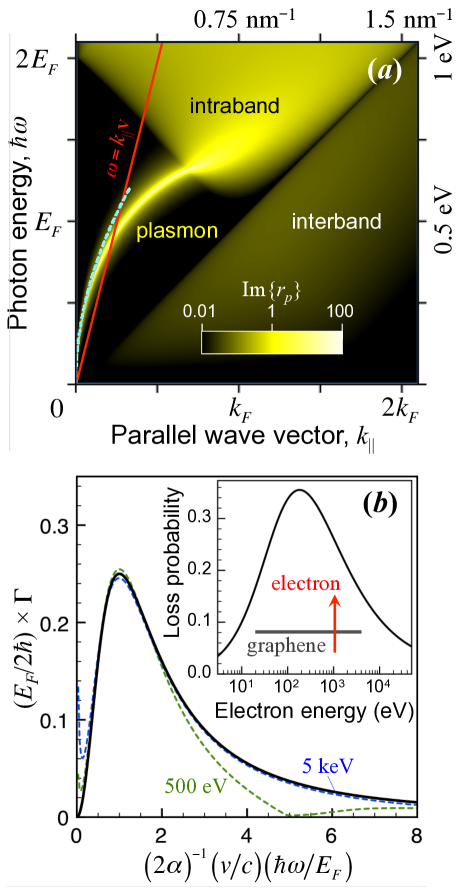
Here, is the conductivity, and and are the light parallel wave-vector and frequency. Because of the translational invariance of the carbon layer, the full dependence of the conductivity can be directly incorporated in 1 to account for nonlocal effects, which include the excitation of electron-hole pairs. The dispersion diagram of 1a, which shows calculated in the random-phase approximation 34, 35 (RPA) under realistic doping conditions (Fermi energy eV, corresponding to a carrier density cm-2, where m/s is the Fermi velocity), reveals a plasmon band as a sharp feature outside the regions occupied by intra- and interband electron-hole-pair transitions. We justify the use of the electrostatic approximation to describe the response of graphene because the plasmon wavelength is much smaller than the light wavelength (e.g., the Fermi wavelength is nm, which is 300 times smaller than the light wavelength at an energy eV).
Under these conditions, an electron crossing the carbon sheet with constant normal velocity has a probability 5
| (2) |
of lossing energy (see Methods for more details). Likewise, an electron moving along a path length parallel to the graphene experiences a loss probability (see Methods)
| (3) |
where is the distance between graphene and the electron. These probabilities are determined by , which is represented in 1a. Clearly, losses around the region are favored.
It is instructive to evaluate LABEL:Gperp,Gpara using the Drude model for the graphene conductivity 7
| (4) |
where is a phenomenological decay time. The latter determines the plasmon quality factor , as measured in recent experiments 12, 11, 15, 16, 13. This model works well for photon energies below the Fermi level (), but neglects interband transitions that take place at higher energies. In the limit, we can approximate
where
| (5) |
is the plasmon wave vector (broken curve in 1a). Using this approximation in LABEL:Gperp,Gpara, the plasmon contribution to the loss probability reduces to
| (6) |
where
and is the fine-structure constant. For a perpendicular trajectory, 6 has a maximum at (1b). Its integral over the region, in which the plasmon is well defined, shows a maximum probability for an electron energy eV when we take eV. This is an unusually high plasmon yield for electrons traversing a thin film. However, this probability is spread over a continuum of 2D plasmons. In what follows, we concentrate on localized plasmons in finite graphene islands, which feature instead a discrete spectrum, thus placing the entire electron-plasmon strength on a few modes, and consequently, increasing the probability for a single electron to excite more than one plasmon in a single mode.
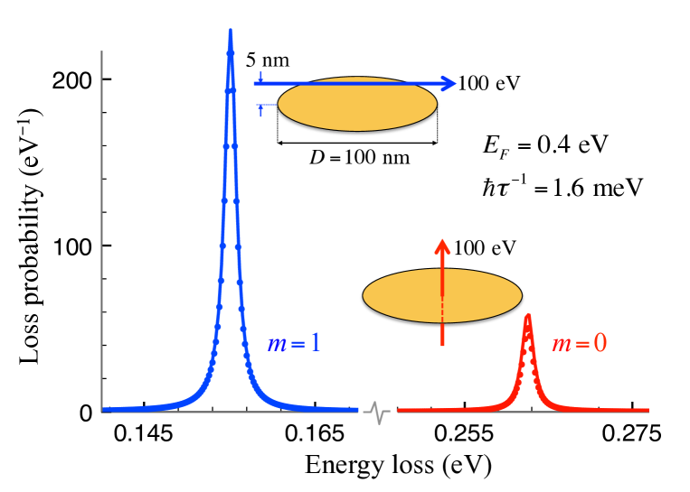
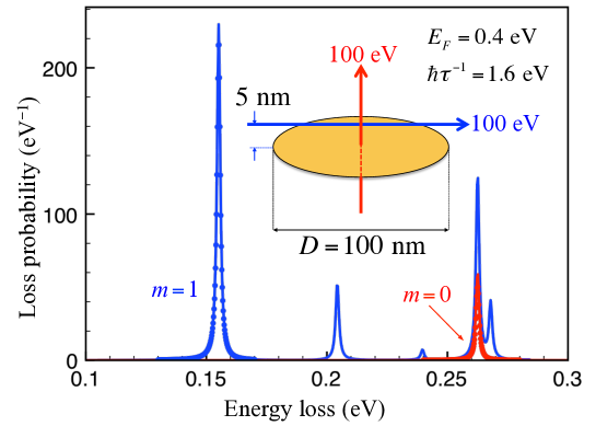
Plasmon excitation in graphene nanostructures. Doped graphene nanoislands can support plasmons, as recently observed through optical absorption measurements 15, 16. For small islands, the concentration of electromagnetic energy that characterizes these plasmons is extremely high, therefore producing strong coupling with nearby quantum emitters 9. Likewise, the interaction of localized plasmons with a passing electron is expected to be particularly intense. This intuition is put to the test in 2, where we consider a 100 eV electron interacting with a 100 nm graphene disk doped to a Fermi energy eV. We calculate the electron energy-loss probability using classical electrodynamics 5, assuming linear response, and describing the graphene through the Drude conductivity of 4, which we spread over a thin layer of nm thickness, as prescribed elsewhere 9. We investigate both a parallel trajectory, with the electron passing 5 nm away from the carbon sheet, and a perpendicular trajectory, with the electron crossing the disk center. 2 only shows the lowest-energy mode that is excited for each of these geometries, corresponding to and azimuthal symmetries, respectively. An overview of a broader spectral range (see Methods, 7) reveals that these modes are actually well isolated from higher-order spectral features within each respective symmetry. Because we use the Drude model, the width of the plasmon peaks in 2 coincides with (see below), which is set to 1.6 meV, or equivalently, we consider a mobility of cmV s, which is a moderate value below those measured in suspended 36 and BN-supported 37 high-quality graphene.
The area of the plasmon peaks is a -independent, dimensionless quantity that corresponds to the number of plasmons excited per incident electron. For the mode (parallel trajectory), we find plasmons per electron. This leads us to the following two important conclusions: (i) the probability of multiple plasmon generation is expected to be significant, and its study requires a quantum treatment of the plasmons to cope with the bosonic statistics of these modes, as described below; and (ii) linear response theory, which we assume within the classical electromagnetic calculations shown in 2, is no longer valid because nonlinear and quantum corrections become substantial. These two conclusions are further explored in what follows, but first we discuss a universal scaling law for the energy-loss probability that is also relevant to the description of multiple plasmon processes.
Electrostatic scaling law and maximum plasmon excitation rate. In electrodynamics, the light wavelength introduces a length scale that renders the solution of specific geometries size dependent. In contrast, electrostatics admits scale-invariant solutions, which have long been recognized to provide convenient mode decompositions, particularly when studying electron energy losses 38, 39, 40. Modeling graphene as an infinitely thin layer, its electrostatic solutions take a particularly simple form 15. We provide a comprehensive derivation of the resulting scaling laws in the Methods section, the main results of which are summarized next. We focus on a spectrally isolated plasmon of frequency sustained by a graphene nanoisland of characteristic size (e.g., the diameter of a disk) and homogeneous Fermi energy .
Assuming the Drude model for the graphene conductivity (4), the plasmon frequency is found to be
| (7) |
where is a dimensionless, scale-invariant parameter that only depends on the nanoisland geometry and plasmon symmetry under consideration (see 31). In particular, we have for the lowest-order axially symmetric plasmon of a graphene disk ( azimuthal symmetry), which is the lowest-frequency mode excited by an electron moving along the disk axis. Also, we find for the lowest-order mode, which can be excited in asymmetric configurations. It is important to stress that 7 reveals a linear dependence of on .
Furthermore, the average number of plasmons excited by the electron (i.e., the plasmon yield) reduces to (see Methods, LABEL:Gj,Pj)
| (8) |
within this classical theory. Here, we have defined the two dimensionless parameters
| (9a) | |||
| (9b) |
as well as the dimensionless loss function
| (10) |
The integral is over the electron path length in units of , whereas is the dimensionless scaled plasmon electric potential defined in 36, which is calculated once and for all following the procedure explained in the Methods section (see 39 and beyond).
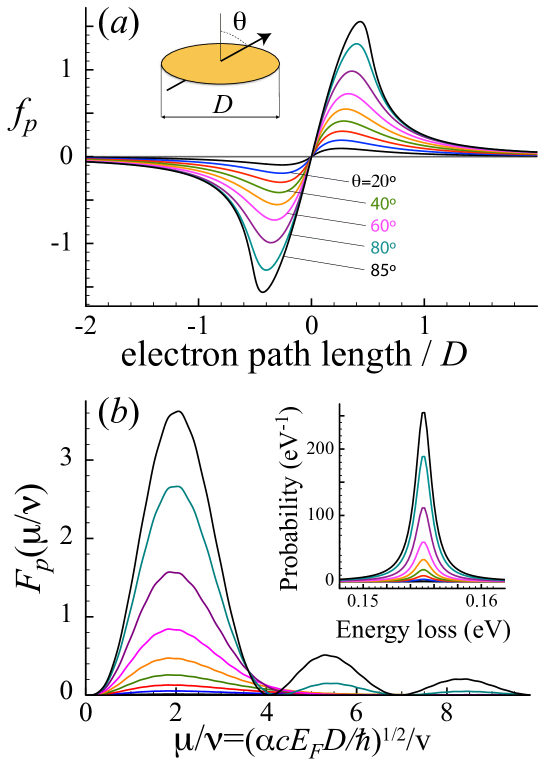
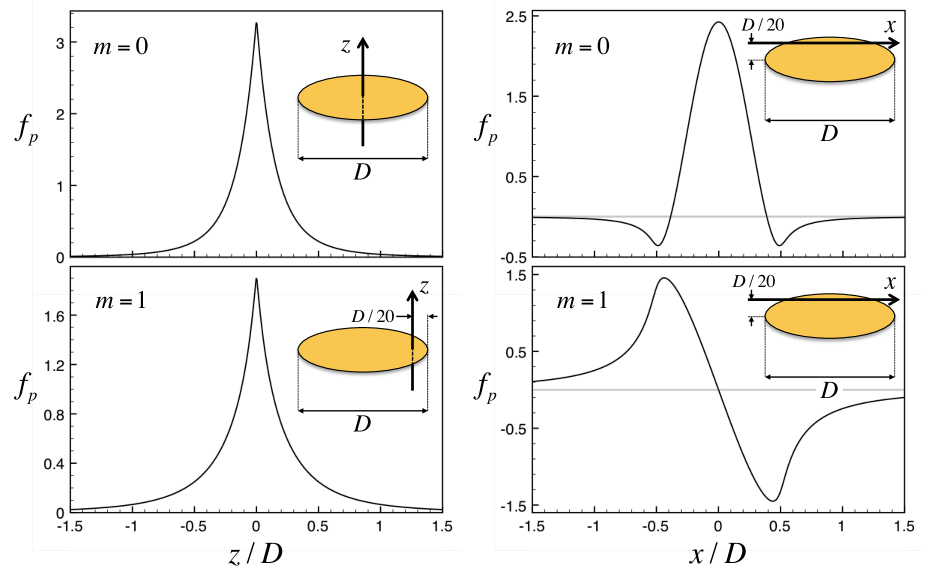
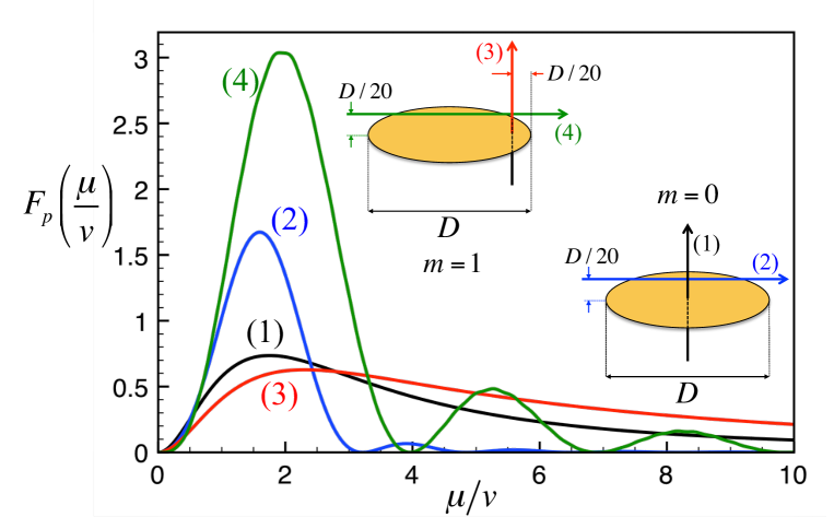
We show characteristic examples of and in 3 for electrons crossing the center of a graphene disk following different oblique trajectories. As is proportional to the electrostatic potential associated with the plasmon, it is a real function of position. For the mode considered in 3, vanishes at the axis of rotational symmetry and takes large values near the disk edges, leading to antisymmetric dip-peak patterns (3a). The resulting loss function (3b) exhibits oscillations depending on the relative phase with which the potential is sampled along the electron trajectory (see 10). As anticipated above, this depends on the path length traveled by the electron during an optical plasmon period () relative to the extension of the plasmon (), the ratio of which is precisely . When exciting symmetric plasmon modes (e.g., ), non-oscillating profiles are obtained, equally characterized by maxima exceeding 1 at for electrons passing at a small distance from the disk (see Supplementary Information, SI).
For a relatively grazing trajectory (), a maximum plasmon excitation probability is reached for an electron velocity (see 3b). As an indicative value, for a disk of diameter nm doped to a Fermi energy eV, similar to those fabricated in recent experiments 15, which can sustain plasmons of eV energy, the maximum excitation probability is and is obtained using eV electrons. These magnitudes can be readily computed for other disk size and doping conditions via the scaling laws for the plasmon frequency (7), the maximum excitation probability , and the electron energy . Although arbitrarily large values of can be in principle achieved through reducing and (even while maintaining their ratio constant, and consequently, also ) the graphene size is limited to nm, as plasmons in smaller islands are strongly quenched by nonlocal effects 41. With nm and eV, we have eV plasmons that can be excited by 9 eV electrons with probability per incident electron. This result is clearly outside the range of validity of linear response theory and clearly anticipates large multiple-plasmon excitation probabilities.
Quantum mechanical description. The above classical formalism follows a long tradition of explaining electron energy-loss spectra within classical theory,5 under the assumption that the total excitation rate is small (i.e., ), thus rendering multiple plasmon excitations highly unlikely. This is inapplicable to describe electron-driven plasmon generation in graphene, for which we can have . Therefore, a quantum treatment of the plasmons becomes necessary. We follow a similar approach as in previous studies of multiple plasmon losses 32, 33, 18, here adapted to deal with a single plasmon mode. Describing the electron as a classical external charge density and the plasmon as a bosonic mode, we consider the Hamiltonian
| (11) |
where the operator () annihilates (creates) a plasmon of frequency , and the time-dependent coupling coefficient is defined as
| (12) |
in terms of , the electric potential associated with the plasmon. In the electrostatic approximation, neglecting the effect of inelastic plasmon decay, it is safe to assume that is real. Notice that is just the electrostatic energy subtracted or added to the system when removing or creating one plasmon (i.e., the integral represents the potential energy of the external charge in the presence of the potential created by one plasmon). The Hamiltonian should be realistic under the condition that both the electron-plasmon interaction time and the optical cycle are small compared with the plasmon lifetime. In practice, this means that the electron behaves a point-like particle, or at least, its wave function is spread over a region of size . Additionally, we assume the electron kinetic energy to be much larger than the plasmon energy, so that multiple plasmon excitations do not significantly change the electron velocity (non-recoil approximation).
As the plasmon state evolves under the influence of a linear term in 11 with a classical coupling constant , it should exhibit classical statistics 42. Indeed, it is easy to verify that the plasmon wave function
| (13) |
is a solution of Schrödinger’s equation , where
| (14) |
is a coherent state 43 with
whereas
is an overall phase that does not affect the plasmon-number distribution. The average number of plasmons excited at a given time is given by . We thus conclude that the probability of exciting plasmons simutaneoulsy follows a Poissonian distribution
| (15) |
which yields a second-order correlation .
Expressing and in terms of , noticing that (i.e., no plasmons present before interaction with the electron), and using a similar scaling as in the classical theory discussed above, we can write the probability of exciting plasmons as
| (16) |
where is the classical linear probability given by 8, which coincides with the average number of excited plasmons per electron, , and can take values above 1.
Inclusion of plasmon losses. Inelastic losses during the electron-plasmon interaction time have been so far ignored in the above quantum description. However, for sufficiently slow electrons or very lossy plasmons, the interaction time can be comparable to the plasmon lifetime , so that the above quantum formalism needs to be amended, for example by following the time evolution of the density matrix , according to its equation of motion 44
| (17) |
where the Hamiltonian is defined by LABEL:H,gt. The solution to this equation can still be given in analytical form:
| (18) |
where is again a coherent state (see 14), but we have to redefine
| (19) |
It is straightforward to verify that LABEL:xixi,newxi are indeed a solution of 17.
A simultaneous density-matrix description of the electron and plasmon quantum evolutions involves a larger configuration space that is beyond the scope of this paper. We can however argue that the probabilities corresponding to the electron lossing energies must still follow a Poissonian distribution if we trace out the plasmon mode. At , all plasmons must have decayed, so that we can obtain the average number of plasmon losses from the time integral of the total plasmon decay rate, . Again, we find that this quantity coincides with the classical linear loss probability , which is now given by
where is the time-Fourier transform of . This expression reduces to (i.e., 8) in the limit of high plasmon quality factor .
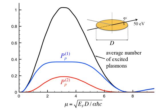
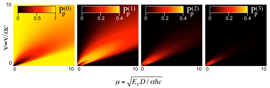
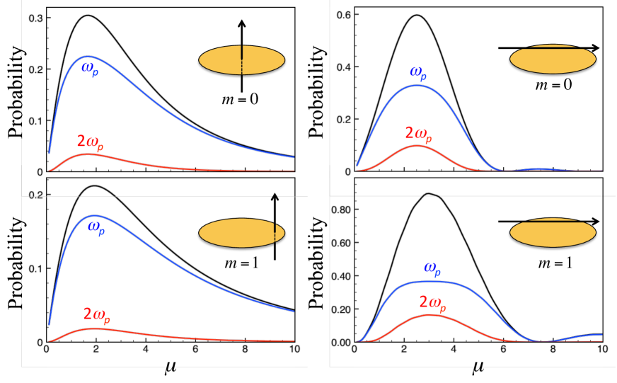
Multiple plasmon generation by a single electron. We show in 4 results obtained by solving 16 under the conditions of the most grazing trajectory from those considered in 3. In particular, the electron energy is 50 eV, which corresponds to . The average number of plasmons excited by a single electron under these conditions reaches a maximum value slightly above 1, distributed in a probability of exciting only one plasmon, a probability of simultaneously exciting two plasmons, and lower probabilities of generating more than two plasmons. The peak maximum is observed at (this corresponds for example to nm and eV), which leads to , slightly to the left of the main peak observed within linear theory at in 3.
The full dependence of the probability of generating plasmons on and is shown in 5. For large , the results approach the linear regime, only single plasmons are effectively excited, and the highest probability is peaked around a broad region centered along the line. At small ’s, a more complex behavior is observed. The double-plasmon excitation probability is above 20% over a broad range of ’s, and even the probability of simultaneously generating three plasmons takes significant values up to . The probability is increasingly more confined towards the low and region when a larger number of plasmons is considered. Notice however the presence of a dip in that region for single-plasmon excitation, which is due to transits towards a larger numbers of plasmons created. A similar effect is observed for at even lower values of and .
2 CONCLUSIONS AND OUTLOOK
We predict unprecedentedly high graphene-plasmon excitation rates by relatively low-energy free electrons. When a plasmon is highly confined down to a small size compared with the light wavelength, the dipole moment associated with the plasmon is small and this limits the strength of its coupling to light. Direct optical excitation becomes inefficient, and one requires near-field probes to couple to the plasmons 11, 12. In fact electrons act as versatile near-field probes that can be aimed at the desired sample region. Furthermore, electrons carry strongly evanescent electromagnetic fields that couple with high efficiency to confined optical modes, thus rendering the observation of multiple plasmon excitation feasible. Our calculations show double excitation of a single plasmon mode with efficiencies of up to 20% per incident electron in graphene structures with similar size and doping levels as those produced in recent experiments 15.
Besides its fundamental interest, multiple plasmon excitation is potentially useful to explore nonlinear optical response at the nanoscale. In particular, quantum nonlinearities at the single- or few-plasmon level has been predicted in small graphene islands 45. As the excitation of strongly confined plasmons by optical means remains a major challenge, free electrons provide the practical means to explore this exotic quantum behavior. In particular, the generation of plasmons by a single electron produces an energy loss , the detection of which can be used to signal the creation of a plasmon-number state in the graphene island.
The electron energies for which plasmon excitation probabilities are high lie in the sub-keV range, which is routinely employed in low-energy EELS studies 46, as already reported for collective excitations in graphene 27, 29. In practice, one could study electrons that are elastically (and specularly) reflected on a patterned graphene film. Actually, the analysis of energy losses in reflected electrons was already pioneered in the first observation of surface plasmons in metals 2. A similar approach could be followed to reveal multiple graphene plasmon excitations by individual electrons. Incidentally, low-energy electron diffraction at the carbon honeycomb lattice could provide additional ways of observing these excitations through elastically diffracted beams, for which plasmons should be the dominant channel of inelastic losses. Inelastic losses in core-level photoelectrons, which have been used to study plasmons in semi-infinite 47, 31 and ultrahin 48 metals, as well as (the so-called plasmon satellites), offer another alternative to resolve multiple plasmon excitations in confined systems.
In practical experiments, the graphene structures are likely to lie on a substrate, and their size and shape must be chosen such that the energies of higher-order plasmons are not multiples of the targeted plasmon energy. Although for the sake of simplicity the analysis carried out here is limited to self-standing graphene structures, it can be trivially extended to carbon islands supported on a substrate of permittivity by simply multiplying both the graphene conductivity (or equivalently, the Fermi energy in the Drude model) and the external electron potential by a factor . This factor incorporates a rigorous correction to the free-space point-charge Coulomb interaction when the charge is instead placed right at the substrate surface. Likewise, the contribution of the image potential leads to a total external potential at the surface given by times the bare potential of the moving electron. The presence of a surface can however attenuate the transmitted electron intensity, so reflection measurements appear as a more suitable configuration. It should be emphasized that the energy loss and plasmon excitation probabilities produced by transmitted electrons coincide with those for specularly reflected electrons, and therefore, the present theory is equally applicable to reflection geometries, as indicated in 4. This is due to the small thickness of the graphene, where induced charges cannot provide information on which side the electron is coming from. A detailed analysis consisting in using an external electron charge for a specularly reflected electron fully confirms this result.
High plasmon excitation efficiencies should be also observable in metal nanoparticles. One could for example study electrons reflected on a monolayer of nanometer-sized gold colloids, which present a similar degree of mode confinement as graphene. However, plasmons in noble metals have lower optical quality factors than in graphene, thus compromising the condition that be smaller than the electron wave function spread (see above). Additionally, the trajectories of sub-keV electrons reflected from metal colloids can be dramatically affected by their stochastic distributions of facets and small degree of surface homogeneity compared with graphene, the 2D morphology of which can be tailored with nearly atomic detail 49.
In summary, graphene provides a unique combination of surface quality, tunability, and optical confinement that makes the detection of multiple plasmon excitations by individual electrons feasible, thus opening a new avenue to explore fundamental quantum phenonema, nanoscale optical nonlinearities, and efficient mechanisms of plasmon excitation and detection with potential application to opto-electronic nanodevices.
3 METHODS
In this section, we formulate an electrostatic scaling law and a quantum-mechanical model that allow us to describe multiple excitations of graphene plasmons by fast electrons. The model agrees with classical theory within first-order perturbation theory, and provides a fast, accurate procedure to compute excitation probabilities for a wide range of electron velocities and graphene parameters.
Eigenmode expansion of the classical electrostatic potential near graphene. The graphene structures under consideration are much smaller than the light wavelengths associated with their plasmon frequencies, and therefore, we can describe their response in the electrostatic limit. The optical electric field can be thus expressed as the gradient of an electric potential in the plane of the graphene. It is convenient to write the self-consistent relation
| (20) |
where the integral represents the potential produced by the charge density induced on the graphene, which in virtue of the continuity equation, is in turn expressed as in terms of the induced current . Here, is the 2D graphene conductivity, which we assume to act locally. These expressions involve coordinate vectors in the plane of the graphene, . Although 20 is valid for any point , we take to obtain the self-consistent electric potential in the graphene sheet. Incidentally, the abrupt change of at the edge of a graphene structure produces a divergent boundary contribution to the integrand of 20. These types of divergences have been extensively studied in the context of magneplasmons at the edge of a bounded 2D electron gas 50, and more recently also in graphene 51. In practice, we can solve 20 numerically by smoothing the edge (e.g., though in-plane modal expansions of and ). This produces convergent results in agreement with direct solutions of the 3D Poisson equation. However, we only use 20 in this article to derive formal relations and scaling laws involving plasmon modes, whereas specific numerical computations are performed following a different method, as explained below.
Given the lack of absolute length scales in electrostatics, we can recast 20 in scale-invariant form by using the reduced 2D coordinate vectors , where is a characteristic length of the graphene structure (e.g., the diameter of a disk). Additionally, we assume that the conductivity can be separated as . For homogeneously doped graphene, simply represents a filling factor that takes the value in the graphene and vanishes elsewhere. However, the present formalism can be readily applied to more realistic inhomogeneous doping profiles by transferring the space-dependence of to . This can be applied to describe inhomogeneously doped graphene, including divergences in the doping density near the edges 52. Combining these elements, we obtain
| (21) |
where
| (22) |
is a dimensionless parameter containing all the physical characteristics of the graphene, such as the doping level, the temperature dependence, and the rate of inelastic losses, as well as the dependence on frequency . Integrating by parts and taking the in-plane 2D gradient on both sides of 21, we find the more symmetric expression
| (23) |
where and
is a symmetric matrix that is invariant under exchange of its arguments: . This implies that is a real, symmetric operator that admits a complete set of real eigenvalues and orthonormalized eigenvectors satisfying
and
where is the unit matrix.
The solution to 23 can be expressed in terms of these eigenmodes as
with expansion coefficients
| (24) |
The potential outside the graphene can be constructed from through the induced charge . Following a procedure similar to the derivation of 21, we find
| (25) |
where
| (26) |
and we have defined the reduced 3D coordinate vector .
Classical screened interaction potential. The screened interaction is defined as the potential produced at by a unit point charge placed at and oscillating in time as . We use the formalism introduced in the previous paragraph and consider in 24 the point-charge external potential . Integrating by parts, we find (see 26), which upon insertion into 25 yields
| (27) |
The well-known symmetry is apparent in 27. For an arbitrary external charge distribution , which we express in frequency space as
| (28) |
the induced potential can be written using the screened interaction as
| (29) |
Electrostatic scaling law for the plasmon frequency. The condition determines a plasmon frequency of the system for a specific eigenstate , subject to the condition (see below). This relation has general validity within the electrostatic limit, so that all the graphene characteristics, including the size of the structure , are fully contained within , and thus, given a certain shape (e.g., a disk), the eigenvalues can be calculated once and for all to obtain the plasmon frequency for arbitrary size or doping.
A powerful electrostatic law can be formulated by assuming the Drude model for the conductivity of graphene (4). The plasmon frequency is then given by , where
| (30) |
and we have defined the real number (provided )
| (31) |
to obtain the rightmost expression in 30.
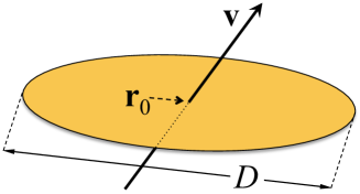
Classical approach to the electron energy-loss probability. We consider an electron moving with constant velocity vector along the straight-line trajectory passing near or through a graphene structure, as shown in 6. The energy transferred from the electron to the graphene () can be written as 5
where
| (32) |
is the loss probability per unit of frequency range, and is the component of the potential induced by the electron along its path. The external charge density associated with the moving electron reduces to . Using this expression together with LABEL:W,rhow,Wrho,P, the loss probability is found to be
| (33) |
where ,
| (34) |
we adopt the notation , and the integral is over the path length (in units of ) along the velocity vector direction.
We now concentrate on a specific plasmon resonance and neglect contributions to the loss probability arising from modes other than this particular one. For simplicity, we work within the Drude model and assume a small plasmon width . Using LABEL:eta,Drude in 33, and integrating over to cover the plasmon peak area, we find
| (35) |
for the probability of exciting plasmon by the incident electron. Finally, we can recast 35 into the scale-invariant form of 8, using the definitions of LABEL:munu,Fpxi, and further defining the dimensionless scaled plasmon electric potential
| (36) |
We show in 7 two examples of loss spectra for 100 eV electrons passing near a 100 nm graphene disk. The lowest-energy plasmon features for both and symmetries are clearly separated from other peaks in their corresponding spectral regions, thus justifying the approximation of 35. We further compare in this figure the full solution of Maxwell’s equations (solid curves) with the result obtained from 33 using a single plasmon term for each of the lowest-order and modes, with and , respectively, and with calculated from the plasmon potential, which is normalized as explained below.
Quantum approach to the screened interaction potential. The linear screened interaction potential can be obtained by solving the density matrix (17), which yields the solution , with given by LABEL:psichi,newxi. Expressing in frequency space , we can then write
where is defined by 28. Now, calculating the induced potential from its expectation value
we find
(or equivalently, 29), where
| (37) |
is the quantum-mechanical counterpart of 27.
Normalization of the plasmon potential. In the Drude model (4), assuming a dominant plasmon mode contributing to the response with frequency given by 7, we find that LABEL:W,WQM are identical under the assumption , provided we take
| (38) |
where is the dimensionless scaled plasmon electric potential defined by 36, which is independent of the doping level and the size of the structure . As a self-consistency test, we calculate the plasmon excitation probability to first-order perturbation from the quantum model, which yields
| (39) |
Indeed, this equation coincides with the classsical result of 35, provided 38 is satisfied.
In practice we obtain the plasmon potential as follows: first, we calculate the potential induced by a dipole placed near the graphene and oscillating at frequency using the boundary-element method 53 (BEM) for fixed values of and ; the resulting potential must be equal to times an unknown constant; we deduce this constant by calculating the plasmon excitation probability from 39 and by comparing the result to a well-established classical calculation of the loss probability based upon BEM 5; finally, we use the scaling laws of LABEL:wp,phivarphi to obtain and for any desired values of and , assuming the validity of the Drude model. We have verified that this procedure yields, within the accuracy of the BEM method, the same scaled potentials and for different initial values of and . Incidentally, once is calculated, 39 provides a fast way of obtaining loss probabilities for arbitrary values of the electron velocity, the size of the structure, and the doping conditions.
Analytical expressions for the electron energy-loss probability in homogeneous graphene. In the electrostatic limit, the loss probability of electrons moving either parallel or perpendicularly with respect to an extended sheet of homogeneously doped graphene can be expressed in terms of the Fresnel reflection coefficient for polarized light, as shown in LABEL:Gperp,Gpara. Indeed, for a parallel trajectory, we can readily use the well-established dielectric formalism (e.g., Eq. (25) of Ref. 5 in the limit), which directly yields 3. Likewise, for a perpendicular trajectory, we can write the bare potential of the moving electron in space as
Inserting this expression into 20 and writing the 2D Coulomb interaction as , we find the induced potential
which, together with 32, allows us to write the loss probability for a perpendicular trajectory as shown in 2. It should be noted that the external field produced on the graphene by an electron that is specularly reflected at the graphene plane is also given by the above expression for , and consequently, 2 yields the loss probability for such reflected trajectory as well.
4 Supporting Information
We provide further examples of the normalized functions and , as well as multiple plasmon excitations for parallel and perpendicular trajectories with respect to a doped graphene disk.
Examples of the normalized functions and for a disk and different electron trajectories are offered in Figs. 8 and 9. The highest probability among the trajectories considered in these figures is , which is obtained in the excitation of the mode with for an electron moving parallel to the graphene surface. With a characteristic doping eV and a disk diameter nm, we have , and the excitation peak occurs for , or equivalently, for an electron energy eV. The plasmon energy (see main paper) is eV. The electron passes at a distance nm from the graphene (see Fig. 9, upper inset). The excitation probability is then 73%, which reveals a clear departure from the perturbative regime, and thus this configuration requires a more detailed analysis including multiple-plasmon excitation.
5 Acknowledgement
The author acknowledges helpful and enjoyable discussions with Archie Howie and Darrick E. Chang. He also thanks IQFR-CSIC for providing computers used for numerical simulations. This work has been supported in part by the Spanish MEC (MAT2010-14885) and the EC (Graphene Flagship CNECT-ICT-604391).
References
- Ritchie 1957 Ritchie, R. H. Plasma Losses by Fast Electrons in Thin Films. Phys. Rev. 1957, 106, 874–881
- Powell and Swan 1959 Powell, C. J.; Swan, J. B. Origin of the Characteristic Electron Energy Losses in Aluminum. Phys. Rev. 1959, 115, 869–875
- Nelayah et al. 2007 Nelayah, J.; Kociak, M.; O. Stéphan,; García de Abajo, F. J.; Tencé, M.; Henrard, L.; Taverna, D.; Pastoriza-Santos, I.; Liz-Marzán, L. M.; Colliex, C. Mapping Surface Plasmons on a Single Metallic Nanoparticle. Nat. Phys. 2007, 3, 348–353
- Rossouw et al. 2011 Rossouw, D.; Couillard, M.; Vickery, J.; Kumacheva, E.; Botton, G. A. Multipolar Plasmonic Resonances in Silver Nanowire Antennas Imaged with a Subnanometer Electron Probe. Nano Lett. 2011, 11, 1499–1504
- García de Abajo 2010 García de Abajo, F. J. Optical Excitations in Electron Microscopy. Rev. Mod. Phys. 2010, 82, 209–275
- Castro Neto et al. 2009 Castro Neto, A. H.; Guinea, F.; Peres, N. M. R.; Novoselov, K. S.; Geim, A. K. The Electronic Properties of Graphene. Rev. Mod. Phys. 2009, 81, 109–162
- Jablan et al. 2009 Jablan, M.; Buljan, H.; Soljačić, M. Plasmonics in Graphene at Infrared Frequencies. Phys. Rev. B 2009, 80, 245435
- Vakil and Engheta 2011 Vakil, A.; Engheta, N. Transformation Optics Using Graphene. Science 2011, 332, 1291–1294
- Koppens et al. 2011 Koppens, F. H. L.; Chang, D. E.; García de Abajo, F. J. Graphene Plasmonics: A Platform for Strong Light-Matter Interactions. Nano Lett. 2011, 11, 3370–3377
- Nikitin et al. 2011 Nikitin, A. Y.; Guinea, F.; García-Vidal, F. J.; Martín-Moreno, L. Fields Radiated by a Nanoemitter in a Graphene Sheet. Phys. Rev. B 2011, 84, 195446
- Chen et al. 2012 Chen, J.; Badioli, M.; Alonso-González, P.; Thongrattanasiri, S.; Huth, F.; Osmond, J.; Spasenović, M.; Centeno, A.; Pesquera, A.; Godignon, P. et al. Optical Nano-Imaging of Gate-Tunable Graphene Plasmons. Nature 2012, 487, 77–81
- Fei et al. 2012 Fei, Z.; Rodin, A. S.; Andreev, G. O.; Bao, W.; McLeod, A. S.; Wagner, M.; Zhang, L. M.; Zhao, Z.; Thiemens, M.; Dominguez, G. et al. Gate-Tuning of Graphene Plasmons Revealed by Infrared Nano-Imaging. Nature 2012, 487, 82–85
- Yan et al. 2013 Yan, H.; Low, T.; Zhu, W.; Wu, Y.; Freitag, M.; Li, X.; Guinea, F.; Avouris, P.; Xia, F. Damping Pathways of Mid-Infrared Plasmons in Graphene Nanostructures. Nat. Photon. 2013, 7, 394–399
- Ju et al. 2011 Ju, L.; Geng, B.; Horng, J.; Girit, C.; Martin, M.; Hao, Z.; Bechtel, H. A.; Liang, X.; Zettl, A.; Shen, Y. R. et al. Graphene Plasmonics for Tunable Terahertz Metamaterials. Nat. Nanotech. 2011, 6, 630–634
- Fang et al. 2013 Fang, Z.; Thongrattanasiri, S.; Schlather, A.; Liu, Z.; Ma, L.; Wang, Y.; Ajayan, P. M.; Nordlander, P.; Halas, N. J.; García de Abajo, F. J. Gated Tunability and Hybridization of Localized Plasmons in Nanostructured Graphene. ACS Nano 2013, 7, 2388–2395
- Brar et al. 2013 Brar, V. W.; Jang, M. S.; Sherrott, M.; Lopez, J. J.; Atwater, H. A. Highly Confined Tunable Mid-Infrared Plasmonics in Graphene Nanoresonators. Nano Lett. 2013, 13, 2541–2547
- Keller and Coplan 1992 Keller, J. W.; Coplan, M. A. Electron Energy Loss Spectroscopy of C60. Chem. Phys. Lett. 1992, 193, 89–92
- Li et al. 1971 Li, C. Z.; Mišković, Z. L.; Goodman, F. O.; Wang, Y. N. Plasmon Excitations in C60 by Fast Charged Particle Beams. J. Appl. Phys. 2013, 123, 184301
- Stéphan et al. 2002 Stéphan, O.; Taverna, D.; Kociak, M.; Suenaga, K.; Henrard, L.; Colliex, C. Dielectric Response of Isolated Carbon Nanotubes Investigated by Spatially Resolved Electron Energy-Loss Spectroscopy: From Multiwalled to Single-Walled Nanotubes. Phys. Rev. B 2002, 66, 155422
- Eberlein et al. 2008 Eberlein, T.; Bangert, U.; Nair, R. R.; Jones, R.; Gass, M.; Bleloch, A. L.; Novoselov, K. S.; Geim, A.; Briddon, P. R. Plasmon Spectroscopy of Free-Standing Graphene Films. Phys. Rev. B 2008, 77, 233406
- Zhou et al. 2012 Zhou, W.; Lee, J.; Nanda, J.; Pantelides, S. T.; Pennycook, S. J.; Idrobo, J. C. Atomically Localized Plasmon Enhancement in Monolayer Graphene. Nat. Nanotech. 2012, 7, 161–165
- Despoja et al. 2012 Despoja, V.; Dekanić, K.; Sčnjić, M.; Marušić, L. Ab Initio Study of Energy Loss and Wake Potential in the Vicinity of a Graphene Monolayer. Phys. Rev. B 2012, 86, 165419
- Cupolillo et al. 2013 Cupolillo, A.; Ligato, N.; Caputi, L. S. Plasmon Dispersion in Quasi-Freestanding Graphene on Ni(111). Appl. Phys. Lett. 2013, 102, 111609
- Huidobro et al. 2012 Huidobro, P. A.; Nikitin, A. Y.; González-Ballestero, C.; Martín-Moreno, L.; García-Vidal, F. J. Superradiance Mediated by Graphene Surface Plasmons. Phys. Rev. B 2012, 85, 155438
- Manjavacas et al. 2012 Manjavacas, A.; Nordlander, P.; García de Abajo, F. J. Plasmon Blockade in Nanostructured Graphene. ACS Nano 2012, 6, 1724–1731
- Manjavacas et al. 2012 Manjavacas, A.; Thongrattanasiri, S.; Chang, D. E.; García de Abajo, F. J. Temporal Quantum Control with Graphene. New J. Phys. 2012, 14, 123020
- Liu et al. 2008 Liu, Y.; Willis, R. F.; Emtsev, K. V.; Seyller, T. Plasmon Dispersion and Damping in Electrically Isolated Two-Dimensional Charge Sheets. Phys. Rev. B 2008, 78, 201403
- Tegenkamp1 et al. 2011 Tegenkamp1, C.; Pfnür, H.; Langer, T.; Baringhaus, J.; Schumacher, H. W. Plasmon Electron-Hole Resonance in Epitaxial Graphene. J. Phys. Condens. Matter 2011, 23, 012001
- Liu and Willis 2010 Liu, Y.; Willis, R. F. Plasmon-Phonon Strongly Coupled Mode in Epitaxial Graphene. Phys. Rev. B 2010, 81, 081406(R)
- Schattschneider et al. 1987 Schattschneider, P.; Födermayr, F.; Su, D. S. Coherent Double-Plasmon Excitation in Aluminum. Phys. Rev. Lett. 1987, 59, 724–727
- Aryasetiawan et al. 1996 Aryasetiawan, F.; Hedin, L.; Karlsson, K. Multiple Plasmon Satellites in Na and Al Spectral Functions From Ab Initio Cumulant Expansion. Phys. Rev. Lett. 1996, 77, 2268–2271
- Šunjić and Lucas 1971 Šunjić, M.; Lucas, A. A. Multiple Plasmon Effects in the Energy-Loss Spectra of Electrons in Thin Films. Phys. Rev. B 1971, 3, 719–729
- Mowbray et al. 2010 Mowbray, D. J.; Segui, S.; Gervasoni, J.; Mišković, Z. L.; Arista, N. R. Plasmon Excitations on a Single-Wall Carbon Nanotube by External Charges: Two-Dimensional Two-Fluid Hydrodynamic Model. Phys. Rev. B 2010, 82, 035405
- Wunsch et al. 2006 Wunsch, B.; Stauber, T.; Sols, F.; Guinea, F. Dynamical Polarization of Graphene at Finite Doping. New J. Phys. 2006, 8, 318
- Hwang and Das Sarma 2007 Hwang, E. H.; Das Sarma, S. Dielectric Function, Screening, and Plasmons in Two-Dimensional Graphene. Phys. Rev. B 2007, 75, 205418
- Bolotin et al. 2008 Bolotin, K. I.; Sikes, K. J.; Jiang, Z.; Klima, M.; Fudenberg, G.; Hone, J.; Kim, P.; Stormer, H. L. Ultrahigh Electron Mobility in Suspended Graphene. Sol. State Commun. 2008, 146, 351–355
- R. et al. 2010 R., C.; Young, A. F.; Meric, I.; Lee, C.; Wang, L.; Sorgenfrei, S.; Watanabe, K.; Taniguchi, T.; Kim, P.; Shepard, K. L. et al. Boron Nitride Substrates for High-Quality Graphene Electronics. Nat. Nanotech. 2010, 5, 722–726
- Ouyang and Isaacson 1989 Ouyang, F.; Isaacson, M. Surface Plasmon Excitation of Objects with Arbitrary Shape and Dielectric Constant. Philos. Mag. B 1989, 60, 481–492
- García de Abajo and Aizpurua 1997 García de Abajo, F. J.; Aizpurua, J. Numerical Simulation of Electron Energy Loss Near Inhomogeneous Dielectrics. Phys. Rev. B 1997, 56, 15873–15884
- Boudarham and Kociak 2012 Boudarham, G.; Kociak, M. Modal Decompositions of the Local Electromagnetic Density of States and Spatially Resolved Electron Energy Loss Probability in Terms of Geometric Modes. ACS Nano 2012, 85, 245447
- Thongrattanasiri et al. 2012 Thongrattanasiri, S.; Manjavacas, A.; García de Abajo, F. J. Quantum Finite-Size Effects in Graphene Plasmons. ACS Nano 2012, 6, 1766–1775
- Carruthers and Nieto 1965 Carruthers, P.; Nieto, M. M. Coherent States and the Forced Quantum Oscillator. Am. J. Phys. 1965, 33, 537–544
- Glauber 1963 Glauber, R. J. Coherent and Incoherent States of the Radiation Field. Phys. Rev. 1963, 131, 2766–2788
- Ficek and Tanas 2002 Ficek, Z.; Tanas, R. Entangled States and Collective Nonclassical Effects in Two-Atom Systems. Phys. Rep. 2002, 372, 369–443
- Gullans et al. 2013 Gullans, M.; Chang, D. E.; Koppens, F. H. L.; García de Abajo, F. J.; Lukin, M. D. Single-Photon Nonlinear Optics with Graphene Plasmons. arXiv: 2013, 1309.2651
- Rocca 1995 Rocca, M. Low-Energy EELS Investigation of Surface Electronic Excitations on Metals. Surf. Sci. Rep. 1995, 22, 1–71
- Osterwalder et al. 1990 Osterwalder, J.; Greber, T.; Hüfner, S.; Schlapbach, L. Photoelectron Diffraction From Core Levels and Plasmon-Loss Peaks of Aluminum. Phys. Rev. B 1990, 41, 12495–12501
- Özer et al. 2011 Özer, M. M.; Moon, E. J.; Eguiluz, A. G.; Weitering, H. H. Plasmon Response of a Quantum-Confined Electron Gas Probed by Core-Level Photoemission. Phys. Rev. Lett. 2011, 106, 197601
- Börrnert et al. 2012 Börrnert, F.; Fu, L.; Gorantla, S.; Knupfer, M.; Büchner, B.; Rümmeli, M. H. Programmable Sub-Nanometer Sculpting of Graphene with Electron Beams. ACS Nano 2012, 6, 10327–10334
- Fetter 1986 Fetter, A. L. Edge Magnetoplasmons in a Two-Dimensional Electron Fluid Confined to a Half-Plane. Phys. Rev. B 1986, 33, 3717–3723
- Wang et al. 2012 Wang, W. H.; Kinaret, J. M.; Apell, S. P. Excitation of Edge Magnetoplasmons in Semi-Infinite Graphene Sheets: Temperature Effects. Phys. Rev. B 2012, 85, 235444
- Thongrattanasiri et al. 2012 Thongrattanasiri, S.; Silveiro, I.; García de Abajo, F. J. Plasmons in Electrostatically Doped Graphene. Appl. Phys. Lett. 2012, 100, 201105
- García de Abajo and Howie 2002 García de Abajo, F. J.; Howie, A. Retarded Field Calculation of Electron Energy Loss in Inhomogeneous Dielectrics. Phys. Rev. B 2002, 65, 115418
- Falkovsky and Varlamov 2007 Falkovsky, L. A.; Varlamov, A. A. Space-Time Dispersion of Graphene Conductivity. Eur. Phys. J. B 2007, 56, 281