Experimental Demonstration of Quasi-Resonant Absorption
in Silicon Thin Films for Enhanced Solar Light Trapping
Abstract
We experimentally demonstrate that the addition of partial lattice disorder to a thin-film micro-crystalline silicon photonic crystal results in the controlled spectral broadening of its absorption peaks to form quasi resonances; increasing light trapping over a wide bandwidth while also reducing sensitivity to the angle of incident radiation. Accurate computational simulations are used to design the active-layer photonic crystal so as to maximize the number of its absorption resonances over the broadband interval where micro-crystalline silicon is weakly absorbing before lattice disorder augmented with fabrication-induced imperfections are applied to further boost performance. Such a design strategy may find practical use for increasing the efficiency of thin-film silicon photovoltaics.
A key component of a thin-film silicon photovoltaic (PV) cell is a light-trapping structure that provides enhanced absorption of solar radiation over a broad range of frequencies and incident angles Poortmans06 . While there have been numerous proposals of nanostructured designs exploiting resonant wave effects of photons for this purpose Pillai07 ; Garnett10 ; Han10 ; Sheng11 ; Hsu12 ; Sai12 , most have been limited by inherent delicate-interference effects to a restricted set of operating conditions involving narrow bandwidths, select polarizations or a small angular cone. We recently introduced a new mechanism for photon absorption in thin films based on the notion of quasi resonances which combine the large absorption of impedance-matched resonances with the broadband and robust characteristics of disordered systems Oskooi12 . Furthermore we showed that such an approach can significantly exceed the Lambertian light-trapping limit - the maximum possible for optically-thick wafer cells employing random scattering of light rays - over a wide range of conditions Oskooi13 . In this letter, we experimentally demonstrate using conventional semiconductor nanofabrication processes potentially applicable to large-scale thin-film PV manufacturing how quasi resonances can be used to increase the light-trapping performance of a micro-crystalline silicon (c-Si:H) thin film by applying partial lattice disorder to an active-layer photonic crystal (PC) in order to precisely control the spectral broadening of its resonant-absorption peaks. We employ computational design based on accurate finite-difference time-domain (FDTD) simulations Oskooi10 to structure a thin-film PC slab to contain as many absorption resonances as possible over a broad bandwidth where c-Si:H is weakly absorbing and also given the consistency of the numerical and experimental results use such simulations to investigate absorption in the rest of the device which is precluded by an experimental approach alone. Finally, we show how the presence of unintentional fabrication-induced imperfections can be harnessed together with intentional lattice disorder to further enhance light trapping over a broad bandwidth and angular range.
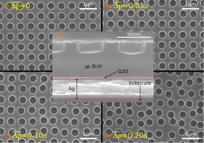
A substrate-type thin-film c-Si:H PV cell with light-trapping capability is typically fabricated by depositing the active layer on a textured back reflector such that the pattern is then transferred throughout the entire device Python09 ; Sai12 . This specific design however has two principal disadvantages: firstly, patterning of the metallic layer may enhance unwanted plasmonic losses Palanchoke12 and secondly, the c-Si:H layer must be grown on a non-uniform surface which due to the onset of more grain boundaries and defects during film growth act as recombination centers degrading its charge-transport properties Python09 . As a result, in this work we take a different approach and form the light-trapping structure directly within only the active layer itself. Our device, a precursor to a fully-functional PV cell, is fabricated on top of a base substrate using conventional thin-film deposition tools as follows. First, a back reflector consisting of a 270nm silver (Ag) film is placed on the substrate via electron-beam physical-vapor deposition. Next, a thin 40nm layer of gallium-doped zinc oxide (GZO) with carrier density and mobility of 5x1019cm-3 and 18cm2/(Vs) is sputtered on top followed by growth of the main active layer: 510nm of intrinsic c-Si:H via plasma-enhanced chemical vapor deposition (PECVD) with hydrogen (H2) and silane (SiH4) feed-in gases. The crystallinity fraction of the c-Si:H film is found using Raman spectroscopy to be 59% by fitting it to a combination of the known spectra of amorphous and crystalline silicon Vallat06 . Then, electron-beam lithography is used to define the two-dimensional PC pattern over an area of 2107x2107 periods of the square lattice (approximately 1.5mm2) in the spun-on positive resist which is followed by inductively-coupled plasma (ICP) reactive-ion etching (RIE) to create arrays of cylindrically-shaped holes on the top surface. Lastly, the resist residue is removed by soaking the samples in trichloroethylene followed by O2 plasma ashing. Note that while this device is sufficient for investigating the optical-absorption characteristics of the active c-Si:H layer, the focus of this work, it can be readily extended to a complete PV cell through an additional three processing steps: growing a -doped c-Si:H layer on top of a hole-etched intrinsic layer which sits above an -doped layer to form an n-i-p junction, sputtering another layer of transparent conductive oxide (e.g. ITO) with thickness of roughly 70nm on top of this c-Si:H layer and finally depositing a finger-grid of silver electrodes on the front surface. The electron-beam lithography and dry plasma etching used here to create a prototype design can be easily replaced by standard photo-lithography followed by a wet etch which is more practical for large-area fabrication Sai12 . Etching holes into the c-Si:H film is likely to introduce structural defects though confined to just the top surface; however if the holes can be made both sufficiently small and smooth while still retaining features of the Bloch modes the impact of such film-quality degradation may be mitigated while still providing many more degrees of design freedom in the choice of lattice for light trapping.
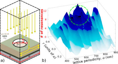
The thin-film PC structure which maximizes the light-trapping efficiency, a figure of merit we defined previously in Oskooi12 , can be obtained from a two-part design strategy Oskooi13 : 1) maximize the number of resonant-absorption modes and 2) apply a partial amount of disorder to boost broadband light trapping and robustness. While we have already shown that there exists a close correlation between the number of absorption resonances and the light-trapping efficiency Oskooi13 , it is worthwhile to reiterate that the design process is facilitated by the former due to both its direct connection to quasi resonances and better suitability as an objective function for topology optimization where a gradient-free search of a large parameter space is necessary. This is the case even though the latter which is proportional to the short-circuit current is a more-explicit measure of PV cell performance. For the first step, we use the open-source FDTD software tool Meep Oskooi10 to exhaustively explore the PC design space consisting of just two parameters in its unit cell as shown in the schematic of Fig. 1a: the lattice periodicity and hole radius (the hole height is fixed at 180nm; a somewhat arbitrary value that nonetheless gives rise to meaningful results). In order to ensure that the absorptivity spectra of our computational design agrees well with its experimental realization, we need to accurately incorporate the full complex-refractive index profile of c-Si:H over a broad bandwidth into the FDTD simulations. Here we focus on the wavelength interval spanning 700nm to 1000nm where the absorption coefficient of c-Si:H is small (less than approximately 1000cm-1 and decreasing Vallat06 ) and thus the need for a light-trapping design is most relevant. As it turns out, in this specific regime the complex-refractive index profile of c-Si:H is very similar to that of crystalline silicon (c-Si) Vetterl00 ; Vallat06 allowing us to make use of the extensively-compiled data of the latter Green08 . We therefore perform a nonlinear fit of the c-Si experimental data to a slightly-modified Drude-Lorentzian polarizability term used in the FDTD simulations Oskooi13 and obtain a close match in both the real part of the refractive index and the absorption coefficient. For even greater accuracy, we also incorporate into the simulations the material losses of GZO used in our actual device by first measuring its absorptivity in a separate experiment and then from this computing its absorption coefficient using a transfer-matrix approach Yeh88 . We will demonstrate later on that though GZO’s absorption coefficient may be large relative to that of c-Si:H (particularly at long wavelengths), nevertheless its absorption as a fraction of the total in the overall device is insignificant given that it is so much thinner and placed behind the c-Si:H layer. Figure 1b shows a contour plot of the number of absorption resonances - obtained from the simulated absorptivity spectra at normal incidence where the peak-identification threshold criteria is taken to be a constant 80% absorptivity at all wavelengths with no constraints on the peaks’ width or spacing relative to other peaks - as a function of the lattice periodicity and radius. The dotted green circle denotes the region where the number of peaks is largest and from which we select exemplary PC parameters for fabrication: =650nm and =208nm.
The fabricated PC device along with three of its partially-disordered variants where the position of the holes in the perfect lattice has been perturbed by an amount chosen randomly from a uniform distribution of values between 0 and for both orthogonal in-plane directions (=0.05, 0.10, 0.20) is shown in Fig. 2a-d. Some slight non-uniformity is evident in the hole shapes which will naturally tend to broaden the sharp absorption peaks found in the otherwise perfect case as will be apparent soon. A cross section of the entire device is shown in Fig. 2e where the three individual layers can be seen as well as the profile of the etched holes, with its somewhat uneven morphology which also contributes to the intrinsic imperfections affecting device performance. The presence of surface roughness on the c-Si:H film with feature sizes of less than 20nm does not significantly affect the absorption properties of the device unlike the irregularities associated with the holes which we confirmed separately with simulations; this is to be expected since the latter form the primary scattering objects of the lattice and thus more strongly influence the delicate-interference effects underlying the coherent nature of the guided resonant modes.
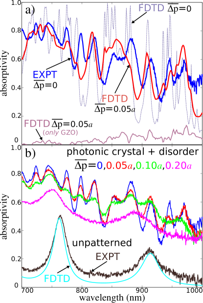
Next we measure the absorptivity spectra via 1-reflectivity of the unperturbed (=0) sample in an integrating sphere connected to a spectrometer and multi-channel Si detector using a tungsten halogen lamp source with a 610nm low-pass filter for -polarized light at an angle of incidence of 10∘. The results shown in Fig. 3a (in blue) display traces of numerous absorption resonances but all have noticeably undergone a minor degree of broadening due to the non-uniformities inherent in the holes’ morphology as discussed previously. This becomes evident when these experimental results are compared with those from two FDTD simulations (computed using identical incident-light conditions as the experimental measurements): one for =0 and the other for =0.05 where good agreement is apparent between the fabricated sample with =0 and simulated one with =0.05 (here three separate simulations are made using a 10x10 supercell and the absorptivity spectra is averaged due to the random nature of the design). This therefore suggests that from the perspective of light trapping the amount of intrinsic imperfections present within the fabricated sample is approximately equivalent to a positional disorder of =0.05 which is sufficiently minor so as to still confer an overall benefit to the device performance. Also shown in Fig. 3a is the absorptivity spectra of just the GZO layer for the =0.05 device (computed in FDTD again with three separate simulations by subtracting the absorptivity of the device with GZO absorption from one without which though not exact is still mostly accurate) demonstrating the relatively small absorption in this very thin 40nm layer that tends to increase somewhat with wavelength as the absorption coefficient of c-Si:H becomes smaller. The large discrepancy between the experimental and simulated results at wavelengths near 1000nm can be attributed to the weak sensitivity of the detector in this region which is visible in the low signal-to-noise ratio of the measured data. Figure 3b shows the measured absorptivity spectra of the four PC samples and demonstrates gradual broadening of the resonant-absorption peaks with increasing disorder and thus the onset of quasi resonances consistent with our prior observations Oskooi12 . Note however that the absorptivity spectra for the =0.20 device shows no traces of the resonant modes indicating that the amount of partial lattice disorder necessary to broaden the absorption peaks to the maximal extent without destroying them altogether - the key principle for creating quasi resonances with optimal light-trapping characteristics Oskooi12 - in the actual fabricated samples as a result of the intrinsic imperfections is markedly less than that of the ideal designs typically used in the simulations. The absorptivity spectra of the same device with an unpatterned c-Si:H layer is also shown for reference with its broad Fabry-Pérot resonances where in the absence of a light-trapping structure the absorptivity at each wavelength over the entire interval is considerably less than that of its partially-disordered PC counterparts. The corresponding data from an FDTD simulation is also shown for comparison to highlight both the presence and quantity of constant background absorption in the experiments due to the incomplete collection of light within the integrating sphere.
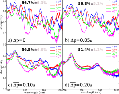
We continue to experimentally measure the angular dependence of the absorptivity spectra of the perfect and three partially-disordered thin-film PC devices in Fig. 4 at four angles of incidence - 10∘, 20∘, 30∘ and 40∘ - again for incident -polarized light. The performance of each device is quantified using its light-trapping efficiency averaged over the four angles as well as its standard deviation to gauge robustness. Though the efficiency is calculated using the broadband absorption of the entire device which includes that of the GZO layer, the results are still relevant for assessing the performance of a potential PV cell primarily because the GZO absorption is relatively small as was demonstrated earlier. Figure 4a shows just how sensitively the position of the resonant-absorption peaks of the unperturbed PC structure depend on the incident conditions and the degree to which this can be made less and less so with the gradual addition of disorder just as we had previously observed with simulations Oskooi12 . The light-trapping efficiency increases with partial lattice disorder (attaining a maximum of 56.8% at =0.05 in Fig. 4b) before decreasing considerably to 51.4% at =0.20 again generally consistent with our earlier findings Oskooi12 . The dual integration of lattice disorder and fabrication imperfections is perhaps best represented by the nearly-optimal partially-disordered PC device with =0.10 (in Fig. 4c) which is nearly 10% above in efficiency and more than twice as robust as the ideal design (47.9% 8.2%) as computed by simulations.
In summary, we have experimentally shown how quasi resonances can be incorporated into a thin-film silicon device as a PC with a controlled amount of partial lattice disorder augmented with unintentional fabrication-induced imperfections to boost light trapping over a broad bandwidth and angular range. The design process was enabled by accurate FDTD simulations to both structure the active-layer PC and to more fully investigate absorption in the rest of the device. A further extension of this design strategy to a complete thin-film micro-crystalline PV cell possibly based on the guidelines we have outlined is the next step for investigating the role of quasi resonances on increasing overall efficiency.
This work was supported by Core Research for Evolutional Science and Technology (CREST) from the Japan Science and Technology agency. A.O. was supported by a postdoctoral fellowship from the Japan Society for the Promotion of Science (JSPS). We also thank Yosuke Kawamoto and Pedro Favuzzi of Kyoto University for fruitful discussions.
References
- (1) J. Poortmans and V. Arkhipov, Thin Film Solar Cells: Fabrication, Characterization and Applications (John Wiley & Sons, Ltd, 2006).
- (2) S. Pillai, K. Catchpole, T. Trupke, and M. Green, “Surface plasmon enhanced silicon solar cells,” J. Appl. Phys. 101 (2007).
- (3) E. Garnett and P. Yang, “Light trapping in silicon nanowire solar cells,” Nano Lett. 10, 1082–1087 (2010).
- (4) S. Han and G. Chen, “Toward the lambertian limit of light trapping in thin nanostructured silicon solar cells,” Nano Lett. 10, 4692–4696 (2010).
- (5) X. Sheng, J. Liu, I. Kozinsky, A. Agrawal, J. Michel, and L. Kimerling, “Design and non-lithographic fabrication of light trapping structures for thin film silicon solar cells,” Adv. Mater. 23, 843–847 (2011).
- (6) C.-M. Hsu, C. Battaglia, C. Pahud, Z. Ruan, F.-J. Haug, S. Fan, C. Ballif, and Y. Cui, “High-efficiency amorphous silicon solar cell on a periodic nanocone back reflector,” Adv. Ene. Mater. 2, 628–633 (2012).
- (7) H. Sai, K. Saito, and M. Kondo, “Enhanced photocurrent and conversion efficiency in thin-film microcrystalline silicon solar cells using periodically textured back reflectors with hexagonal dimple arrays,” Appl. Phys. Lett. (2012).
- (8) A. Oskooi, P. Favuzzi, Y. Tanaka, H. Shigeta, Y. Kawakami, and S. Noda, “Partially-disordered photonic-crystal thin films for enhanced and robust photovoltaics,” Appl. Phys. Lett. 100 (2012).
- (9) A. Oskooi, Y. Tanaka, and S. Noda, “Tandem photonic-crystal thin films surpassing lambertian light-trapping limit over broad bandwidth and angular range,” arxiv: 1304.5329 (2013).
- (10) A. F. Oskooi, D. Roundy, M. Ibanescu, P. Bermel, J. D. Joannopoulos, and S. G. Johnson, “MEEP: A flexible free-software package for electromagnetic simulations by the FDTD method,” Computer Physics Communications 181, 687–702 (2010).
- (11) M. Python, O. Madani, D. Domine, F. Meillaud, E. Vallat-Sauvain, and C. Ballif, “Influence of the substrate geometrical parameters on microcrystalline silicon growth for thin-film solar cells,” Sol. Ener. Mat. and Sol. Cells 93, 1714–1720 (2009).
- (12) U. Palanchoke, V. Jovanov, H. Kurz, P. Obermeyer, H. Stiebig, and D. Knipp, “Plasmonic effects in amorphous silicon thin film solar cells with metal back contacts,” Opt. Express 20, 6340–6347 (2012).
- (13) E. Vallat-Sauvain, A. Shah, and J. Bailat, Advances in Microcrystalline Silicon Solar Cell Technologies (John Wiley & Sons, Ltd., 2006), chap. 4.
- (14) O. Vetterl, F. Finger, R. Carius, P. Hapke, L. Houben, O. Kluth, A. Lambertz, A. Muck, B. Rech, and H. Wagner, “Intrinsic microcrystalline silicon: A new material for photovoltaics,” Sol. Ener. Mat. & Sol. Cells 62, 97–108 (2000).
- (15) M. Green, “Self-consistent optical parameters of intrinsic silicon at 300 k including temperature coefficients,” Solar Energy Materials and Solar Cells 92, 1305–1310 (2008).
- (16) P. Yeh, Optical Waves in Layered Media (Wiley, New York, 1988).