Transmission electron microscopy and ferromagnetic resonance investigations of tunnel magnetic junctions using Co2MnGe Heusler alloy as magnetic electrodes
Abstract
High resolution transmission electronic microscopy, nano-beam electronic diffraction, energy dispersive X-rays scanning spectroscopy, Vibrating Sample Magnetometry (VSM) and FerroMagnetic Resonance (FMR) techniques are used in view of comparing (static and dynamic) magnetic and structural properties of Co2MnGe (13 nm)/Al2O3 (3 nm)/Co (13 nm) tunnel magnetic junctions (TMJ), deposited on various single crystalline substrates (a-plane sapphire, MgO(100) and Si(111)). They allow for providing a correlation between these magnetic properties and the fine structure investigated at atomic scale. The Al2O3 tunnel barrier is always amorphous and contains a large concentration of Co atoms, which, however, is significantly reduced when using a sapphire substrate. The Co layer is polycrystalline and shows larger grains for films grown on a sapphire substrate. The VSM investigation reveals in-plane anisotropy only for samples grown on a sapphire substrate. The FMR spectra of the TMJs are compared to the obtained ones with a single Co and Co2MnGe films of identical thickness deposited on a sapphire substrate. As expected, two distinct modes are detected in the TMJs while only one mode is observed in each single film. For the TMJ grown on a sapphire substrate the FMR behavior does not significantly differ from the superposition of the individual spectra of the single films, allowing for concluding that the exchange coupling between the two magnetic layers is too small to give rise to observable shifts. For TMJs grown on a Si or on a MgO substrate the resonance spectra reveal one mode which is nearly identical to the obtained one in the single Co film, while the other observed resonance shows a considerably smaller intensity and cannot be described using the magnetic parameters appropriate to the single Co2MnGe film. The large Co concentration in the Al2O3 interlayer prevents for a simple interpretation of the observed spectra when using Si or MgO substrates.
I Introduction
Spin electronics is an emerging technology exploiting the spin of electron as an information carrier. Tunnel magnetic junctions (TMJ), consisting of a tunnelling barrier sandwiched between two ferromagnetic electrodes, belong to devices presenting a great interest due to their use in magnetic memories [1], in low field magnetic sensors [2] and in microwave components for spintronic applications [3] for which high tunnel magnetoresistance ratios (TMR) are highly desirable. TMR is directly related to the spin polarization of ferromagnetic electrodes [4]. Therefore, half metallic materials such as Heusler alloys, such as NiMnSb, PtMnSb and Co-based Heusler compounds like Co2MnSi and Co2MnGe, should be ideal compounds as high spin polarized current sources allowing for realizing large TMR values. The efficiency of a TMJ, and therefore its TMR value, strongly depend on interfacial roughness, on inter-diffusion and on oxygen content, which in turn depend on the materials used in the stack and on the conditions of deposition and of annealing. Furthermore, the substrate material as well as its orientation have an impact on the magnetic anisotropy of the magnetic thin films, and thus on the TMR value, because of the band hybridization and of the spin-orbit interaction at the interface. Therefore, the control of such parameters should allow for enhancing the half-metallicity of the electrodes and thus for increasing the TMR values. Co-based Heusler alloys [5, 6] are promising materials for spintronic applications, because a number of them possess a high Curie temperature [6] and, therefore, may consist in alternative compounds to obtain half metallicity even at room temperature. These materials have been used as electrodes [7-10] in TMJs where TMR up to 360 has been demonstrated at room temperature [9, 10]. However, up to now, the demonstrated TMR amplitudes using Heusler alloys as magnetic electrodes in TMJs remain lower than the extremely large TMR at room temperature which has been predicted and demonstrated in TMJs using (001)-textured MgO as a tunnel barrier and normal transition metals or their alloys as electrodes [11, 12]. Apart from high TMR values, it is also important to understand the magnetization dynamics and the magnetic anisotropy of TMJs in relation with the interfacial characteristics for realizing high speed spintronic devices. Therefore, ferromagnetic resonance (FMR), vibrating sample magnetometer (VSM), ultrahigh resolution and scanning transmission electronic microscopy (HRTEM and STEM), nano-beam electronic diffraction and energy dispersive X-rays scanning spectroscopy (STEM-EDX) have been used for the investigation of static and dynamic magnetic properties in correlation with the atomic scale characterization of interfaces involved in Co2MnGe (13 nm)/Al2O3 (3 nm)/Co (13 nm) TMJs deposited on a-plane sapphire, on MgO and on Si substrates. The properties of a Co2MnGe/Al2O3/Co TMR device have been previously discussed by Verduijn et al. [13] and compared to those of a Co2MnGe/Al2O3/Co TMR element prepared using identical process parameters. They found a 27 TMR value at 77 K for Co2MnGe/Al2O3/Co, slightly larger than for a Co2MnGe/Al2O3/Co junction. However, at room temperature, the TMR value of Co2MnGe/Al2O3/Co drastically decreases to 9%. Therefore, in order to understand the reasons of this low TMR value at room temperature, magnetic properties are studied in this paper in close relation with the microstructural properties of Co2MnGe/Al2O3/Co TMJ.
II Samples preparation and experimental methods
The Co2MnGe(13nm)/Al2O3(3nm)/Co(13nm) TMJs were prepared in-situ under ultrahigh vacuum (UHV) conditions (base pressure Pa) using a combination of ion beam sputter deposition (IBSD) and UHV-magnetron sputtering on sapphire a-plane, Si(111) and MgO(100) substrates. The Co2MnGe layer was grown at a substrate temperature of C on a 4 nm thick Vanadium seed layer by UHV magnetron sputtering at a rate of 0.015 nm/s. After the deposition of the Heusler layer, the substrate was cooled down to room temperature, transferred to the IBSD chamber and then cleaned by ion beam etching with a 150 eV Ar-ion beam to remove any surface layer, which might have been oxidized during cooling down of the substrate. The Al2O3-layer is created by depositing 1.5 nm Al at room temperature at a sputtering rate of 0.08 nm/s and a subsequent RF plasma oxidation process in a separate oxidation chamber. The oxidation chamber was filled with pure oxygen gas at a pressure of 6 kPa, and the Al-layer was oxidized due to the applied RF-power of 5 W during 30 s. In a final step the Co-layer was deposited by IBSD with the substrate at room temperature at a sputtering rate of 0.03 nm/s and capped by a 4 nm Au protective layer. More details about the fabrication procedure can be found in [13].
The Co and Co2MnGe single layers, which serve as reference samples below, were prepared using the same procedures and keeping all parameters identical to those used during the preparation of the TMJs.
The characterization of the microstructures and elemental compositions of the TMJ grown on a-plane sapphire, MgO(100) and Si(111) substrates, were performed using a transmission electron microscope. Three TEM cross sections are prepared by in situ lift out using a Zeiss scanning electron microscope equipped with a Focused Ion Beam. To avoid damage from the high-energy ion beam during sample preparation, a platinum (Pt) layer was deposited to protect the sample surface. High resolution transmission electron microscopy and scanning transmission electron microscopy observations were carried out on a JEOL JEM ARM 200F (JEOL Ltd.) operating at 200 kV. This microscope was equipped with a field emission gun and an aberration (Cs) corrector on the electron probe. High angle annular dark field STEM (HAADF-STEM) images were acquired with a camera length of 8 cm and a probe size of 0.1 nm. The contrast of these micrographs is linked to the atomic number Z of the phase and thus permits to obtain a chemical contrast. Elemental compositions, with a precision of more or less 2 atom per cent (at.), were performed by STEM-EDX using a JEOL detector with a probe size of 0.4 nm.
Their magnetic dynamic properties have been studied by micro-strip ferromagnetic resonance (MS-FMR). The MS-FMR characterization was done with the help of a field modulated FMR setup using a vector network analyser (VNA) operating in the 0.1-40 GHz frequency range. The sample (with the film side in direct contact) is mounted on a 0.5 mm micro-strip line connected to the VNA and to a lock-in amplifier to derive the field-modulated measurements via a Schottky detector. This setup is piloted via a Labview program providing flexibility of a real time control of the magnetic field sweep direction, step and rate, real time data acquisition and visualization. It allows both frequency and field-sweeps measurements with magnetic fields up to 2 T applied parallel or perpendicular to the sample plane. In-plane angular dependence of resonance frequencies and fields are used to measure anisotropies. The complete analysis of in-plane and perpendicular field resonance spectra exhibiting the excited modes leads to the determination of most of the magnetic parameters: effective magnetization, gyromagnetic factor, interlayer exchange coupling and anisotropy terms.
III HRTEM and STEM characterization
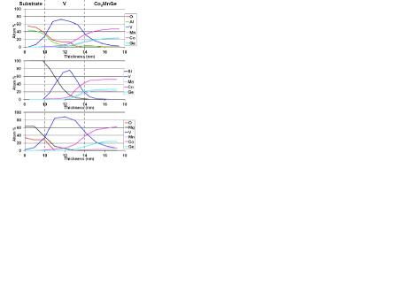
Figure1 shows the TMJ structure for the three samples. These structures consist in a stack of layers with different elemental compositions. On the STEM-HAADF micrograph, larger is the average atomic number of the layer, brighter it appears. The three samples present a similar structure with the succession of the following layers: substrate/V/Co2MnGe/Al2O3/Co/Au. The interfaces seem to be well defined and flat, except for the Co/Au one, which is very rough and wavy. The Au layer is not uniform and presents some holes. The average thicknesses of the V, Al2O3 and Co layers do not depend on the different substrates and are respectively: 4 nm, 3-4 nm and 8-11 nm. An example of thickness measurement is presented on figure 1d. The variation of the Co layer thickness reflects the roughness of its interface with the gold layer. Concerning the thickness of the Co2MnGe layer, it depends on the substrate: it is of about 13 nm for the sapphire and Si substrates but of only 10 nm for the MgO substrate. The thickness measurements have been carried out on the STEM micrographs with a precision of 1 nm.
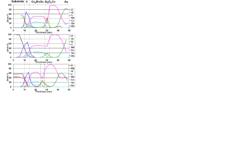
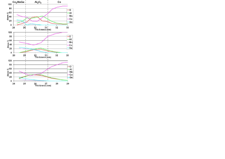
The dependence of the elemental composition versus the coordinate normal to the sample was obtained for the three TMJs using EDX line scans. The results are shown on figure 2. In each layer, mainly due to inter-diffusion, the elemental concentration differs from the expected nominal one and is not uniform. The detailed mapping of the elemental composition depends on the substrate. Notice that the thin film of Al2O3 separating the two magnetic layers contains a very high concentration of Co in the case of MgO or of Si substrates (average value overpassing 40 at.) and a rather smaller one (average value overpassing 20 at.) for a sapphire substrate. The effective structure is poorly approximated by an abrupt Co2MnGe/Al2O3/Co trilayers arrangement, except, maybe, in the case of a sapphire substrate. In addition, with the MgO substrate, the Mn concentration in the Heusler film lies well below the expected value (7 at. instead of 25 at.). More generally, accurate EDX line scans (see Figures 3 and 4) show that around every interface there is an important inter-diffusion of the constitutive elements of adjacent layers: as a result the elemental composition of each layer is strongly modified near its interfaces on a distance of about 2 nm. Due to the small thickness (3 nm) of the Al2O3 film some alteration of the properties of the studied TMJs is expected.
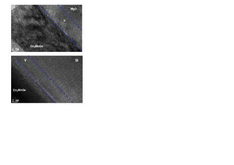
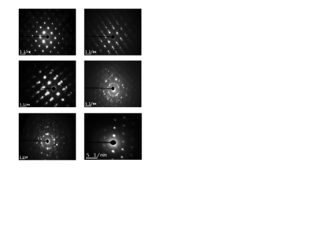
HRTEM micrographs and nano-beam diffractions have permitted to check the crystalline quality of the different layers and the epitaxial relationships. The substrate and the vanadium layer are monocrystalline and the vanadium layer shows a perfect epitaxy with the substrate. This is illustrated, in the case of the MgO substrate, by a micrograph in figure 5a and by two diffraction patterns in Figures 6a and 6b related to MgO and to the vanadium layer, respectively: the ()V plane of the vanadium layer coincides with the ()MgO plane of the substrate, as expected. The diffraction patterns shown in Figure 6c and in Figure 6d concern the Co2MnGe layer, near of the V/Co2MnGe interface and in the vicinity of its centre, respectively: the rather good epitaxy observed near the interface does not persist in the central region which shows a polycrystalline distribution, as attested by the presence of different diffraction spots arising from many different nano-grains. For the three studied TMJs, the Al2O3 barrier is amorphous and the Co layer is found to be polycrystalline, as resulting from multiple diffraction spots arising from its central region (Figure 6e). However, for the TMJ grown on a sapphire substrate, the mean size of the nano-grains is substantially increased, allowing for observing nano-beams diffraction patterns related to only one grain, as shown in Figure 6f.
In conclusion, the studied TMJs show an important inter-diffusion between their constitutive layers, and present polycrystalline magnetic films. However, the use of a sapphire substrate seems to provide the best choice in view of obtaining TMJs of good quality (smallest diffusion and largest nano-grains).
IV Magnetic properties
The experimental magnetic dynamic data have been analysed considering a magnetic energy density characterized by Zeeman, demagnetizing and anisotropy contributions given by equations (1) and (2) respectively for Co2MnGe and Co respectively:
(1)
(2)
In the above expressions, is the applied magnetic field; the other parameters stand for the saturation magnetization (), for the perpendicular anisotropy contribution (), for the two-fold (, ) and the four-fold in-plane anisotropy contributions (), using the additional suffixes labeling the concerned layer ( for Co2MnGe or for Co). The out-of-plane () and in-plane directions () also appear with the appropriate indices. Tentatively, the total magnetic energy of the TMJ consisting in two magnetic layers of thicknesses and can be written as:
(3)
Above, defines a bilinear exchange coupling between the two films.
In an applied magnetic field two uniform magnetic modes result from the above expression of the energy: their frequencies are obtained in the usual way by solving the equations of motion of the magnetizations [14] around their equilibrium positions (these positions are obtained by minimizing ). Indeed, in the absence of coupling (), the two frequencies do not differ from their values in each single layer (which are proportional to the gyromagnetic factor and , for and , respectively). Conversely, at a fixed frequency one expects for two different resonant in-plane magnetic fields applied in any defined direction. In the following, as usual, we introduce, with the appropriate suffixes or , the effective Landé factors GHz/T, where is the absolute value of the electron charge and is its mass), the effective demagnetizing fields (), the uniaxial in-plane anisotropy field and the fourfold in-plane anisotropy field .
IV.1 Static magnetic measurements
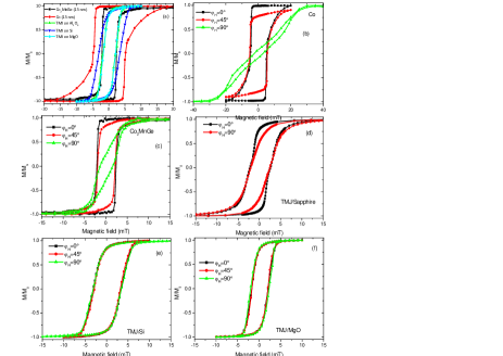
The coercive fields are strongly dependent function of the anisotropy fields, of the magnetostatic interaction and of the exchange interaction between the magnetic films. All these quantities depend on the chemical composition, on the morphology and on the crystalline structure of the thin films. For all the studied samples the hysteresis loops were obtained by VSM with an in-plane magnetic field applied along various orientations (where is the in-plane angle between the magnetic applied field and one of the edges of the substrate). Figure 7 shows representative behaviors of these samples. The observed shape mainly depends on the field orientation both for single layers and TMJ grown on sapphire, in agreement with the presence of in-plane anisotropy. In contrast, the hysteresis loops of TMJs grown on Si and MgO do not depend on , suggesting the absence of anisotropy (Fig. 7e and 7f). The magnetization loops along the easy axis are shown on figure 7a for the two single layers and for the three TMJs. The values lie near 2.3 mT, except for the Co single layer, which presents a higher (4.8 mT). Figure 7b illustrates the high in-plane anisotropy observed in the Co single layer: along the hard axis the saturation field for magnetization is 30 mT). The presence of Co magnetic anisotropy in TMJ on sapphire substrate and its disappearance in TMJs on Si and MgO substrates suggest that this uniaxial anisotropy is most probably induced by the interface with the sapphire substrate [15]. As confirmed below by FMR, the hysteresis loops of the Co2MnGe single layer (Fig. 7c) reveal that its planar anisotropy consists of the superposition of a fourfold contribution, with easy axes parallel to the substrate edges, and of a uniaxial term. The fourfold anisotropy is presumably of magnetocrystalline nature while we attribute the uniaxial contribution at least partially originating from a slight misorientation of the surface of the substrate as discussed in details in [16, 17]. Finally, the hysteresis loop of the TMJ grown on sapphire presents a narrow plateau at small applied fields, suggesting that Co and Co2MnGe layers (Fig. 7d) are uncoupled, and that their coercive fields are very close from each other, which implies a significant decrease of the Co anisotropy, compared to the single Co layer. However, for TMJs on Si and on MgO, the absence of anisotropy for the two magnetic layers explains the complete disappearance of any double switching behaviour. The presence of anisotropy in TMJ grown on sapphire is presumably related to their best quality, as shown by the above microstructural characterization.
In addition, variations of the reduced remanent magnetization (), as function of , of the single layers are also shown in view of comparison with other results discussed in the next section.
IV.2 Dynamic measurements
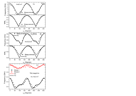
In a first step the magnetic parameters of the individual layers were derived with the help of the FMR study of our single magnetic Co and Co2MnGe films. In these films, only one resonance mode is observed, as expected. Figures 8a and 8b illustrate the experimental in-plane angular dependence of the frequency of the uniform mode for Co and Co2MnGe layers respectively, compared to our best fits using the model above described. The derived values of the magnetic parameters corresponding to these best fits are reported in Table I. Notice that a uniaxial term well describes the in-plane anisotropy in the Co sample while both uniaxial and fourfold in-plane anisotropy terms are requested to give account for the data concerning Co2MnGe. In addition, the derived in-plane anisotropy characteristics are consistent with the above mentioned angular variation of the reduced remanent magnetization ().
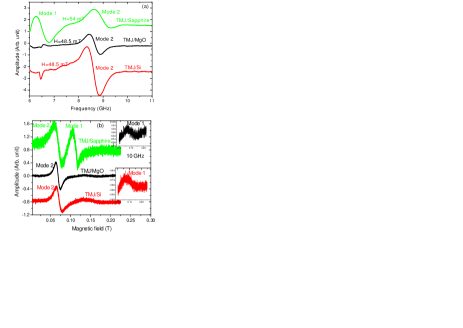
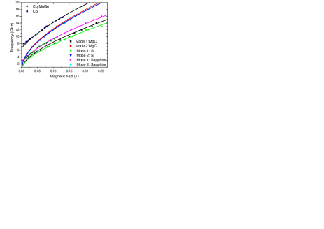
In the TMJs, two resonance modes should be present in the FMR spectra. For sweep frequency measurements using an in-plane applied magnetic field, such a twofold behavior is only observed for the TMJ grown on sapphire (Fig. 9a) while the TMJs grown on MgO or on Si show a unique resonance line. The indices 1 and 2 are used to refer to the lower and to the higher frequency mode present with a sapphire substrate, respectively. In the case of a MgO or of a Si substrate the resonance frequency lies near of the value observed for the mode 2 in the TMJ deposited on sapphire. Sweep field measurements (Fig. 9b) allow for the detection of the two modes whatever is the substrate, maybe due to the best sensitivity. However, compared to the case of sapphire, the intensity of mode 1 is significantly reduced with MgO or Si substrates. Let us remember that it results from the STEM investigation that with Si or MgO, the Al2O3 interlayer contains a high concentration of inter-diffused Co: the description of the studied structure in terms of a junction between two well separated homogeneous magnetic layers then becomes rather poor. On the other hand, it is probable that the best quality of Co2MnGe layers is obtained using a sapphire substrate.
The field dependences of the frequencies of the observed modes for the three TMJs, compared to those of the single layers, are shown on Figure 10. Assuming that the exchange coupling does not induce very strong perturbations among the two modes, one of them represents a Co-like uniform magnetic excitation and the other one represents a Heusler-like uniform magnetic excitation. Due to the field dependence of mode 2 it is assigned to consist in the Co-like uniform mode: a preliminary derivation neglecting any coupling leads an effective -factor of 2.17 and to a demagnetizing field ranging in the (1.47-1.54) T interval, to compare the 2.17 and 1.55 T values respectively found for the single Co layer. Indeed, mode 1 is identified as the Heusler-like one: for the TMJ grown on a sapphire substrate, the same approximation leads to and to a demagnetizing field of 0.95 T, identical to the values found for the single Heusler layer. However, in the case of MgO or of Si substrates the demagnetizing field is substantially reduced: the highly Co concentrated interlayer seems to induce a perpendicular anisotropy but the interpretation of the result is missing. Concerning the in-plane anisotropy, it was derived for mode 2 in the three available TMJs through the in-plane angular dependence of the FMR spectra: in the case of an MgO or of a Si substrate it vanishes; with a sapphire substrate (Figure 8c) it consists into a rather small uniaxial contribution ( = 1.1 mT). Notice that the single Co layer is affected by a high uniaxial contribution (30 mT, see Figure 8a): this put in evidence the difference between the (crystalline sapphire)-Co and the (amorphous alumina)-Co interfacial interaction. The in-plane anisotropy relative to mode 1 could be only studied in the TMJ grown on a sapphire substrate (Fig. 8b): it can be described as deriving from the superposition of a four-fold symmetry term and of a uniaxial one, a behaviour analogous to the observed one in the single Heusler layer (Figure 8b).
Finally, it appears that the fit of our data cannot be improved by taking in account the exchange interaction: a large exchange would induce similar shifts for mode 1 and mode 2, in contrast with the observed results. In view of the other variations of the parameters monitoring the resonance the exchange is too small to be derived from the FMR studies. However, this small exchange can be detected from the analysis of the static magnetic properties.
V Conclusion
Co2MnGe(13nm)/Al2O3(3 nm)/Co(13nm) TMJs deposited on a-plane sapphire, MgO and Si substrates have been prepared. For comparison, single films of Co2MnGe and of Co with a thickness of 13 nm have been also deposited on sapphire. Their nanoscale structure, compared to their static and dynamic magnetic properties, have been studied. The ultrahigh resolution transmission electron microscopy revealed differences between the TMJs which have a direct impact on their magnetic characteristics. The FMR measurements show the presence of two modes deriving from the Co and from the Co2MnGe layer which are only very weakly coupled. The magnetic parameters of these modes depend on the quality of the TMJ and more or less differ from those of the single layers.
References
- (1) R. W. Dave, G. Steiner, J. M. Slaughter, J. J. Sun, B. Craigo, S. Pietambaram, K. Smith, G. Grynkewich, M. DeHerrera, J. Åkerman, and S. Tehrani, IEEE Trans. on Magn. 42, 1935 (2006)
- (2) P. P. Freitas, R. Ferreira, S. Cardoso and F. Cardoso, J. Phys.: Condens. Matt. 19, 165221 (2007)
- (3) A. A. Tulapurkar, Y. Suzuki, A. Fukushima, H. Kubota1, H. Maehara, K. Tsunekawa, D. D. Djayaprawira, N. Watanabe and S. Yuasa, Nature 438, 339 (2005)
- (4) M. Julliere, Phys. Lett. 54A, 225 (1975).
- (5) K. Inomata, N. Ikeda, N. Tezuka, R. Goto, S. Sugimoto, M. Wojcik and E. Jedryka, Sci. Technol. Adv. Mater. 9, 014101 (2008)
- (6) S. Trudel, O. Gaier, J. Hamrle, and B. Hillebrands, J. Phys. D: Appl. Phys. 43, 193001 (2010)
- (7) M Yamamoto, T Marukame, T Ishikawa, K Matsuda, T Uemura and M Arita, J. Phys. D: Appl. Phys. 39, 824 (2006)
- (8) K. Inomata, N. Ikeda, N. Tezuka, R. Goto, S. Sugimoto, M. Wojcik and E. Jedryka, Sci. Technol. Adv. Mater. 9, 014101 (2008)
- (9) W. H. Wang, E. Liu, M. Kodzuka, H. Sukegawa, M. Wojcik, E. Jedryka, G. H. Wu, K. Inomata, S. Mitani, and K. Hono, Phys. Rev. B 81, 140402 (R) (2010)
- (10) W. H. Wang, H. Sukegawa, and K. Inomata, Phys. Rev. B 82, 092402 (2010)
- (11) S. Ikeda, J. Hayakawa, Y. Ashizawa, Y. M. Lee, K. Miura, H. Hasegawa, M. Tsunoda, F. Matsukura, and H. Ohno, Appl. Phys. Lett. 93, 0852508 (2008)
- (12) L. Jiang, H. Nagauma, M. Oogane, and Y. Ando, Appl. Phys. Express 2, 083002 (2009)
- (13) E. A. Verduijn and K. Westerholt, J. Appl. Phys. 99, 084502 (2006)
- (14) S. M. Rezende, C. Chesman, M. A. Lucena, A. Azevedo, F. M. de Aguiar, and S. S. P. Parkin, J. Appl. Phys. 84, 958 (1998)
- (15) N. Metoki, Th. Zeidler, A. Stierle, K. Bröhl and H. Zabel, J. Magn. Magn. Mater. 118, 57 (1992)
- (16) M. Belmeguenai, F. Zighem, Y. Roussigné, S.-M. Chérif, P. Moch, K.Westerholt, G.Woltersdorf, and G. Bayreuther, Phys. Rev. B 79, 024419 (2009)
- (17) M. Belmeguenai, F. Zighem, T. Chauveau, D. Faurie, Y. Roussigné, S.-M. Chérif, P.Moch, K.Westerholt, and P.Monod, J. Appl. Phys.108, 063926 (2010)