Valley filter from magneto-tunneling between single and bi-layer graphene
Abstract
We consider tunneling transport between two parallel graphene sheets where one is a single-layer sample and the other one a bi-layer. In the presence of an in-plane magnetic field, the interplay between combined energy and momentum conservation in a tunneling event and the distinctive chiral nature of charge carriers in the two systems turns out to favor tunneling of electrons from one of the two valleys in the graphene Brillouin zone. Adjusting the field strength enables manipulation of the valley polarization of the current, which reaches its maximum value of 100% concomitantly with a maximum of the tunneling conductance.
pacs:
73.22.Pr 72.80.Vp 85.75.MmThe concept of spintronics Žutić, Fabian, and Das Sarma (2004) continues to stimulate the detailed study of intertwined dynamics of intrinsic (pseudo-)spin-1/2 degrees of freedom and the orbital motion of charge carriers Sinova and Žutić (2012). Graphene-based nanomaterials Weiss et al. (2012) are particularly attractive systems for spintronics applications Pesin and MacDonald (2012) because, in addition to their ordinary spin, electrons in graphene also carry an orbital pseudo-spin and a valley-isospin degree of freedom Castro Neto et al. (2009). While the pseudo-spin-up/down eigenstates correspond to an electron’s position on the two equivalent sublattices of graphene’s honeycomb lattice in real space, the valley-isospin quantum number distinguishes states near the and high-symmetry points in reciprocal space. Schematics of the single-layer and bi-layer graphene lattices as well as their (identical) Brillouin zone(s) are shown in panels (a)–(c) of Fig. 1.
The possibility to realize valley-isospin-based spintronics , called valleytronics, in graphene has attracted a lot of interest Xiao, Yao, and Niu (2007); Rycerz, Tworzydło, and Beenakker (2007); Yao, Xiao, and Niu (2008); Garcia-Pomar, Cortijo, and Nieto-Vesperinas (2008); Abergel and Chakraborty (2009); Fujita, Jalil, and Tan (2010); Low and Guinea (2010); Zhai et al. (2010); Schomerus (2010); Wu et al. (2011); Gunlycke and White (2011); Golub et al. (2011); Jiang et al. (2013); Wu, Lue, and Chen (2013); Khatibi, Rostami, and Asgari (2013). The operation of valleytronic devices generally depends on the ability to generate valley-asymmetric charge currents. Mechanisms to separately address electrons from individual valleys necessarily involve the breaking of inversion and/or time-reversal symmetries Xiao, Yao, and Niu (2007), e.g., via nanostructuring Rycerz, Tworzydło, and Beenakker (2007); Schomerus (2010), coupling to electromagnetic fields Yao, Xiao, and Niu (2008); Garcia-Pomar, Cortijo, and Nieto-Vesperinas (2008); Abergel and Chakraborty (2009); Fujita, Jalil, and Tan (2010); Low and Guinea (2010); Zhai et al. (2010); Golub et al. (2011); Wu, Lue, and Chen (2013); Khatibi, Rostami, and Asgari (2013), application of mechanical strain Fujita, Jalil, and Tan (2010); Low and Guinea (2010); Zhai et al. (2010); Wu et al. (2011); Jiang et al. (2013); Khatibi, Rostami, and Asgari (2013), or presence of defects Gunlycke and White (2011). In many of these situations, the mobility of charge carriers could be compromised by the required inhomogeneity and/or orbital effects of the applied external fields.
Here we propose a valley-filter device that is based on resonant electron tunneling between parallel single-layer and bi-layer graphene sheets. Vertical heterostructures of two-dimensional (2D) crystals have recently been fabricated Britnell et al. (2012a, b); Georgiou et al. (2012); Britnell et al. (2013); Geim and Grigorieva (2013); Myoung et al. (2013), and their electronic properties have become the subject of detailed theoretical study Feenstra, Jena, and Gu (2012); Bala Kumar, Seol, and Guo (2012); Vasko (2013); Pratley and Zülicke (2013). As discussed below, application of a magnetic field parallel to the graphene sheets enables direct tuning of the valley polarization of the tunneling current, with a possible maximum value of 100%. In contrast to other valley-filter designs, no significant modification of the graphene sheets’ electronic structure is required to enable valley-asymmetric transport. As an additional feature, a valley-polarized current is generated simultaneously in both the single-layer and the bi-layer sheets.
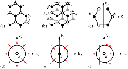
Our proposed valley-filter design utilizes the strong link between linear orbital momentum, pseudo-spin and valley isospin for electrons in graphene materials. Due to peculiarities of the honeycomb-lattice band structure, an electron’s pseudo-spin state is locked to its linear motion on the 2D graphene sheet in a way that is normally exhibited by ultra-relativistic (massless) Dirac fermions Castro Neto et al. (2009). The exact form of this coupling turns out to be different for electrons from the two valleys and also depends on the type of graphene structure, e.g., whether it is a single-layer or a bi-layer sample. See Fig. 1, panels (d)–(f), for an illustration. Furthermore, states with the same wave-vector shift from the high-symmetry point in the conduction and valence bands have opposite pseudo-spin polarization. The characteristic differences between valley-dependent pseudo-spin-momentum locking in single-layer and bi-layer graphene makes it possible to achieve valley separation in a momentum-resolved tunneling structure proposed here.
Tunneling transport between parallel 2D conductors exhibits strongly resonant behavior Smoliner et al. (1989); Eisenstein et al. (1991); Hayden et al. (1991); Gennser et al. (1991); Simmons et al. (1993) as a function of in-plane magnetic field and bias voltage because of the requirement to simultaneously conserve the canonical in-plane momentum and total energy of every tunneled electron. Theoretical descriptions of 2D-to-2D tunneling Zheng and MacDonald (1993); Lyo and Simmons (1993); Raichev and Vasko (1996); Jungwirth and MacDonald (1996) have been able to explain the experimental observations with great accuracy.
Recent progress in fabricating tunnel-coupled unconventional 2D systems where the charge carriers’ intrinsic (pseudo-)spin-1/2 degree of freedom is rigidly locked to their orbital motion has stimulated further interest Pershoguba and Yakovenko (2012); Vasko (2013); Pratley and Zülicke (2013). In particular, it has been shown Pratley and Zülicke (2013) that the linear (i.e., small-bias) magneto-tunneling conductance for electrons from valley ( or in graphene, or in an ordinary 2D quantum-well system) is given by
| (1) | |||||
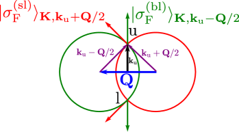
Here is the magnetic-field-induced shift in kinetic momentum Smoliner et al. (1989); Eisenstein et al. (1991); Hayden et al. (1991); Gennser et al. (1991); Simmons et al. (1993); Zheng and MacDonald (1993); Lyo and Simmons (1993); Raichev and Vasko (1996) for an electron that has tunneled between two layers spaced vertically at distance . The factor accounts for the real-spin degeneracy, is the density of states at the Fermi energy in system not including real-spin or valley degrees of freedom, is the Fermi wave vector in system , and
| (2) |
are overlap matrix elements between (pseudo-)spinors associated with the electron states at the two intersection points (labelled u and l, respectively) of the shifted Fermi circles. See Fig. 2 for an illustration.
In the following, we neglect the dependence of the tunneling matrix 111This is based on the realistic assumption that the tunnel-barrier height is much larger than the bandwidth of relevant electronic excitations. In principle, the -dependence of can modify the density dependence of tunneling conductances but will not affect the functionality of our proposed valley-filter device. and use the parameterization
| (3) |
with complex numbers that encode all possible tunneling processes, including those that are associated with a (pseudo-)spin flip. To be specific, we limit ourselves to the case where both the layers are n-doped, i.e., where . Because of the rigid locking between the pseudo-spin state and the kinetic momentum of single-electron eigenstates in single-layer and bi-layer graphene [see Figs. 1(d)–(f)], it is possible to express the spinors for positive-energy eigenstates in terms of a rotation matrix and the eigenstates , of pseudo-spin projection parallel to the axis as
| (4a) | |||||
| (4b) | |||||
| (4c) | |||||
| (4d) | |||||
Here we indicated states for electrons in single-layer (bi-layer) graphene by the superscript (sl) [(bl)], and . By virtue of the matrix element (2), the magneto-tunneling conductance between graphene sheets is strongly affected by the spinor structure of electron eigenstates Vasko (2013); Pratley and Zülicke (2013) and also depends on the pseudo-spin structure of the tunnel barrier Pratley and Zülicke (2013).
The total current for tunneling through the barrier will be the sum of contributions from both valleys. However, as we will see below, these contributions need not have equal weight. To quantify the distribution of tunneling transport between the valleys, we consider the valley polarization of the conductance defined as
| (5) |
From Eq. (1), we find that is only a function of the pseudo-spin matrix elements ;
| (6) |
Without loss of generality, we now consider the situation where the magnetic field is applied in direction, i.e., . Recognizing the fact that and are then related by mirror symmetry with respect to the axis allows us to write the tunnelling matrix elements as
| (7a) | |||||
| (7b) | |||||
| (7c) | |||||
| (7d) | |||||
Analysis of the expressions (7) yields analytical results for the valley-polarization of the conductance. For example, when , we have and , which yields
| (8) |
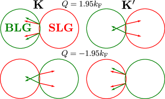
Thus a nonvanishing is possible depending on the pseudo-spin structure of the tunneling matrix , especially also for the case when pseudo-spin is conserved in a tunneling event (). That this must be the case can be explained based on the form of pseudo-spin states from the single-layer and the bi-layer-graphene system for which tunneling is allowed by simultaneous energy and momentum conservation. See Fig. 3. For example, as , the pseudo-spins of states at the ‘kissing’ point of the two Fermi circles become (oppositely) aligned in the () valley. Thus if the tunneling matrix is of the form , the overlap matrix elements (2) restrict tunneling to occur only for electrons from the valley. Conversely, if , pseudo-spin must be flipped in a tunneling event, and only electrons from the valley are able to accommodate that condition with simultaneous energy and momentum conservation. In both situations, the tunneling current will be fully valley-polarized as a result.
The tunneling current will be non-vanishing in general and can even be large under the same conditions that maximize . As an example, we provide the expression of the total tunneling conductance for the case when :
| (9) |
where is the effective mass of electrons in the graphene bi-layer Castro Neto et al. (2009), the Fermi velocity in the single layer Castro Neto et al. (2009), and the area of the tunnel-barrier interface between the vertically separated 2D conductors. Clearly, for the condition associated with 100% valley polarization of the tunneling current, there is a divergence in the total magneto-tunnelling conductance. 222In real samples, the finite electronic life time will smoothen this divergence into a Lorentzian peak. See, e.g., Ref. Jungwirth and MacDonald, 1996. Specializing , we can give the result
| (10) |
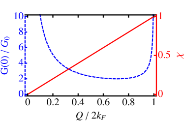
which further simplifies when to . See Fig. 4 for an illustration of the simultaneous occurrence of 100% valley polarization and maximum of tunneling transport, shown there for the special situation of equal densities in the two layers and a pseudo-spin-conserving tunnel barrier.
The efficiency of the valley-filtering device proposed here will be affected by the pseudo-spin structure of the tunnel barrier, which is determined by the geometric placement of the single and bi-layer sheets with respect to each other. Our previously suggested method Pratley and Zülicke (2013) to determine the full pseudo-spin structure of the tunnel coupling could be employed to optimize the vertical-heterostructure design in this regard. Furthermore, the valley polarization of the tunneling conductance is limited by the available magnitudes of the in-plane magnetic field. Using the case of equal density in the two layers and pseudo-spin-conserving tunneling as an example, we can estimate
| (11) |
Thus in-plane magnetic fields of the order of T are required to generate significant valley polarization in realistic vertical heterostructures of graphene layers.
In conclusion, we have studied tunneling transport between two parallel graphene sheets, one being a single-layer and the other a bi-layer sample. The requirement of simultaneous energy and momentum conservation, together with the distinctive valley-contrasting pseudo-spin-momentum locking in the two different graphene systems, causes a finite valley polarization of the tunneling current when an in-plane magnetic field is applied. For large-enough field magnitude, 100% valley polarization can be achieved, and a significant magnitude of polarization is generally realized concomitantly with large values of the total tunneling current.
In contrast to many other valley-filter designs, the vertical-tunneling-based proposal works without substantially altering the conducting properties of the graphene sheets. As a valley-polarized current is generated in the bulk, the present set-up is ideal for realizing valley-optoelectronic devices Yao, Xiao, and Niu (2008); Golub et al. (2011) as well as applications related to the valley-Hall effect Xiao, Yao, and Niu (2007) and its inverse. The fact that a valley polarization simultaneously exists in parallel single and bi-layer graphene sheets opens up possibilities for a three-dimensional valleytronic chip design.
Acknowledgments – LP gratefully acknowledges scholarship funding from Victoria University. Work at KITP was supported in part by the National Science Foundation under Grant No. NSF PHY11-25915.
References
- Žutić, Fabian, and Das Sarma (2004) I. Žutić, J. Fabian, and S. Das Sarma, Rev. Mod. Phys. 76, 323 (2004).
- Sinova and Žutić (2012) J. Sinova and I. Žutić, Nat. Mater. 11, 368 (2012).
- Weiss et al. (2012) N. O. Weiss, H. Zhou, L. Liao, Y. Liu, S. Jiang, Y. Huang, and X. Duan, Adv. Mat. 24, 5782 (2012).
- Pesin and MacDonald (2012) D. Pesin and A. H. MacDonald, Nat. Mater. 11, 409 (2012).
- Castro Neto et al. (2009) A. H. Castro Neto, F. Guinea, N. M. R. Peres, K. S. Novoselov, and A. K. Geim, Rev. Mod. Phys. 81, 109 (2009).
- Xiao, Yao, and Niu (2007) D. Xiao, W. Yao, and Q. Niu, Phys. Rev. Lett. 99, 236809 (2007).
- Rycerz, Tworzydło, and Beenakker (2007) A. Rycerz, J. Tworzydło, and C. W. J. Beenakker, Nat. Phys. 3, 172 (2007).
- Yao, Xiao, and Niu (2008) W. Yao, D. Xiao, and Q. Niu, Phys. Rev. B 77, 235406 (2008).
- Garcia-Pomar, Cortijo, and Nieto-Vesperinas (2008) J. L. Garcia-Pomar, A. Cortijo, and M. Nieto-Vesperinas, Phys. Rev. Lett. 100, 236801 (2008).
- Abergel and Chakraborty (2009) D. S. L. Abergel and T. Chakraborty, Appl. Phys. Lett. 95, 062107 (2009).
- Fujita, Jalil, and Tan (2010) T. Fujita, M. B. A. Jalil, and S. G. Tan, Appl. Phys. Lett. 97, 043508 (2010).
- Low and Guinea (2010) T. Low and F. Guinea, Nano Lett. 10, 3551 (2010).
- Zhai et al. (2010) F. Zhai, X. Zhao, K. Chang, and H. Q. Xu, Phys. Rev. B 82, 115442 (2010).
- Schomerus (2010) H. Schomerus, Phys. Rev. B 82, 165409 (2010).
- Wu et al. (2011) Z. Wu, F. Zhai, F. M. Peeters, H. Q. Xu, and K. Chang, Phys. Rev. Lett. 106, 176802 (2011).
- Gunlycke and White (2011) D. Gunlycke and C. T. White, Phys. Rev. Lett. 106, 136806 (2011).
- Golub et al. (2011) L. E. Golub, S. A. Tarasenko, M. V. Entin, and L. I. Magarill, Phys. Rev. B 84, 195408 (2011).
- Jiang et al. (2013) Y. Jiang, T. Low, K. Chang, M. I. Katsnelson, and F. Guinea, Phys. Rev. Lett. 110, 046601 (2013).
- Wu, Lue, and Chen (2013) G. Y. Wu, N.-Y. Lue, and Y.-C. Chen, Phys. Rev. B 88, 125422 (2013).
- Khatibi, Rostami, and Asgari (2013) Z. Khatibi, H. Rostami, and R. Asgari, Phys. Rev. B 88, 195426 (2013).
- Britnell et al. (2012a) L. Britnell, R. V. Gorbachev, R. Jalil, B. D. Belle, F. Schedin, A. Mishchenko, T. Georgiou, M. I. Katsnelson, L. Eaves, S. V. Morozov, N. M. R. Peres, J. Leist, A. K. Geim, K. S. Novoselov, and L. A. Ponomarenko, Science 335, 947 (2012a).
- Britnell et al. (2012b) L. Britnell, R. V. Gorbachev, R. Jalil, B. D. Belle, F. Schedin, M. I. Katsnelson, L. Eaves, S. V. Morozov, A. S. Mayorov, N. M. R. Peres, A. H. Castro Neto, J. Leist, A. K. Geim, L. A. Ponomarenko, and K. S. Novoselov, Nano Lett. 12, 1707 (2012b).
- Georgiou et al. (2012) T. Georgiou, R. Jalil, B. D. Belle, L. Britnell, R. V. Gorbachev, S. V. Morozov, Y.-J. Kim, A. Gholinia, S. J. Haigh, O. Makarovsky, L. Eaves, L. A. Ponomarenko, A. K. Geim, K. S. Novoselov, and A. Mishchenko, Nat. Nanotech. 8, 100 (2012).
- Britnell et al. (2013) L. Britnell, R. V. Gorbachev, A. K. Geim, L. A. Ponomarenko, A. Mishchenko, M. T. Greenaway, T. M. Fromhold, K. S. Novoselov, and L. Eaves, Nat. Commun. 4, 1794 (2013).
- Geim and Grigorieva (2013) A. K. Geim and I. V. Grigorieva, Nature (London) 499, 419 (2013).
- Myoung et al. (2013) N. Myoung, K. Seo, S. J. Lee, and G. Ihm, ACS Nano 7, 7021 (2013).
- Feenstra, Jena, and Gu (2012) R. M. Feenstra, D. Jena, and G. Gu, J. Appl. Phys. 111, 043711 (2012).
- Bala Kumar, Seol, and Guo (2012) S. Bala Kumar, G. Seol, and J. Guo, Appl. Phys. Lett. 101, 033503 (2012).
- Vasko (2013) F. T. Vasko, Phys. Rev. B 87, 075424 (2013).
- Pratley and Zülicke (2013) L. Pratley and U. Zülicke, Phys. Rev. B 88, 245412 (2013).
- Smoliner et al. (1989) J. Smoliner, W. Demmerle, G. Berthold, E. Gornik, G. Weimann, and W. Schlapp, Phys. Rev. Lett. 63, 2116 (1989).
- Eisenstein et al. (1991) J. P. Eisenstein, T. J. Gramila, L. N. Pfeiffer, and K. W. West, Phys. Rev. B 44, 6511 (1991).
- Hayden et al. (1991) R. K. Hayden, D. K. Maude, L. Eaves, E. C. Valadares, M. Henini, F. W. Sheard, O. H. Hughes, J. C. Portal, and L. Cury, Phys. Rev. Lett. 66, 1749 (1991).
- Gennser et al. (1991) U. Gennser, V. P. Kesan, D. A. Syphers, T. P. Smith, S. S. Iyer, and E. S. Yang, Phys. Rev. Lett. 67, 3828 (1991).
- Simmons et al. (1993) J. A. Simmons, S. K. Lyo, J. F. Klem, M. E. Sherwin, and J. R. Wendt, Phys. Rev. B 47, 15741 (1993).
- Zheng and MacDonald (1993) L. Zheng and A. H. MacDonald, Phys. Rev. B 47, 10619 (1993).
- Lyo and Simmons (1993) S. K. Lyo and J. A. Simmons, J. Phys.: Condens. Matter 5, L299 (1993).
- Raichev and Vasko (1996) O. E. Raichev and F. T. Vasko, J. Phys.: Condens. Matter 8, 1041 (1996).
- Jungwirth and MacDonald (1996) T. Jungwirth and A. H. MacDonald, Phys. Rev. B 53, 7403 (1996).
- Pershoguba and Yakovenko (2012) S. S. Pershoguba and V. M. Yakovenko, Phys. Rev. B 86, 165404 (2012).
- Note (1) This is based on the realistic assumption that the tunnel-barrier height is much larger than the bandwidth of relevant electronic excitations. In principle, the -dependence of can modify the density dependence of tunneling conductances but will not affect the functionality of our proposed valley-filter device.
- Note (2) In real samples, the finite electronic life time will smoothen this divergence into a Lorentzian peak. See, e.g., Ref. \rev@citealpnumjun96.