]http://www.m2netlab.wlu.ca
Coupled multiphysics, barrier localization, and critical radius effects in embedded nanowire superlattices
Abstract
The new contribution of this paper is to develop a cylindrical representation of an already known multiphysics model for embedded nanowire superlattices (NWSLs) of wurtzite structure that includes a coupled, strain dependent 8-band Hamiltonian in cylindrical coordinates and investigate the influence of coupled piezo-electromechanical effects on the barrier localization and critical radius in such NWSLs. The coupled piezo-electromechanical model for semiconductor materials takes into account the strain, piezoelectric effects and spontaneous polarization. Based on the developed 3D model, the band structures of electrons (holes) obtained from results of modeling in Cartesian coordinates are in good agreement with those values obtained from our earlier developed 2D model in cylindrical coordinates. Several parameters such as lattice mismatch, piezo-electric fields, valence and conduction band offsets at the heterojunction of supperlattice can be varied as a function of the Al mole fraction. When the band offsets at the heterojunction of are very small and the influence of the piezo-electromechanical effects can be minimized, then the barrier material can no longer be treated as an infinite potential well. In this situation, it is possible to visualize the penetration of the Bloch wave function into the barrier material that provides an estimation of critical radii of NWSLs. In this case, the NWSLs can act as inversion layers. Finally, we investigate the influence of symmetry of the square and cylindrical NWSLs on the band structures of electrons in the conduction band. However for larger lateral size of the NWSLs, the influence of such edge effects on the band structures of the NWSLs are not substantially influenced by the choice of either square or cylindrical symmetry but the localization of weavefunction with square symmetry is different than for the case with cylindrical symmetry which might indicate that the symmetry is broken in square shape NWSLs.
I Introduction
Studies on low dimensional systems, such as nanowires and superlattices, have attracted considerable attention, spurred on by the development of smaller and faster electronic devices and by the exploitation of their extraordinary properties for improved performance in various areas of science and technology, including nano- and micro-electronics, thermoelectricity and magnetism. Huang et al. (2001); Lin and Dresselhaus (2003); Venkatasubramanian et al. (2001); Harman et al. (2002); Nielsch et al. (2001); Prabhakar et al. (2013) Today’s technology allows finite length modulated quantum wire heterostructures to be grown in what is known as NWSLs. NWSLs are the nanoscale building blocks that through the bottom up assembly can enable diverse applications. One can expect a straightforward analogy to the planar electronic/optoelectronic industry to extrapolate that complex compositionally modulated superlattice structures could greatly increase the versatility and power of these building blocks in nanoscale applications. Huang et al. (2002)
In the NWSLs, the localization in barriers and the critical radius are important issues. Chuang et al. (2007); Cirlin et al. (2009); Raychaudhuri and Yu (2006) The existence of barrier localization and the calculation of critical radius in NWSLs have been previously carried out by using one band effective mass theory in Refs. Voon et al., 2004; Willatzen et al., 2004. Those earlier results indicated the possibility of these modulated structures to display free carrier like behavior along the nanowire axis when a critical wire radius is considered. Moreover, it has been shown that the existence of critical radii for inversion of state localization is a much more general phenomenon. Most of these studies deal with free standing NWSLs. The barrier localization and critical radius phenomena can be particularly important in AlGaN/GaN NWSLs where band structure parameters can be controlled with the variation of Al mole fraction. In this situation, the influence of piezo-electromechanical effects can be minimized. As a result, we see the penetration of the wavefunctions into the barrier materials which provides the evidence of the presence of critical radii in the NWSLs. Voon et al. (2004); Voon and Willatzen (2003)
II Piezo-electromechanical effects
II.1 Piezo-electromechanical effects in Cartesian coordinates
To investigate the influence of piezo-electromechanical effect on the band structure calculation of low dimensional semiconductor nanostructures, following Refs. Lassen et al., 2008, first we write the coupled system of the Navier equations for stress and Maxwel’s equations for piezoelectric fields as Melnik (2000); Prabhakar et al. (2012a)
| (1) | |||
| (2) |
The stress tensor components and the electric displacement vector components can be written as Barettin et al. (2008); Lassen et al. (2008)
| (3) | |||
| (4) |
where are the elastic moduli constants, is the piezoelectric constant, is the permittivity, is the piezoelectric potential, is the spontaneous polarization and is the built in piezoelectric potential. Also, are the components of strain tensors which are written as
| (5) |
where are the local intrinsic strain tensor components due to lattice mismatch and is position dependent strain tensor components. These two can be written as
| (6) | |||
| (7) |
where and are the local intrinsic strains along a- and c-directions, respectively (which are nonzero in the quantum well and zero otherwise). Here, , and , are the lattice constants of the quantum well and the barrier material of the NWSLs.
II.2 Piezo-electromechanical effects in cylindrical coordinates
In cylindrical polar coordinates (), Eqs. (3) and (4) can be written as Melnik (2000); Barettin et al. (2008); Prabhakar and Melnik (2010); Patil and Melnik (2009)
| (8) | |||
| (9) | |||
| (10) | |||
| (11) | |||
| (12) | |||
| (13) |
Also, the coupled equations of wurtzite structure in the presence of piezo-electromechanical effects in cylindrical coordinates can be written as Melnik (2000)
| (14) | |||
| (15) | |||
| (16) |
From Eqs. 8 to 13, the components of the strain tensor, expressed through the displacement vector , for which , are
| (17) | |||
| (18) |
The strain tensor components and the piezoelectric field (potential) can be found by solving the electroelasticity problem (14), (15) and (16).
III Band structure calculations
III.1 8-band model in Cartesian coordinates
The steady state Schrödinger equation of the Kane model for the electrons in the conduction band and holes in the valence band can be written as Kane (1957); Bir and Pikus. (1974); Löwdin (1951); Rinke et al. (2008); Fu and Wu (2008); Prabhakar et al. (2012a)
| (19) |
where
| (20) |
with and are the position dependent conduction and valence band envelope functions.
The total wave function is: Winkelnkemper et al. (2006); Prabhakar et al. (2012a)
| (21) |
where and . The functions are spinless and is a spinor:
| (22) |
Hence, the basis functions of the Hamiltonian (20) take the following form: Winkelnkemper et al. (2006); Prabhakar et al. (2012a)
We now turn to the description of the matrix Hamiltonian of (20). The diagonal element of the conduction band Hamiltonian can be written as
| (23) | |||||
where is the position dependent edge of the conduction band , and are deformation potentials for the conduction band. The parameters and are expressed via the components and of the tensor of the reciprocal effective masses for the conduction band in the single-band approximation and the Kane parameters and . They are given by Winkelnkemper et al. (2006); Prabhakar et al. (2012a)
| (24) | |||
| (25) |
where is the band gap of semiconductor materials.
The intra-valence-band Hamiltonian can be written as
| (26) |
The Hamiltonian entering Eq. (26) represents the position-dependent potential energy of an electron:
| (27) |
where and are the position dependent edges of the valence bands and , respectively.
The spin-orbit Hamiltonian in Eq. (26) can be treated as a perturbation term and can be written as Chuang and Chang (1996); Bir and Pikus. (1974)
| (28) |
where and are the parameters of the valence-band spin-orbit splitting and are the Pauli spin matrices:
| (29) |
The kinetic energy Hamiltonian in Eq. (26) can be written as Winkelnkemper et al. (2006)
| (30) |
where
| (31) | |||
| (32) |
Also,
| (33) |
with , , … being real material parameters in conventional notations Chuang and Chang (1996); Bir and Pikus. (1974); Winkelnkemper et al. (2006), is the free electron mass. Wurtzite structure has six fold rotational symmetry and thus we use the relation .
Finally, the strain tensor components are written as Fonoberov and Balandin (2003)
| (34) |
where material constants , , , , and are expressed via conventional deformation potential tensor components as follows: Bir and Pikus. (1974); Chuang and Chang (1996); Winkelnkemper et al. (2006)
| (35) |
We can also apply six fold rotational symmetry in the strain Hamiltonian of wurtzite structure which holds the relation .
III.2 8-band model in cylindrical coordinates
To derive the strain dependent 8-band model in cylindrical coordinates , with and , we introduce two different unitary matrices as Prabhakar et al. (2012b); Takhtamirov and Melnik
| (38) |
| (39) |
We rotate the strain dependent 8-band Hamiltonian (19) by . We follow here the ideas first published in Ref. Prabhakar et al., 2012b; Takhtamirov and Melnik, . Thus, the eigenvalue problem (19) can be written as
| (40) |
In Eq. 40, we introduce new basis functions , where
| (41) |
Note that the new basis functions are invariant under the rotation of the Cartesian coordinate system around the z-axis i.e., . It can be seen that and do not obey the periodicity properties of the functions and and thus they are not the Bloch functions at this moment. The total wavefunction and the envelope functions are related to each other through conventional basis functions or the modified functions () as follows:
| (42) |
Earlier we have noticed that and are not periodic and they are not Bloch functions so it is convenient to retain the old basis functions which are periodic and orthonormal. Thus, we obtain the old envelope functions as
| (43) |
To transform the Hamiltonian (20) (), we use the following identities:
| (44) |
as well as the relations
| (45) |
We obtain the elements of (see 30) as follows:
| (46) | |||||
| (47) | |||||
| (48) | |||||
The rest of the elements are obtained analogously. Thus the full matrix of the kinetic energy Hamiltonian (30) in the rotated frame can be written as:
| (49) |
Note that and thus the Hamiltonian (49) is Hermitian. It can be seen that Hamiltonian (49) resembles the one in Refs. Voon et al., 2005 with different coefficients due to the fact that our choice of the basis functions and unitary rotation matrix are different. Takhtamirov and Melnik Since (see 54) will contain that does not commute with the operator , we need to perform another set of rotation to remove the dependency from . Thus it is also required to find all the elements of under the rotation . Again, by performing another lengthy algebraic transformations, we obtain the elements of (see (20)). For example, of Eq. (23) can be written as
| (50) | |||||
where we use the identity:
| (51) | |||||
Similarly, of Eq. (37) can be written as
| (52) |
Also, first element of in (30) can be written as
| (53) |
In a similar fashion, one can find the rest of the elements of strain dependent 8-band Hamiltonian in cylindrical polar coordinates (). The results of this procedure were first reported in Ref. Prabhakar et al., 2012b.
Following it, we can transform the spin-orbit interaction Hamiltonian (28) as , where . Thus we can write
| (54) |
where and .
Notice that the spin-orbit Hamiltonian (54) depends on which does not commute with the operator . To avoid this dependence, we note that
| (55) |
and then the spin-orbit interaction Hamiltonian transforms into its initial form (28):
| (56) |
For cylindrically symmetric systems, the total rotated Hamiltonian commutes with the z-component of the total angular momentum operator . These two commuting operators have the common eigenfunctions so that the total rotated envelope functions can be chosen in the form of
| (57) |
where are the eigenvalues of the z-components of the total angular momentum . The advantages of using these basis functions (57) in the rotated frame is that the total Hamiltonian becomes independent from the strain dependent 8-band Hamiltonian.
Now we summarize the strain dependent 8-band Hamiltonian in cylindrical coordinates as follows:
| (58) |
where and the matrix has the form:
| (59) |
By identifying (see Eqs. 17 and 18) in cylindrical coordinates, we verified that the total strain dependent 8-band Hamiltonian (58) in cylindrical coordinates are rotationally invariant with respect to the rotation around the c-axis.
IV Computational Method:
We have used the Finite Element Method (FEM) com and solve the corresponding eigenvalue problem of fully strain dependent 8-band Hamiltonian in 3D Cartesian coordinates and in 2D cylindrical coordinates. For 3D solutions (both electromechanical and band structure calculations), we have imposed Neumann boundary conditions i.e., the continuity equation must hold at the heterojunction which is also referred to as the internal boundaries. Dirichlet boundary conditions are imposed on the rest of the boundary. For cylindrically symmetric 2D model, we define the z axis to be perpendicular to the plane of the quantum-well layer and r axis that lies in the quantum-well plane. For electromechanical parts, we have imposed , and along the symmetry axis (i.e., at r=0) (for details, see Ref. Barettin et al., 2008). Here, we also impose Neumann boundary conditions at the internal boundaries and Dirichlet boundary conditions at the rest of the boundary. For the band structure calculations of 2D cylindrical nanowires, we have imposed Neumann boundary conditions along the symmetry axis as well as at the internal boundaries. We have imposed Dirichlet boundary conditions at the rest of the boundary by assuming that the total Hamiltonian of the nanowire is rotationally invariant around z-direction. Finally, in 3D Cartesian coordinates and in 2D cylidnrical coordinates, we have used the corresponding normalization conditions
| (60) | |||
| (61) |
The materials constants for our computation are taken from Refs. Prabhakar et al., 2012a; Komirenko et al., 1999; Vurgaftman and Meyer, 2003 and listed in tables 1 and 2.
| Parameter | GaN | AlN |
|---|---|---|
| (eV) | 3.51 | 6.25 |
| (eV) | 0.034 | -0.295 |
| (eV) | 0.017a | 0.019a |
| 0.19 | ||
| 0.21 | ||
| -5.947 | ||
| -0.528 | ||
| 5.414 | ||
| -2.512 | ||
| -2.510 | ||
| -3.202 | ||
| (eVÅ) | 0.046 | |
| (eVÅ) | 8.1 | |
| (eVÅ) | 7.9 | |
| (eV) | -4.9a | -3.4a |
| (eV) | -11.3a | -11.8a |
| (eV) | -3.7a | -17.1a |
| (eV) | 4.5a | 7.9a |
| (eV) | 8.2a | 8.8a |
| (eV) | -4.1a | -3.9a |
| (eV) | -4.0a | -3.4a |
| (eV) | -5.5a | -3.4a |
aRef. Vurgaftman and Meyer, 2003.
V Results and Discussions
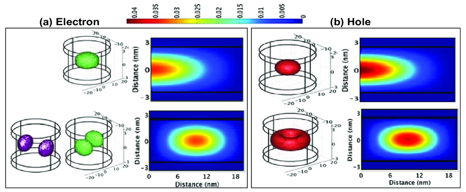
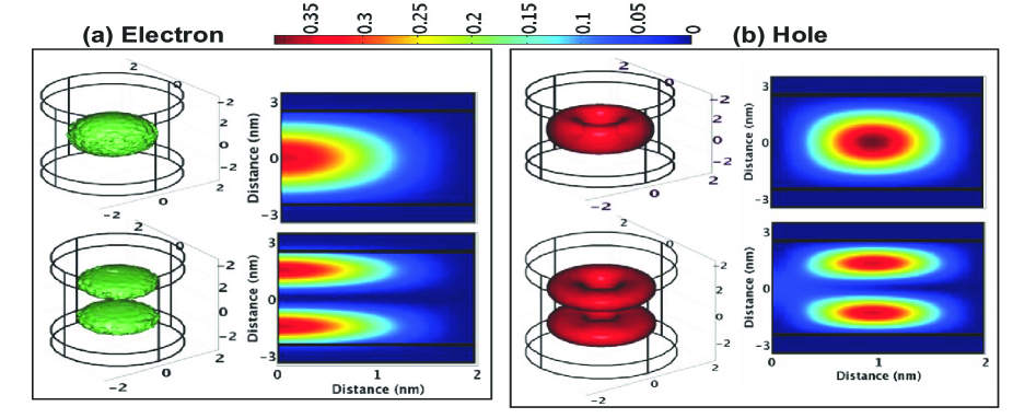
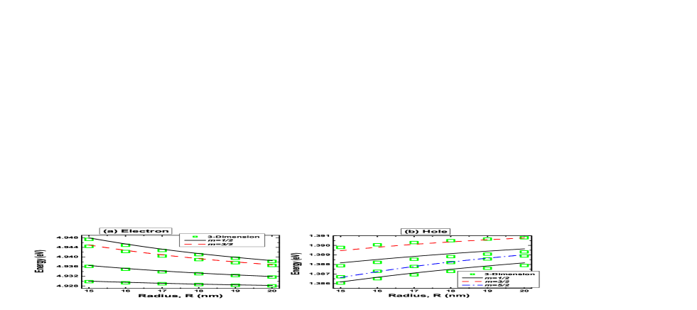
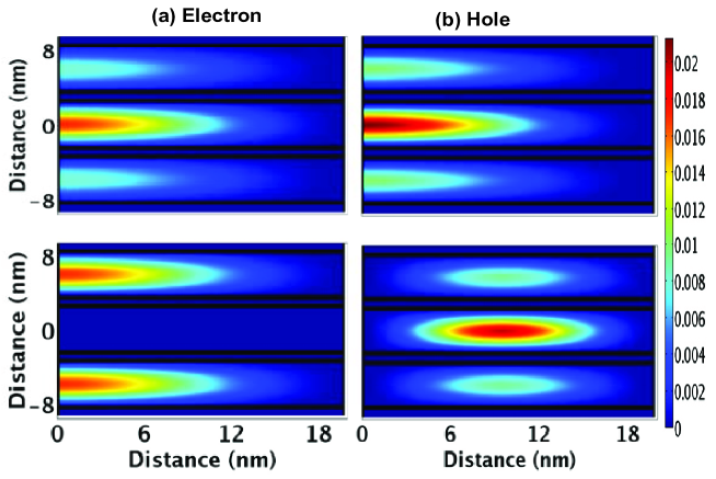
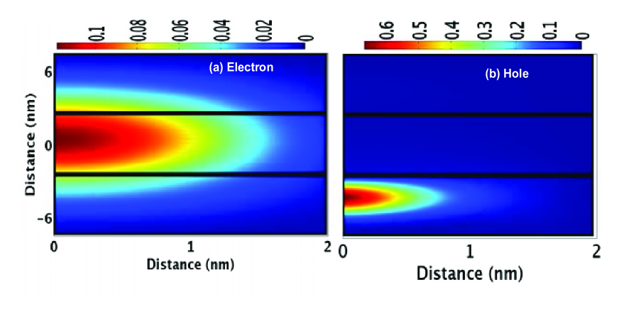
We have plotted probability distributions of the ground and first excited states of electrons and holes in Fig. 1(a) and Fig. 1(b), respectively. Here we consider the radius of the AlN/GaN/AlN nanowire as 20 nm. Also, in Fig. 2(a) and Fig. 2(b), we have plotted probability distributions of the ground and first excited states of electrons and holes where the radius of the AlN/GaN/AlN NWSLs was only 2 nm in order to investigate the radial influence of the localization of the electron and hole wavefunctions. By comparing the distribution functions of the ground state of electron in Fig. 1(a) for R=20 nm and in Fig. 2(a) for R=2 nm, we have found the maximum probability point at (r,z)=(0,0). However, for the excited states, we have found the zero probability point at and maximum probability points at . Also for hole states, we have found the maximum probability point at (r,z)=(0,0) for the ground state wavefunction in Fig.1(b) (R=20 nm) and zero probability point at for the ground state wavefunction in Fig.2(b) (R=2 nm). However, for hole excited states, we have found the zero probability point at and two zero probability points at . In Fig. 3, we compare several eigenvalues of electron and hole states obtained from the 3D model in Cartesian coordinates to those values obtained from the 2D model in cylindrical coordinates. It can be seen that the eigenvalues obtained from the 3D and 2D models are in excellent agreement with difference less than . The numerical error is due to the FEM implementation and can be reduced further by refining the mesh in 3D. This comparison of eigenvalues in 3D and 2D models demonstrates that the derived 8-band model in cylindrical coordinates can be used for NWSLs instead of general 3D model. This substantially reduces the required computational time. Notice that for the holes in the valence band, the lowest state of corresponds to the ground state (see dashed line (red) in Fig. 3(b)) and the lowest state of corresponds to the first excited state (see solid line (black) in Fig. 3(b)). In Ref. Lew Yan Voon et al., 2004, the Sercel-Vahala basis Sercel and Vahala (1990) was used for the model reductions in the case of cylindrical coordinates. The methodology proposed in this paper is different. Based on Fig. 5, we further analyze the differences between these two approaches for NWSLs with small radii. Comparisons between 3D and 2D models are reported for the first time here for NWSLs, but the developed 8-band model in cylindrical coordinates is applicable also to cylindrical quantum dots and other low dimensional nanostructures with cylindrical geometry as long as the systems are invariant around c-axis. In Fig. 4, we have potted the probability distributions of ground and first excited states of electrons and holes in three layers of AlN/GaN NWSLs. We again have found that the maximum probability point for the ground state wavefunctions of electrons and holes are at (r,z)=(0,0).
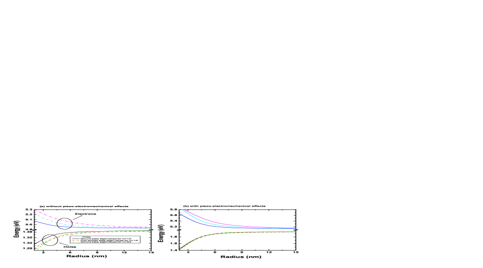
In Fig. 5, we investigate the influence of piezo-electromechanical effects on the band structure calculations of electrons and holes in cylindrical AlN/GaN/AlN NWSLs (Figs. 5(a) and (b) present the results without and with pizo-electromechanical effects, respectively). We have substituted in (58) and found the ground, first, second and so on excited states of electrons in the conduction bands. We confirm that for electrons in the conduction band, first excited states of correspond to the ground state of and second excited states of correspond to the ground states of and so on. For holes in the valence band in Fig. 5(a), we demonstrate the finite radius influence at nm where we find the crossing of the eigenstates between the lowest states of m=1/2 and m=3/2. This indicates that for nm, the lowest state eigenvalue with m=1/2 corresponds to the ground state and the lowest state eigenvalue with corresponds to the first excited state. These results have not been previously reported.
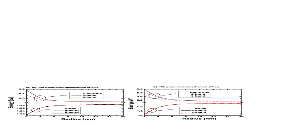
In Fig. 6, we provide additional justification of utilizing 8-band Hamiltonian in wide band gap AlN/GaN/AlN NWSLs. We compare the ground state eigenvalues obtained from the 8-band Hamiltonian to those of decoupled 2-conduction and 6-valence bands envelope function methods. We see that the band structures of holes obtained from 6-bands and 8-bands Hamiltonian both provide correct estimations. However, for electrons in the conduction band, the influence of non-parabolicity term (i.e., when including realistic values of and ) in the effective mass approximation in the 8-band Hamiltonian induces a significant contribution to the band structure of wide band gap AlN/GaN/AlN NWSLs. By substituting in (58), one can find decoupled 2-conduction and 6-valence band Hamiltonians. In Fig. 6 (b), we have included the piezo-electromechanical effect and shown that the energy difference between the ground state eigenvalues of 2-band and 8-band is enhanced. Further enhancement can be achieved if we bring the minima and maxima of the conduction and valence bands closer with the application of the gate controlled electric fields along z-direction. Prabhakar et al. (2012a)
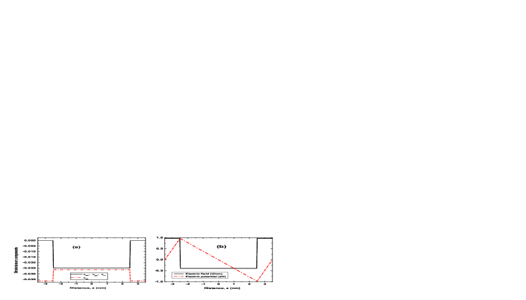
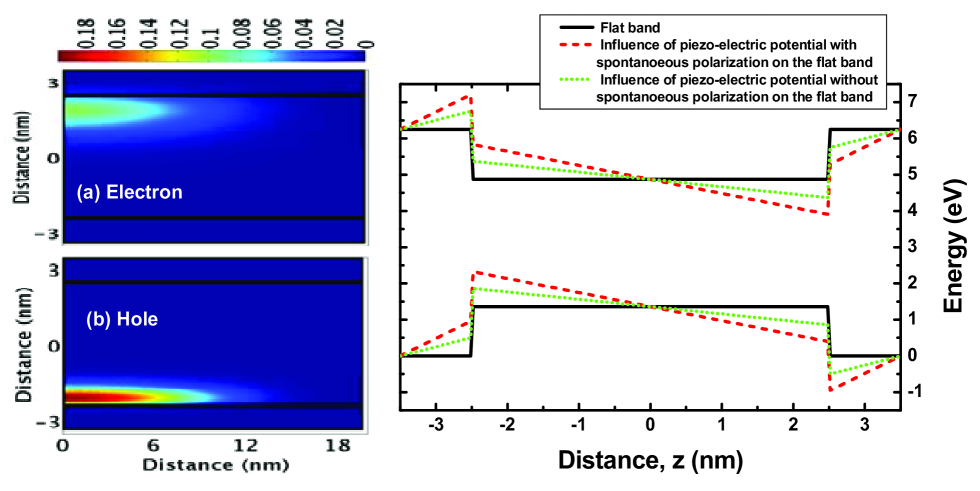
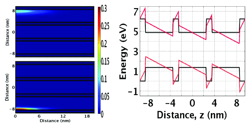
Bulk GaN and AlN have different lattice constants so when (0001) GaN NWSLs structure is grown, a significant lattice mismatch occurs at the interface between the GaN wells and AlN barriers. Chuang and Chang (1996); Barettin et al. (2008); Patil and Melnik (2009) The strain induced polarization along z-direction results in strong built in piezoelectric fields and increased potential along z-direction. We solve the Navier equations (1) for stress and Maxwel’s equations (2) for piezoelectric fields in 3D on the one hand, and 2D coupled Eqs. (14), (15) and (16) in cylindrical coordinates on the other hand, to investigate the piezo-electromechanical effects in wurtzite AlN/GaN/AlN (single layer of GaN) QWs. We assumed pseudomorphic strain conditions and plotted the nonvanishing position dependent strain tensor comments (, , , ) in Fig. 7(a) and electric field and potential in Fig. 7(b) as a function of position along the z-direction. In Fig. 8, we investigate the influence of piezo-electromechanical effects on the band structure calculation of wurtzite AlN/GaN NWSLs. We see that the influence of piezo-electromechanical effect pushes the minima of the conduction band at the top of the well and also pushes the maxima of the valence band at the bottom of the well. As a result, we find the localization of the electron wavefunction at the top of the well and hole wavefunction at the bottom of the well. In Fig. 9, we investigate the influence of piezo-electromechanical effects on the band structure calculation of wurtzite AlN/GaN multi layers of NWSLs. Here again, we see that the wavefunction of electrons in the conduction band is localized at the top of the GaN QW in the upper layer of the NWSLs and the hole wavefunction is localized at the bottom of the GaN QW in the lower layer of the NWSLs.
We now turn to another key result of the paper: critical radius and quantum confinement in wurtzite NWSL structures.
The critical radius () corresponds to those values of the radius of NWSLs for which the localization of the wavefunction penetrates into the barrier materials. For instance, if , the localization of the wavefunction resides within the QW materials. In AlN/GaN NWSLs, the AlN barrier material acts as an infinite potential wall where the penetration of the wavefunction into the barrier material is not possible. However, if we reduce the Al mole fraction in NWSLs, we also reduce the band offsets i.e., the barrier height of electrons (holes) is reduced at the interface of the heterojunction. In this situation, the influence of piezo-electromechanical effects is minimized and the penetration of electron (hole) wavefunctions can be seen to the barrier materials. In a simple one band model within the effective mass approximation, the authors in Ref. Voon et al., 2004 provided the mathematical condition for the critical radius as
| (62) |
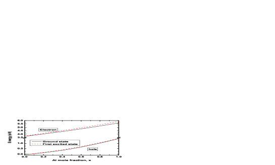
where is the zero of the Bessel function, is the barrier height and , correspond to the effective masses of electron (hole) in the barrier and in the well. For with , we find , and for electrons in the conduction band which gives . In Fig. 10, we plotted the ground state wavefunction of electrons (Fig. 10(a)) and holes (Fig. 10(b)) in the conduction and valence bands respectively for the radius . Notice that the wavefunctions of electrons and holes spread into the barrier materials ( with ). In Fig. 11, we plotted the energy level diagram of ground and first excited states of electrons and holes as a function of Al mole fraction. As we increase the Al mole fraction in NWSLs, we also enhance the influence of piezo-electromechanical effects. As a result, the subband energy difference between ground and first excited states of electron (hole) states also increases.
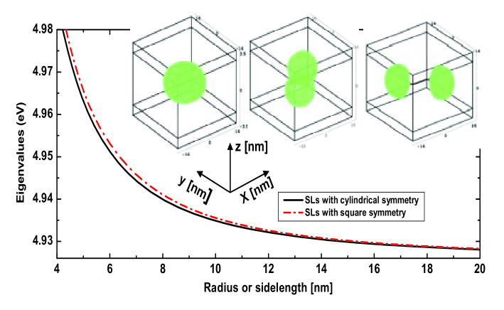
Finally, in Fig. 12, we compare the band structures of AlN/GaN/AlN NWSLs of cylindrical and square symmetry. We consider the volume of the square and cylindrical NWSLs to be the same (i.e., , where is the side length of the square NWSLs and is the radius of the cylindrical NWSLs). For smaller values of or , the localized states are formed very close to the edge and thus we find the larger eigenvalues for the NWSLs of square symmetry. However, for larger values of or , the localized states are formed far away from the edge in both types of cylindrical and square NWSLs and thus we find the eigenvalues are not substantially influenced by the choice of either square or cylindrical symmetry. In this case, the localization of first excited state weavefunction with square symmetry (inset plot of Fig. 12) is different from the case with cylindrical symmetry (Fig. 1 (a) lower panel) which might indicate that the symmetry is broken in square shape NWSLs.
VI Conclusions
By applying rotationally invariant basis functions with appropriate unitary transformation, we have formulated and applied the strain dependent 8-band Hamiltonian in cylindrical coordinates. This approach allows us to find the band structures of low dimensional semiconductor nanostructures in a computationally efficient way. This includes quantum dots, quantum wells or nanowire supperlattices as long as the systems are cylindrically symmetric along z-direction. We have provided the detailed analysis of the eigenvalues of electron (hole) states of wurtzite NWSLs for both 3D (Cartesian coordinates) and 2D (cylindrical coordinates) models. In a single and vertically stacked multiple layer of NWSLs, we have shown that the piezo-electromechanical effects push the electron wavefunction to the top of quantum well, while they push the hole wavefunction to the bottom of the well. We have shown that the influence of piezo-electromechanical effects in structures can be minimized by varying the Al mole fraction. In a situation, where the radius of the NWSL is very small compared to the critical radius, the localization of the electron (hole) wavefunction spreads into the barrier material. In this case, the barrier materials act as an inversion layer. Finally, we have shown the edge of the square symmetry enhances the eigenvalues of the localized states for smaller values of the side length of of the square NWSLs. For large NWSLs, we have shown that the eigenvalues of the localized states of square and cylindrical NWSLs is not substantially influenced by the edge states but the localization of weavefunction with square symmetry is different than for the case with cylindrical symmetry which might indicate that the symmetry is broken in square shape NWSLs.
The authors acknowledge Dr. Sunil Patil for his input on the initial version of this paper. This work was supported by Natural Sciences and Engineering Research Council (NSERC) of Canada and Canada Research Chair (CRC) programs.
References
- Huang et al. (2001) Y. Huang, X. Duan, Y. Cui, L. J. Lauhon, K.-H. Kim, and C. M. Lieber, Science 294, 1313 (2001).
- Lin and Dresselhaus (2003) Y.-M. Lin and M. S. Dresselhaus, Phys. Rev. B 68, 075304 (2003).
- Venkatasubramanian et al. (2001) R. Venkatasubramanian, E. Siivola, T. Colpitts, and B. O’Quinn, Nature 413, 597 (2001).
- Harman et al. (2002) T. C. Harman, P. J. Taylor, M. P. Walsh, and B. E. LaForge, Science 297, 2229 (2002).
- Nielsch et al. (2001) K. Nielsch, R. B. Wehrspohn, J. Barthel, J. Kirschner, U. Gösele, S. F. Fischer, and H. Kronmüller, Applied Physics Letters 79, 1360 (2001).
- Prabhakar et al. (2013) S. Prabhakar, R. V. Melnik, P. Neittaanmki, and T. Tiihonen, Journal of Computational and Theoretical Nanoscience 10, 534 (2013).
- Huang et al. (2002) Y. Huang, X. Duan, Y. Cui, and C. M. Lieber, Nano Letters 2, 101 (2002).
- Chuang et al. (2007) L. C. Chuang, M. Moewe, C. Chase, N. P. Kobayashi, C. Chang-Hasnain, and S. Crankshaw, Applied Physics Letters 90, 043115 (2007).
- Cirlin et al. (2009) G. E. Cirlin, V. G. Dubrovskii, I. P. Soshnikov, N. V. Sibirev, Y. B. Samsonenko, A. D. Bouravleuv, J. C. Harmand, and F. Glas, physica status solidi (RRL) Rapid Research Letters 3, 112 (2009).
- Raychaudhuri and Yu (2006) S. Raychaudhuri and E. T. Yu, Journal of Applied Physics 99, 114308 (2006).
- Voon et al. (2004) L. C. L. Y. Voon, B. Lassen, R. Melnik, and M. Willatzen, Journal of Applied Physics 96, 4660 (2004).
- Willatzen et al. (2004) M. Willatzen, R. Melnik, C. Galeriu, and L. L. Y. Voon, Mathematics and Computers in Simulation 65, 385 (2004).
- Voon and Willatzen (2003) L. C. L. Y. Voon and M. Willatzen, Journal of Applied Physics 93, 9997 (2003).
- Lassen et al. (2008) B. Lassen, M. Willatzen, D. Barettin, R. V. N. Melnik, and L. C. L. Y. Voon, Journal of Physics: Conference Series 107, 012008 (2008).
- Melnik (2000) R. V. N. Melnik, Applied Mathematics and Computation 107, 27 (2000).
- Prabhakar et al. (2012a) S. Prabhakar, R. V. Melnik, P. Neittaanmäki, and T. Tiihonen, Physica E: Low-dimensional Systems and Nanostructures 46, 97 (2012a).
- Barettin et al. (2008) D. Barettin, B. Lassen, and M. Willatzen, Journal of Physics: Conference Series 107, 012001 (2008).
- Prabhakar and Melnik (2010) S. Prabhakar and R. Melnik, Journal of Applied Physics 108, 064330 (2010).
- Patil and Melnik (2009) S. R. Patil and R. V. N. Melnik, Nanotechnology 20, 125402 (2009).
- Kane (1957) E. O. Kane, Journal of Physics and Chemistry of Solids 1, 249 (1957).
- Bir and Pikus. (1974) G. Bir and G. Pikus., Symmetry and strain induced effects in semiconductors (Wiley, 1974).
- Löwdin (1951) P.-O. Löwdin, The Journal of Chemical Physics 19, 1396 (1951).
- Rinke et al. (2008) P. Rinke, M. Winkelnkemper, A. Qteish, D. Bimberg, J. Neugebauer, and M. Scheffler, Phys. Rev. B 77, 075202 (2008).
- Fu and Wu (2008) J. Y. Fu and M. W. Wu, Journal of Applied Physics 104, 093712 (2008).
- Winkelnkemper et al. (2006) M. Winkelnkemper, A. Schliwa, and D. Bimberg, Phys. Rev. B 74, 155322 (2006).
- Chuang and Chang (1996) S. L. Chuang and C. S. Chang, Phys. Rev. B 54, 2491 (1996).
- Fonoberov and Balandin (2003) V. A. Fonoberov and A. A. Balandin, Journal of Applied Physics 94, 7178 (2003).
- Prabhakar et al. (2012b) S. Prabhakar, E. Takhtamirov, and R. Melnik, Acta Physica Polonica-Series A General Physics 121, 85 (2012b).
- (29) E. Takhtamirov and R. Melnik, arXiv: 1107.1285v1 .
- Voon et al. (2005) L. C. L. Y. Voon, C. Galeriu, B. Lassen, M. Willatzen, and R. Melnik, Applied Physics Letters 87, 041906 (2005).
- (31) Comsol Multiphysics version 3.5a (www.comsol.com).
- Komirenko et al. (1999) S. M. Komirenko, K. W. Kim, M. A. Stroscio, and M. Dutta, Phys. Rev. B 59, 5013 (1999).
- Vurgaftman and Meyer (2003) I. Vurgaftman and J. R. Meyer, Journal of Applied Physics 94, 3675 (2003).
- Lew Yan Voon et al. (2004) L. C. Lew Yan Voon, R. Melnik, B. Lassen, and M. Willatzen, Nano Letters 4, 289 (2004).
- Sercel and Vahala (1990) P. C. Sercel and K. J. Vahala, Phys. Rev. B 42, 3690 (1990).