Angular and Polarization Response of Multimode Sensors
with Resistive-Grid Absorbers
Abstract
High sensitivity receiver systems with near ideal polarization sensitivity are highly desirable for development of millimeter and sub-millimeter radio astronomy. Multimoded bolometers provide a unique solution to achieve such sensitivity, for which hundreds of single-mode sensors would otherwise be required. The primary concern in employing such multimoded sensors for polarimetery is the control of the polarization systematics. In this paper, we examine the angular- and polarization- dependent absorption pattern of a thin resistive grid or membrane, which models an absorber used for a multimoded bolometer. The result shows that a freestanding thin resistive absorber with a surface resistivity of , where is the impedance of free space, attains a beam pattern with equal - and -plane responses, leading to zero cross polarization. For a resistive-grid absorber, the condition is met when a pair of grids is positioned orthogonal to each other and both have a resistivity of . When a reflective backshort termination is employed to improve absorption efficiency, the cross-polar level can be suppressed below dB if acceptance angle of the sensor is limited to . The small cross-polar systematics have even-parity patterns and do not contaminate the measurements of odd-parity polarization patterns, for which many of recent instruments for cosmic microwave background are designed. Underlying symmetry that suppresses these cross-polar systematics is discussed in detail. The estimates and formalism provided in this paper offer key tools in the design consideration of the instruments using the multimoded polarimeters.
I Introduction
Present astronomical instrumentation applications in the millimeter and sub-millimeter desire photon backgrounded limited sensitivities. There are two possible basic approaches to further improve the sensitivity by increasing the number of detected spatial modes received by an imaging system. The first is to build an array consisting of numerous single-mode sensors with high optical efficiency. The second, a multi-mode sensor, detects many spatial modes on a single sensor (see, e.g., Ref. 1981IJQE...17..407R) with well-defined angular and polarization characteristics. In astronomical observations, for example, both single-mode sensors and multimoded sensors (see, e.g., Refs. Benford2008; Lawrence2008) have found wide use for radiometry and photometry.
Various techniques can be used to specify the modes coupled to a sensor and the resulting system architectures can be categorized by their modal filtering techniques (Fig. 1). In the context of polarimetry at millimeter wavelengths, where a significant use is for measuring the cosmic microwave background (CMB), the primary focus of the recent developments has been directed at large arrays of single-mode detectors with feed-coupled waveguide polarization diplexers 2009AIPC.1185..494E; 2010SPIE.7741E..51N; CLASS.SPIE.2012; 2009AIPC.1185..511M or planar-antenna coupled structures 2010SPIE.7741E..40O; 2010SPIE.7741E..50S; 2011AA...536A...1P; POLAR.SPIE.2012; 2010SPIE.7741E..39A; 2008SPIE.7010E..79C which can be photolithographically produced in large numbers. Here, polarization diplexing is achieved on the detector chip for the horizontal and vertical single mode detector channels (Fig. 1, S3). Prior to these developments, dual-mode waveguide-based orthomode transducer (OMT) structures followed by single-mode detectors 2003ApJS..145..413J; 2013ApJ...768....9B; Clover2009 were used to form a polarimeter following the traditions of microwave design. Alternatively, single-mode dual-polarization sensors were realized by combining intrinsically multimoded polarization-sensitive bolometers (PSBs) with external modal filtering structures to define the angular acceptance (Fig. 1, S2) 2007A&A...470..771J; 2010ApJ...711.1141T; 2008ApOpt..47.5996H; 2009ApJ...692.1221H. Multimoded sensors for imaging have also achieved polarization sensitivity through a wire-grid analyzer 1997PASP..109..307S; 2005ASPC..343...69B; 2006SPIE.6275E..48L; 2010SPIE.7741E..49B (Fig. 1, M1 and MP1). The analyzer grid architecture has also been employed in conjunction with a feed coupled array (e.g., Ref. 2004SPIE.5543..320O) to cleanly provide polarization sensitivity (Fig. 1, S1).
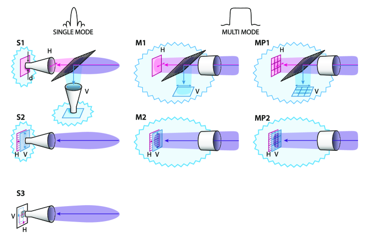
A multimoded bolometric sensor that is intrinsically polarization selective, as opposed to those using the wire-grid analyzer, belongs to another class of sensors and opens up a new phase space for polarization sensitive instruments in millimeter wavelength (Fig. 1, M2 and MP2). Such a bolometer would employ a thin resistive grid as a polarization selective absorber. An M2 implementation is the sensor developed for PIXIE satellite mission proposal aimed at CMB polarization and frequency spectrum measurements 2011JCAP...07..025K. This sensor employs a pair of orthogonally positioned resistive grids, each of which is separately read out, attaining simultaneous sensitivity to two linear polarizations. Other applications exploiting the unique features of this sensor are also proposed doi:10.1117/12.926271. An MP2 implementation, an intrinsically polarization-selective sensor based on a pair of filled arrays, was explored in Ref. 2006SPIE.6275E..27W where each detector absorber on a side was realized from a patterned thin metal film on a Si membrane and spaced by microns (Fig. 1, MP2). These types of sensors (M2 and MP2), similarly to M1 and MP1, require cold baffling to control the detector power loading, but share an improved mapping speed advantage compared to the single-mode sensors 2002ApOpt..41.6543G.
The focus of this paper is to provide an estimate of the angular- and polarization-dependent response pattern of the thin resistive absorber, and to show that bolometers corresponding to the M2 type in Fig. 1 can achieve low levels of polarization beam systematics. Further, the residual non-zero systematics are shown to have even-parity patterns. A potential use for these sensors is to probe the signature of the inflation in the early universe through the odd-parity, or so-called -mode, patterns in the CMB polarization 1997PhRvL..78.2054S; 1997PhRvL..78.2058K, which is not contaminated by the even-parity beam systematics 2003PhRvD..67d3004H; 2008PhRvD..77h3003S. Implications presented in this paper are general and applicable to a wide range of devices using thin absorbing grids or membranes, even though our work is motivated by the specific implementation of the device mentioned above 2011JCAP...07..025K; doi:10.1117/12.926271. We choose to analytically study this system – for numerical investigations the approach and method of Ref. Thomas:13 could be adopted. The results we present would serve as a key tool in the design consideration for this class of sensors and the instruments employing them. Our analysis gives attention to the response pattern at large off-axis incident angles. The use of the large off-axis angles makes stray-light control easier and is often desirable in maximizing the number of modes. The number of modes () is related to the absorption area (), the solid angle () and the wavelength () by , and larger allows to be maximized while restraining the increase of the physical detector size . A combination of a fast final-focus lens and a multimoded polarimetor (Fig. 1, M2) would provide such a large solid angle, for example. We note that so-called filled-array sensors (Fig. 1, MP1 or MP2) are often deployed in a similar configuration using a final-focus lens. For this reason, the results presented in this paper offer potentially useful considerations for the filled-array sensors with thin resistive-membrane absorbers 2004SPIE.5492.1064H; 2006SPIE.6275E..42D; 2008SPIE.7020E..44T; 2006SPIE.6275E..44S even though they may be used as dual polarization photometers in the single to several mode limit.
There are a few assumptions in our analysis regarding the configuration of the device of interest. First, we assume the absorbing grid or membrane is resistive, as opposed to reactive, and the current in the direction normal to the absorber plane can be ignored. These approximations are valid if the absorber’s physical thickness is small compared to the penetration depth of the resistive coating (electrically thin, hereafter). Secondly, when the absorber is a pair of orthogonal resistive grids, which are sensitive to orthogonal polarizations, we assume that the pitch of each grid and the distance between the two grids are small compared to the wavelength, and thus they are effectively resistive sheets on the same plane. It can be shown that there is little near-field modal coupling between the crossed grids in this regime. In Appendix D, we discuss the conditions on the physical dimension of the detector such that the above stated approximations are valid. For example, the device proposed in Ref. 2011JCAP...07..025K satisfies such conditions. Under these assumptions, we can treat the grid pair and the membrane equivalently, except the grid pair may have different resistivity in the two orthogonal directions.
We start by setting up a formalism to evaluate the polarization systematics in Sec. II. We review the standard measure of the polarization systematics such as cross polarization in a single-mode system, and extend them to a multimoded sensor that comprises an electrically thin resistive absorber. Section III provides a rigorous foundation of this extension through an -matrix formalism. Notably, this discussion provides ground that generalizes the results presented in Sec. IV to an arbitrary incident mode, whereas the derivation in Sec. IV is based on plane-wave incident modes. In Sec. IV, we discuss the result of electromagnetic calculations for the response pattern of an electrically thin resistive grid or membrane absorber sheet with an infinitely large area, with and without reflective backshort termination. We then briefly discuss the systematics due to diffraction of a finite-sized absorber in Sec. V.
II Polarization Systematics
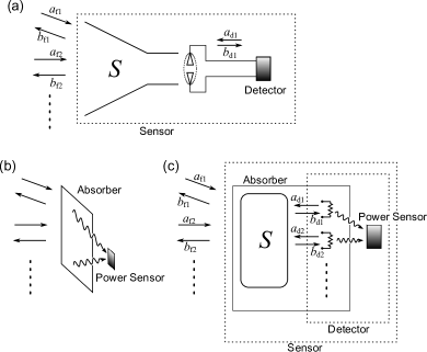
In the context of polarimetry, our focus in evaluating the goodness of a response pattern of a sensor is for control of polarization systematics. In particular, low cross polarization and small differential polarization response are important for high polarization efficiency and low spurious polarization 2003PhRvD..67d3004H; 2008PhRvD..77h3003S, respectively. In this section, we describe the formalism to evaluate the ability of the sensor to reject these artifacts in the angular response and retain the polarization purity of the incident radiation. Throughout this section, the word sensor represents the entire polarimeter including the coupling to the plane wave propagating in free space, while the word detector denotes a part that converts an incoming electromagnetic wave to an electric signal that can be read out (Fig. 2).
It is convenient to discuss the polarization systematics of a multimoded system in contrast to that of a single-mode system, which has already been discussed in detail in literature. We will adopt Ludwig’s third definition 1973ITAP...21..116L, in which the electric field directions of the two linear polarization bases are
| (1) |
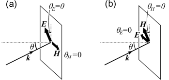
where and are unit vectors in spherical coordinates (see Appendix A). As a convention, we define the axis as the on-axis direction of the optics and take the standard definition of a spherical coordinate system specified by where is the angle from the axis. The vertical (horizontal) polarization direction () asymptotes to the () axis direction for .
It is customary to characterize the beam of a single-mode sensor through the radiation process. Although relevant for a receiver instrument is the reception process, time-reversal symmetry allows us to naïvely relate the characteristics in the radiation process to those in the reception process. For a single-mode sensor nominally sensitive to vertical [horizontal] polarization, the radiation field pattern is described using co- and cross-polar far-field functions, and , as
| (2) |
where is the wave number () and the superscript or (vertical or horizontal) denotes the nominal polarization of the detector. In practical applications, a polarimeter is often a dual-polarization sensor equipped with two detectors nominally measuring two orthogonal polarizations. We refer to such a dual polarization sensor as a single-mode system in the limit each polarization sensitive detector couples a single mode and the polarization isolation can be treated as a subdominant perturbation to the sensor response.
The beam systematics are quantified using the far-field functions. We define the cross-polar level as cross-polar radiation power:
| (3) |
where we indicate the worst case in by . Note that we do not assume normalization of the far-field functions to the on-axis beam and thus the denominator in Eq. (3). The lack of normalization, as opposed to what is often standard, is our intentional choice since it is more appropriate when describing a multimoded system as we see later. The differential response is defined as the difference of co-polar radiation power between the two detectors:
| (4) |
where we again take the worst case in . Zero systematics, i.e., and , are attained when the far-field complex gain response satisfies
| (5) |
We briefly comment on some general properties of the far-field functions and the systematics measures. These properties apply to a scalar feed as well as a multimoded absorber sheet with isotropic resistivity, which we will show later. If the sensor of interest is symmetric under a rotation about the axis, the far-field functions satisfy the following relation:
| (6) |
since the rotational operation acts on the elements in Eq. (2) as and . This justifies the definition of Eq. (3), which may otherwise appear different for . When the coupling to free space possesses continuous rotational symmetry about the axis, the to achieve in Eqs. (3) and (4) corresponds to and , respectively kildal2000foundations. corresponds to the difference of the co-polar beams for the E- and H-planes when this condition is achieved. It is known that a necessary and sufficient condition for a scalar feed to attain zero systematics [satisfy Eq. (5)] is to posses symmetric - and -plane responses, or 1973ITAP...21..116L; kildal2000foundations; stutzman1997atd; 2010ITAP...58.1383Z. The orders of magnitudes of and are typically related as since .
The radiation field pattern is widely used to describe the beam pattern and its systematics for a single-mode system. In contrast, in this paper we mainly discuss reception processes in deriving the beam pattern of a multimoded sensor. This is because a multimoded beam pattern can be represented as a combination of multiple radiation field patterns and the relative excitation strengths among the radiation modes, and the latter is more naturally derived through reception processes. We assume a multimoded sensor with an electrically thin resistive absorber (Fig. 2) lying on the - plane. In the reception process, an incident plane wave induces absorber-surface current () in the () direction. We relate the induced current, , and the amplitude of an incident plane wave, , with an incident angle and a polarization by co- and cross-polar coupling coefficients, and :
| (7) |
where is the absorber surface resistivity in the direction. One would build a dual-polarization sensor by using a stacked pair of resistive grids as the absorber sheet, where each of the grids is aligned in the or direction, and by coupling the thermal signals from and to different power sensors 2011JCAP...07..025K.
Since the system of interest is multimoded, it is implicit in Eq. (7) that the surface current has multiple excitation modes for each of and . The modes may be expressed in terms of two-dimensional Fourier modes of the surface current, and the modal content of the induced current is dependent on , the incident angle and polarization of the plane wave. We will clarify the details of the modal content in the next section. The coefficients represent the couplings between the current and the plane waves regardless of the modal content. When the system of interest is single-moded, the modal content does not depend on and is equated to the far-field functions through the symmetry between the radiation and reception processes. This is not the case for a multimoded system; e.g., the do not describe a radiation field pattern as in Eq. (2). As discussed in the next section, however, we can regard equivalently to the far-field functions for an infinitely large, electrically thin resistive absorber sheet. For example, we show below that one can substitute them into Eqs. (3) and (4) in place of to evaluate the beam systematics.
III Beam Characterization Using the Coupling Coefficients
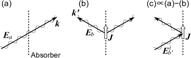
In this section, we derive the relation between the coupling coefficients and the beam characteristics, in particular the beam systematics, for an infinitely large, electrically thin resistive absorber sheet. We first introduce a formalism using a scattering matrix, and relate it to the far-field functions of single-mode and multimoded systems. This allows us to generalize the expressions of the beam pattern, and thus Eqs. (3) and (4), for a multimoded system. We then show in the limit of infinitely large, electrically thin resistive absorbers an incident plane wave with a specific couples to only a single surface-current mode. This simplifies the generalized expressions back to those for a single-mode system, except the far-field functions are replaced by the coupling coefficients . This formalism also shows that our result is applicable to an arbitrary incident mode, even though the definition of Eq. (7) and the drivation in Sec. IV assume plane-wave incident modes. This generalization is of importance since spherical waves are the incident modes when a detector is placed at the focus of a telescope. However, the derivation in Sec. IV does not require this groundwork.
III.1 -Matrix Formalism
A general response of a sensor can be described using a scattering matrix, or matrix, relating the incoming and outgoing modes (see, e.g., Ref. 2003ApOpt..42.4989Z for a formal discussion). Incoming modes are either plane waves from the sky propagating in free space, whose amplitudes are , or radiation from the detector, whose amplitudes are . Outgoing modes, which are the time reversal of the incoming modes, are either plane waves reflected toward the sky with amplitudes , or the modes absorbed by the detector with amplitudes (Fig. 2). The amplitudes are proportional to the electric field strength and follow a Gaussian random distribution for radiation from a thermal source (e.g., the CMB). An matrix describes the coupling of the incoming and outgoing modes provided by an optical coupling element (e.g., a feedhorn) and relates the amplitudes as
| (8) |
where the indices and runs over both and . For simplicity, we omit the dependence on frequency hereafter.
A single-mode sensor measures a single mode among the outgoing modes, which we label as . The -matrix elements relate the incoming plane-wave amplitudes and the measured amplitude :
| (9) |
The detected power is calculated as
| (10) |
where the last equality holds when incoming plane wave amplitudes are uncorrelated to each other. We omit the coefficient, with the dimension of admittance, relating and . Since the index runs over the plane wave modes with different incident angles and polarization, corresponds to the angular and polarization dependent antenna power pattern of the sensor in the reception process.
It is customary to define the far-field functions and in the context of radiation patterns and thus they are related to the -matrix elements for the radiation process, . The system of interest is usually symmetric under time-reversal operation 111Rare exceptions include magnetic devices like circulators. and thus the matrix is Hermitian, . The Hermitian property of the matrix allows us to equivalently relate the far-field functions to the -matrix elements for the reception process, , which are conceptually more straightforward to evaluate for a multimoded system.
A natural extension of Eqs. (9) and (10) describes the response pattern of a multimoded sensor. The formalism differs from a single-mode system in that there are more than one mode coupled to the detector (Fig. 2). The detector-absorbed amplitudes are:
| (11) |
and the detected power is:
| (12) |
where, again, the last equality holds when the incoming plane wave amplitudes are uncorrelated.
The absorbed-mode basis set, with amplitude (), is chosen such that each of the modes couples to an eigenmode of the dissipation process in the device (Fig. 2c). This corresponds to the order of operations in Eq. (12) that the square of the absolute value, , is taken first and then summed over the index . In the subsection III.4 we show that for an infinitely-large, electrically-thin resistive absorber, two-dimensional Fourier modes of the surface currents serves as such eigenmodes.
III.2 Far-Field Functions of Single-Mode Sensors
Here, we relate the matrix to the far-field functions of a single-mode dual-polarization sensor. For convenience, we label the two detectors and indices of the detector-coupled modes by their nominal polarizations, (vertical) and (horizontal), instead of and . Equation (9) is now rewritten as a pair of equations:
| (13) |
Since the index runs over free-space–propagating plane waves, we can choose the basis set such that the label corresponds to a set of an incident angle and a linear polarization . Both matrix and plane-wave amplitudes are relabeled as and , respectively. Equation (13) can be conveniently written in terms of a matrix
| (14) |
with
| (15) |
and . Note that the matrix does not have to be symmetric since it is an off-diagonal block of the entire matrix, which is clear in Eq. (13).
We then equate the matrix to the far-field functions:
| (16) |
As noted earlier, and slightly deviate from the standard definition in that they are not normalized to . Instead, their normalization carries additional information about absorption efficiency.
Now we can rephrase the definitions of the beam systematics in the context of the reception process. The cross-polar level, defined by Eq. (3), is the response in power to a cross-polar incident wave normalized to the response to a co-polar on-axis incident wave. The differential response, defined by Eq. (4), is the difference of the power response between the two detectors to their co-polar incident waves with the same incident angles. This language, in contrast to that of the radiation process, is directly applicable to a multimoded system, too.
III.3 Far-Field Functions of Multimoded Sensors
We relate the matrix to the far-field functions and define the systematics measures for a multimoded dual-polarization sensor by extending those for a single-mode sensor. We relabel the index of the detector-coupled modes, , by a pair , where () labels each of the two detectors and the index runs over the modes coupled to each detector. Hereafter, we use symbols with primes for variables indexing the detector-coupled modes for clearity.
As is done for the derivation of Eq. (14), we rewrite Eq. (11) as:
| (17) |
where and are defined similarly to Eq. (15) but with an additional index . We then define the far-field functions for a multimoded system as a natural extension of Eq. (16):
| (18) |
We note again that the normalizations of the far-field functions here are related to the absorption efficiency; they are not normalized to on-axis response. This is more important here than it is for a single-mode system since the relative normalization among for different tells us the relative excitation strengths among different detector-coupled modes.
We adopt the definitions of the levels of cross polarization and differential response rephrased in the context of reception process using response power:
| (19) |
and
| (20) |
The only difference from a single-mode system is the use of Eqs. (12), (17) and (18), as opposed to Eqs. (10), (14) and (16), in calculating the response powers used in these definitions.
III.4 Simplification for Infinitely Large, Electrically Thin Resistive Absorbers
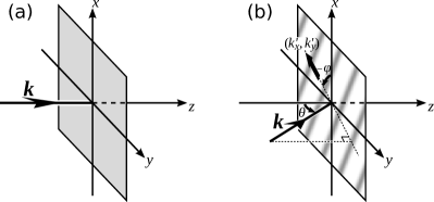
Here, we relate the far-field functions in a multimoded system with the coupling coefficients in Eq. (7) for an infinitely large thin resistive absorber, and show the equivalence between the and the far-field functions for a single-mode system, . The surface current on the absorber sheet is denoted by its two-dimensional Fourier amplitudes, and , where and are the wave numbers of the surface current, and and correspond to current density per unit area of absorber in the and directions, respectively. For later convenience, we identify the Fourier modes using angular variables through and (see Fig. 3); we relabel the current amplitudes as accordingly. We adopt the basis set of detector-coupled modes that maps directly to the Fourier modes of the surface current and use as the index in Eq. (17):
| (21) |
where and are the resistivity of the absorber in the and directions, respectively. We also relabel the matrix, . Recall that we omit possible frequency dependence and thus the discussion here is confined in a single wave number . The detected power for polarization is calculated through Eq. (12) by substituting these definitions:
| (22) |
with and or . We also rewrite Eq. (17) as
| (23) |
We comment on our choice of the basis set of the detector-coupled modes. In order for Eq. (12) to be valid, the basis set has to be the eigenmodes in dissipation process in the device of interest. A trivial choice here is the mode set where each mode couples to spatially localized surface current. Our choice to use the Fourier modes is equivalent to the trivial choice according to Parseval’s theorem (or the unitarity of Fourier transformation).
As shown in Fig. 3 and discussed in Sec. IV, an incoming mode with an incident angle only induces surface currents with a wave vector of . Thus, the matrix can be written in a simplified form as
| (24) |
which is a product of a matrix that is only dependent on , and the angular part of three-dimensional Dirac’s delta function in spherical coordinate system. Equation (23) now reduces to
| (25) |
Substituting Eq. (21) into Eq. (25), we obtain
| (26) |
Comparing Eq. (26) with Eq. (7), one realizes the elements of the matrix are equal to the coupling coefficients previously defined:
| (27) |
The far-field functions are related to the matrix via Eq. (18), where the index in the equation is now labeled by , and thus related to the coupling coefficients through Eqs. (24) and (27) as
| (28) |
As noted earlier, the are not the far-field functions since they do not define a radiation field pattern by Eq. (2). The far-field functions are defined by the left hand side of Eq. (28), where each mode labeled by has a radiation pattern corresponding to a single plane wave, and represents the relative excitation strengths among the modes.
Nevertheless, hold a formal equivalence to the far-field functions in a single-mode system, . For example, substituting Eqs. (25) and (27) into Eq. (22) leads to an expression for the detected power equivalent to that for a single-mode sensor:
| (29) |
with or . Substituting Eq. (28) into Eqs. (19) and (20) yields forms of and that are equivalent to Eqs. (3) and (4)222Note that the label for the detected modes is continuous variable, , in Eq. (28), while it is discrete, , in Eqs. (19) and (20). For a consistent treatment, one should either replace the Dirac’s function in Eq. (28) with Kronecker’s in the substitution, or use Eq. (29) and the literal definitions of and described at the end of Sec. III.2. Both treatments lead to the same result equivalent to Eqs. (3) and (4). . This formal equivalence to a single-mode system allows us to regard in Eq. (7), or in Eq. (28), equivalently to the far-field functions in a single-mode system. Note that Eq. (29) can be generalized to represent the response to an arbritary incoming distribution, which can be expressed as a spectrum of plane waves.
We note that our choice of identifying the Fourier modes by has simplified the derivation above, allowing us to evade possible Jacobians that would arise with an other choice, e.g., . Our choice is convenient since, after relating to through Dirac’s delta function, the power measured by the detector can be calculated through an integral over the solid angle, , as is standard. This has allowed us to directly equate the matrix with the defined in Eq. (7), which are independently introduced; the former is introduced in describing the matrix while the latter is the coupling coefficients in the process where a single plane wave interacts with the sheet absorber and induces the surface current. We also note that the derivation above has clarified the modal content of the current in Eq. (7) and its dependence on the incident angle ; induced current is a pure Fourier mode with a wave vector .
IV Response Pattern of an Infinitely Large, Electrically Thin Resistive Absorber
In this section, we calculate the response patterns for an infinitely large, electrically thin resistive absorber. The absorber sheet may comprise either an electrically thin resistive membrane or a pair of orthogonal grids, where the latter could be constituted as a dual-polarization polarimeter by thermally coupling each of the grids to a power sensor. In the following, we treat the resistive grid-pair absorber equivalently to a membrane absorber regarding its electromagnetic coupling to free space, except that a grid-pair is more general in that it may have different resistivities in the two orthogonal directions. The equivalence is based on the assumptions that the grid is thin and finely pitched, and the distance between the stacked grids is small. Discussions on concrete conditions and the validity of the treatment can be found in Appendix D. Hereafter, we assume the more general case. We define the coordinates such that the absorber sheet is parallel to the - plane, where each absorber grid is aligned in the or direction, and the wave vector of an incoming plane wave is with . Note that, although the calculation in this section assumes a plane-wave incident mode, the discussion in the previous section allows us to apply the calculated result to an arbitrary incident mode through Eq. (29). This is of importance since, in most of uses, the sensor is at the focus of optics, where the mode incident on the sensor is not a plane wave. Appendix E also discusses a case where the incident mode is not a plane wave.
In the following, we first discuss the case of a freestanding thin absorber. Although this is a configuration that minimizes the polarization systematics, the maximum absorption efficiency is limited to 50% as in an analogous case of the transmission line (see also Fig. 13 in Appendix B). We then discuss the case that employs a reflective backshort, which is a technique frequently used to improve the absorption efficiency (see also Fig. 14 in Appendix C). As we will show, it significantly improves the efficiency while introducing small systematics.
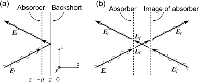
IV.1 Freestanding Electrically Thin Absorber
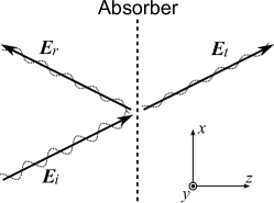
We consider an arrangement shown in Fig. 4, where an electrically thin resistive absorber is at , lying on the - plane. The electric field of an incoming plane wave with arbitrary polarization can be expressed as a linear combination of vertically and holizontally polarized components with amplitudes and :
| (30) |
The transmitted wave () and reflected wave () have wave vectors of and . At , all three plane wave components have the same phase of and only the surface current mode with a wave vector of is induced. Thus, the current density of the induced current is written as
| (31) |
where and are the Fourier amplitudes of the surface current per unit absorber area. In turn, this current only induces radiating electromagnetic waves with the phase of at (Appendix B), and thus the functions in Eq. (24) are confirmed.
Solving boundary conditions (see Appendix B), we derive the coupling coefficients in Eq. (7) relating and :
| (32) |
with
| (33) |
where is the impedance of free space. When the resistivities are the same for the and directions, , the cross-polar level and the differential response defined by Eqs. (3) and (4) are
| (34) |
and
| (35) |
Figure 5 shows and for various .

The most important implication is the case with . As can be seen from Eqs. (32), (33), (26), and (27), this is the necessary and sufficient condition for the matrix relating and to be diagonal,
| (36) |
and for Eq. (5) to be satisfied for . Thus, this surface resistivity achieves zero cross polarization and zero differential response, . We discuss the underlying symmetry that causes the systematics to vanish later in this section.
In this special case of , the angular dependence of the power absorption per unit area of the resistive surface, , is
| (37) |
where represents either or . The power flow of the incident plane wave per unit area per polarization is . Thus, the angular dependence of the absorption efficiency is
| (38) |
where the extra factor of arises in converting the power absorption to be per unit area of incident wave. The efficiency is maximum at 50% at , as expected from an analogous transmission line configuration (see Fig. 13 in Appendix B), and slowly drops as increases since the effective surface resistivity for an off-axis incident wave deviates from . The antenna reception power pattern is obtained by normalizing to its maximum:
| (39) |
where in this case. Figure 6 (top) shows the efficiency and the antenna power pattern . Since is nearly constant, is close to , the naïve expectation due to the geometric factor. By integrating , we obtain the solid angle as a function of the maximum acceptance angle :
| (40) |
Figure 6 (bottom) shows in comparison to the naïve geometric expectation of . For a maximum acceptance at the , while the naïve geometric expectation yields .

It may appear non-trivial that the response of an electrically thin resistive grid or membrane completely eliminates polarization systematics when . One can intuitively understand why the response pattern attains symmetry between the - and -planes (leading to zero systematics) as follows. As shown in Fig. 7, an -plane (-plane) incident wave is a linearly-polarized plane wave with its electric field parallel (perpendicular) to the plane of incidence. When , the - and -plane coupling coefficients, and , relate the amplitudes of the incident field and the induced current as
| (41) |
where () is the electric field amplitude for -plane (-plane) incident since () at . One can see each of Eq. (41) consists of two terms. The first term dominates in the limit (thin film resistor approximates an open) and the second dominates in the limit (termination approximates a short). At the limit of (Fig. 8a), the electromotive force and current-induced field can be ignored. In this limit, the current is simply proportional to the component of the electric field parallel to the resistive surface, and written as
| (42) |
where is the angle between the electric field and the absorber surface. Figure 7 defines such that () for -plane (-plane) incident, and thus Eq. (42) is in agreement with the first terms of Eq. (41).
At the limit of (Fig. 8c), on the other hand, the absorber approximates a perfect electric conductor, and the field of the incident wave and the current are related as , where is the unit vector normal to the absorber sheet. Thus,
| (43) |
where and is the angle between the magnetic field and the absorber sheet surface. For -plane (-plane) incident, () as shown in Fig. 7. When the value of is at neither of the limits, the electric field simply equals to the sum of the voltage drop due to resistivity, Eq. (42), and the electromotive force, Eq. (43); the electric field of the incident wave is related to the current as
| (44) |
This follows from the boundary condition in forming the solution as a linear combination of the limited cases shown in Fig. 8a and 8c. The total incident field is the sum of those for Fig. 8a and 8c: . For this linear combination, the electric field projected on the absorber sheet is simply that of since it vanishes for Fig. 8c. Thus, Ohm’s law corresponds to , where denotes a projection on the plane of the absorber sheet. On the other hand, the field in Fig. 8c satisfies , where is the magnetic field associated to . Substituting these two conditions into leads to Eq. (44).
Equation (44) is equivalent to Eq. (41). Now it is obvious why the current response to the incident wave becomes symmetric between - and -planes when , since this condition makes Eq. (44) symmetric to the exchange of and . This also clarifies the observation and can be used to understand why a wire-grid made from perfect conductor is not a perfect polarizer 2009stt..conf..223L.
It is worth noting that the same angular response as that obtained in the limit of would also show up if we replaced the resistive sheet by a perfect magnetic conductor. In this sense, zero systematics are attained when there are both electric and magnetic conductor sheets and the contributions from the two are equal. This is exactly the same symmetry as the one discussed by Koffman 1966ITAP...14...37K in the context of cross polarization of a feedhorn, where the feedhorn coupled to a paraboloid reflector attains zero cross polarization when the radiation pattern can be described as a balanced sum of electric-dipole and magnetic-dipole radiation fields (Huygens source); see Appendix E for details. The symmetry between the electric and magnetic dipoles discussed by Koffman corresponds to that of electric and magnetic conductor sheets discussed here. We also note that our work can be seen as an extension of the current sheet model for phased-array antennas 1965ITAP...13..506W; hansen2009phased. The model assumes current sheet of surface impedance backed with a magnetic reflector to simulate a phased array, and derives the symmetry of antenna properties, such as the reflection coefficent and scanning impedance, between - and -planes. It parallels to our discussion above and its result is consistent with our derivation. For example, it suggests that the absolute value of the reflection coefficient is in both - and -planes, while Eq. (38) can be rewritten as . The factor two differences both in the absorption efficiency and in the resistivity to achieve the symmetry follow the expectation due to the absence of the magnetic reflector in our setup; see our discussion at the beginning of this section pointing out the analogy to the case of transmission line (cf. Fig. 13 in Appendix B) and the maximum absorption efficiency of 50% without a backshort.
IV.2 Electrically Thin Absorber with Reflective Backshort Termination
Use of a reflective backshort behind the electrically thin absorber sheet improves the absorption efficiency and is desirable in practical applications. We consider an arrangement shown in Fig. 9a, where the absorber is at and a reflective backshort is at , with both parallel to the - plane. In calculating the response pattern, we exploit the image theory and use the arrangement of Fig. 9b.
Solving boundary conditions (see Appendix C), the coupling coefficients are derived as
| (45) |
with
| (46) |
and
| (47) |
This equation is already instructive even without calculating the cross-polar level and the differential response explicitly. In order to eliminate these systematics, the matrix elements should satisfy and . This is only possible if . Even though the first term in vanishes for , cannot be zero for an arbitrary since . Thus, there always are non-zero systematics, unlike the case without a backshort. However, by optimizing the distance to the backshort , a low level of beam systematics can still be achieved.
For , the cross-polar level and the differential response are
| (48) |
| (49) |
Note that Eqs. (48) and (49) are equivalent to the no-backshort case [Eqs. (34) and (35)] only if one substitutes and . Figure 10 shows and for and various . For , a low level of the beam systematics, below dB and below dB, can be achieved for a wide range of acceptance angle, . The and do not significantly degrade for or , suggesting a fractional bandwidth of is possible while maintaining the low levels of systematics.

We define the angular dependence of the power absorption per unit area of the resistive surface, , as an average over :
| (50) |
For one grid running in direction, here is
| (51) |
where the last equality assumes unpolarized incident light with and . When , is
| (52) |
Again, Eq. (52) is equivalent to Eq. (37) if one formally substitutes , except for an overall factor of two. Substituting Eq. (52) into the first equalities of Eqs. (38) and (39), we define the absorption efficiency and the antenna power pattern , respectively. Similarly, we define the solid angle by the first equality of Eq. (40). Figure 11 shows them for various backshort position for . Unlike the case without a backshort, does not always give the maximum ; e.g., when .
In summary, the use of the reflective backshort leads to significant improvement of the absorption efficiency and maintains a large sensor acceptance angle. On the other hand, it also leads to non-zero cross polarization and differential response. However, these systematics can be suppressed for a wide range of incident angles, , by matching resistivity to the free-space impedance and optimizing the backshort position. We also point out that Eq. (46) shows that the differential response (sourced by the term in ) depends on as , yielding an spurious polarization pattern with even parity only and maintaining a systematic-free measurement of the odd-parity patterns 2003PhRvD..67d3004H; 2008PhRvD..77h3003S. This is of importance in the context of CMB polarization observation, where the precision measurement of the so-called -mode, or parity odd, pattern is the primary goal.

In order to see why the beam systematics are small and yet what prevents their exact elimination, we look into the beam patterns in the and planes. For , . When , the coupling coefficients are
| (53) |
We reform them and relate the incident field and the induced current using Eq. (7) as:
| (54) |
where () is the electric-field amplitude for -plane (-plane) incident since .
Equation (54) has an almost equivalent form to the no-backshort case of Eq. (41) except for an extra factor of in the second term; without this factor, the beam pattern is symmetric between and planes when . As we see below, this extra factor can be understood as a reception pattern of a two-element phased-array antenna. Note that the overall phase of in Eq. (54) is physically irrelevant, being due to our convention here that the resistive sheet is placed at , not at .
We again look into the terms in Eq. (54) by considering the limits of (approximately shorted) and (approximately open). Figure 12 illustrates these limits. The first term, which dominates in the limit of , corresponds to a reflection off a perfect conductor sheet (Fig. 12a). In this case, the mirror image in the region has no effect on the sheet located at and thus Eq. (43) describes this component in the same manner as in the case without a backshort (cf. Fig. 8c).
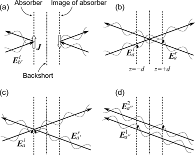
Slightly more complicated are the second terms in Eq. (54), which dominate when . These correspond to the incident field, , and its mirror conjugate, which corresponds to the reflected field , passing through the absorber with negligible interactions (Fig. 12b). It is convenient to decompose into two parts, one of which, called , is phase coherent with at and satisfies (Fig. 12c and d). Then the entire field is represented with two combinations: (c) and ; and (d) a superposition of () and (). Note that has the same phase as by construction, since the image theory forces the field to have a phase shifted by compared to that of . The system with would recover the symmetry between and planes, or the symmetry between Eqs (42) and (43), if there were contributions only from (a) and (c). The relation of the field and current in (c) is the same as that of Eq. (42), except the current here is twice as large since is phase coherent to at :
| (55) |
The contribution from (d) introduces a small violation of the symmetry. This component resembles the reception pattern of a two-element phased-array antenna with uniform (or zero-phase) excitation:
| (56) |
where is the space factor of the phased array. The relation of the current and the incident field in the limit of (Fig. 12b) corresponds to the sum of Eqs. (55) and (56):
| (57) |
where the phase factor arises as a phase difference between (c) and (d); the induced current in (c) is in-phase with at while that in (d) is in-phase with at .
When the surface resistivity is at the neither limits of or , the incident electric field corresponds to the sum of those in Eqs. (43) and (57):
| (58) |
which represents the same boundary condition as that discussed in Fig. 8 for Eq. (44). Equation (58) is equivalent to Eq. (54) obtained from the exact calculation done in Appendix C.
When , the - and -plane responses are maximally symmetric and the residual arises from the phased-array type contribution of Eq. (56). More strictly, the systematics arises due to the difference of this component between and planes; the difference of the coefficient in Eq. (56) is since () for -plane (-plane) incident. This is consistent with the fact that as in Eq. (47).
We close the discussion here by pointing out that a reflective backshort made of perfect magnetic conductor (PMC), as opposed to perfect electric conductor (PEC) or metal, would eliminate the polarization systematics. With the PMC backshort, the ideal configuration of the absorber sheet and the backshort is to place them infinitesimally close to each other. In this case, the phased-array type contribution vanishes and the symmetry between and planes is recovered. Such a configuration is indeed mentioned in the current sheet model as an implementation of an ideal current sheet 1965ITAP...13..506W; hansen2009phased. However, a practical implementation of a PMC tends to have restrictions such as finite bandwidth. This is because an implementation of PMC often consists of a PEC and a quarter wave delay, and the latter introduces a wavelength dependence. Indeed, one can regard the PEC backshort discussed above as a PMC backshort right behind the absorber, where the spatial distance is the quarter wave delay. A phase delay realized by the spatial separation depends both on the incident angle and on the frequency, and only exactly realizes the desired boundary at a single frequency. Thus, it leads to the systematics discussed above in detail.
V Diffraction Effect due to Finite Size of the Absorber
In this section we argue that diffraction effects due to the finite size of the absorber are minor. Such diffraction effects are discussed in detail in Refs. 2003SPIE.4855...49W; 2008PASP..120..430C; Thomas:10. Reference 2008PASP..120..430C shows that the net differential response can be approximated as %, where is the size of the absorber. As expected, the larger is, the smaller the differential response. That analysis also shows that the differential response has a () pattern for a channel sensitive to () polarization. This is significant for the purpose of CMB polarization measurement, as the spurious polarization sourced by this effect does not create the so-called -mode, or parity odd, pattern 2003PhRvD..67d3004H; 2008PhRvD..77h3003S.
The analysis in Ref. 2008PASP..120..430C is for a blackbody absorber or radiator. However, the difference between an electrically thin resistive absorber of interest and a blackbody absorber is minor, and only involves angular response pattern, where the blackbody absorber follows while the absorber sheet follows a different functional shape, Eq. (39), for example. Their difference is small (see, e.g., Fig. 6), and is only significant for large angle incident waves, , which would either be stopped by baffling or have little contribution to the total solid angle. Thus, the diffraction estimate for the blackbody absorber serves as a good order-of-magnitude estimate for an electrically thin resistive absorber, too. A more rigorous estimate of the thin absorber response is possible with the extension presented in Ref. Thomas:10.
We also note that these analyses adopt metal boundary conditions, taking the frame around the absorber as a perfect conductor. Strictly, the diffraction effect depends on the boundary condition and the metal boundary is one of the worst cases. The diffraction pattern in general depends on the impedance of the aperture frame 1996ITAP...44.1464Y.
There are other possible effects that arise due to the finite size of the absorber. For example, the edge of the absorber, which may have different impedance from the main absorbing area, could affect the image quality. Effects of this type are dependent on specific implementations of devices and the configurations in which the devices are placed, such as edge tapering of the absorber resistivity and baffling around the absorber surface. These implementation dependent effects are beyond the scope of this paper.
VI Conclusion
Estimates of polarization beam patterns are presented for a multimoded bolometer employing an electrically thin resistive absorber at the limit of infinitely large area (). For a freestanding thin absorber, cross polarization and differential response can be eliminated by choosing the surface resistivity to be half of the free-space impedance [Eqs. (34) and (35)]. The absorption efficiency can be significantly improved by employing a reflective backshort termination. Although the backshort introduces non-zero cross polarization and differential response, the levels of these systematics can be suppressed by choosing the resistivity matched to the free-space impedance and optimizing the position of the backshort. For a practical application where the absorbing area is finite, diffraction sources additional beam systematics. However, the differential response due to the diffraction is small when the number of modes is large.
The low levels of cross polarization lead to high efficiency in polarization detection. The smallness of the differential response is critical for an accurate measurement of polarization, as it can create spurious polarization from fluctuations in intensity. One significant potential uses for these sensors is to measure the signature of inflation during the early epic of the universe, which manifests itself as odd-parity patterns in the CMB polarization 1997PhRvL..78.2054S; 1997PhRvL..78.2058K. The differential responses due to the two types of residual systematics mentioned above, one due to a backshort and another due to diffraction, have angular patterns of even parity and do not contaminate the inflation signature 2003PhRvD..67d3004H; 2008PhRvD..77h3003S.
Acknowledgment
This work was done in the context of developing experimental projects using multimoded detectors, in particular MuSE and PIXIE. We thank the collaborators of these projects; especially we acknowledge D. J. Fixen, A. J. Kogut, S. S. Meyer, and S. T. Staggs for their insights and persistent encouragement. We thank L. A. Page and N. Jarosik for fruitful discussions. A. K. acknowledges the Dicke Fellowship.
Appendix A Explicit Definitions of Unit Vectors
Unit vectors that define Cartesian coordinates are:
| (59) |
Unit vectors for polar coordinates are:
| (60) |
Here are unit vectors that describe the fields of the two polarization bases in Ludwig’s third definition 1973ITAP...21..116L:
| (61) |
| (62) |
They are perpendicular to by construction and satisfy
| (63) |
Parallel and perpendicular polarization vectors for - plane incident waves are:
| (64) |
They are related to (, ) and (, ) by
| (65) |
where is a rotation matrix around the axis:
| (66) |
Appendix B Analytic calculation of the response of freestanding thin absorber
We consider the arrangement shown in Fig. 4. The electric and magnetic fields of an arbitrary polarized plane wave can be expressed as a linear combination of vertically and holizontally polarized components with amplitudes and :
| (67) |
Amplitudes and are defined for convenience and related to and as
| (68) |
with
| (69) |
The reflected and transmitted fields can similarly be written as
| (70) |
and
| (71) |
respectively, where ; and and are the amplitudes of the transmitted and reflected waves, respectively.
The absorber can either be a membrane or a pair of orthogonal resistive wire grids running in the and directions. For the latter, we allow each grid to have different resistivity, including the case where one of the grids is absent (i.e., infinite resistivity). At , where the absorber is, all three plane wave components have the phase and thus the surface current density on the absorber induced by the incident field can be written as
| (72) |
where and are complex current amplitudes.
The vector potential of the field induced by the current is the solution of the following Helmholtz equation:
| (73) |
with magnetic permeability . Note that we implicitly choose the Lorenz gauge by adopting the Helmholtz equation. The solution is
| (74) |
and the corresponding electric and magnetic fields () are
| (75) |
Thus, the field discontinuity at due to the current is
| (76) |
where is the wave impedance the surrounding medium (e.g., vacuum). The electric and magnetic fields of the left hand side are related to Eqs. (67), (70), and (71) evaluated at . This leads to the following boundary conditions on the field amplitudes:
| (77) |
and
| (78) |
where the former [latter] comes from the electric [magnetic] field component of Eq. (76).
In addition to the Maxwell equations used above, the current density and the electric fields at are related by Ohm’s law, leading to
| (79) |
where and are the surface resistivities of the absorber in the and directions, respectively.
Solving Eqs. (77), (78) and (79), we obtain
| (80) |
| (81) |
| (82) |
where , , and are transmission, reflection, and absorption matrices defined as
| (83) |
| (84) |
| (85) |
with
| (86) |
Combining Eqs. (68) and (82), we obtain
| (87) |
where
| (88) |
with
| (89) |
When the matrix is diagonal, the vertical (horizontal) polarization amplitude () only couples to the () current amplitude () and thus cross polarization is zero. Further, when the two diagonal elements of are equal, the angular response patterns to vertical and horizontal polarization waves are the same and thus the differential response is zero.
For on-axis incidence with , the relation between the incident field and the current is equivalent to the case for a one-dimensional transmission line (Fig. 13), as expected:
| (90) |
Appendix C Analytic calculation of the response of thin absorber with reflective backshort termination
We adopt image theory and use the setup of Fig. 9b. As the mirror conjugate flips the sign of the components of vectors and the sign of the electric field, the conjugate field of can be written as
| (91) |
with
| (92) |
The conjugates of the reflected and transmitted components, and , respectively, and all the associated magnetic fields can be defined in the same way. In particular, those for the transmitted field are
| (93) |
The boundary condition is defined in the same manner as Eq. (76) but at the surface of , leading to
| (94) |
and
| (95) |
with . On the other hand, Ohm’s law leads to
| (96) |
Solving Eqs. (94), (95) and (96), we obtain
| (97) |
with
| (98) |
Combining this with Eq. (68), we obtain
| (99) |
where
| (100) |
with
| (101) |
and
| (102) |
Again, for on-axis incidence, , the relation between the incident field and the current is equivalent to that of the one-dimensional transmission line (Fig. 14), as expected:
| (103) |
with
| (104) |
Appendix D Possible Systematics due to the Finite Physical Size of the Grids
All the discussions in this paper are based on an assumption that the absorber can be modeled as a thin resistive membrane. When the absorber is a pair of orthogonal grids, it deviates from the ideal membrane model in the following three ways: 1) there is a finite distance between the layers of orthogonal grids, 2) the grids have non-zero pitch and consist of wires with non-zero cross-sections, and 3) the two orthogonal grids may couple to each other through near-field effects. In this Appendix, we estimate the magnitude of the systematics due to these aspects and discuss the conditions on the physical dimensions of the device required to suppress such artifacts.
D.1 Non-zero Distance between the Two Layers
When the absorber is a pair of resistive grids, which are sensitive to orthogonal polarizations, there is a finite gap between the two grid layers. This may lead to additional beam systematics of cross polarization and differential response. To estimate the effect, we consider a freestanding absorber with , where there is no systematics in the nominal configuration.
We first point out that the primary effect here is the cross polarization, not the differential response. This can be seen in Eq. (32); when , the response of the grid running in the direction, , is independent of including the case where the grid running in the direction is absent, or . Thus, the co-polar beam shape does not see the effect of the other grid to first order.
Cross-polarization, on the other hand, can arise from the finite gap. Consider the electric fields of incident, reflected, and transmitted waves projected on the absorber surface plane (- plane), , , and , respectively, for vertical polarization incident. Figure 15a shows an example with an incident angle of , where the cross polarization is maximum, and . The boundary condition guarantees . Zero cross-polarization of the nominal configuration corresponds to a vanishing component of the field: . However, this cancellation of the components of the incident and reflected fields is only exact on the surface of the grid running in the direction, which we define as . When the other grid running in direction is placed at (Fig. 15b), the grid feels a residual electric field of order
| (105) |
Thus, the cross-polar level is
| (106) |
D.2 Finite Pitch and Cross Section of the Grid
Compared to an ideal resistive sheet, a grid of resistive wires has non-zero spacing between the grid wires and non-zero cross section of each wire. These can cause deviations from the ideal current sheet when the physical dimensions are not small compared to the wavelength . The requirements for the smallness are discussed in detail in literature (see, e.g., Refs. 1962ITMTT..10..191L; 2012ApOpt..51..197C and references therein) in the context of grids made of conductive wires. Estimates for the grid of resistive strips do not significantly deviate from conductive wires when the resistivity is similar to or less than the impedance of free space, 1987ITAP...35.1492G; Zinenko1998, which is the parameter space of interest here. In the regime , where is the spacing between the wires and is the radius of each wire of circular cross-section, the first order estimates of the cross-polar level and the differential response are (see, e.g., Ref. 1962ITMTT..10..191L)
| (107) |
An estimate for a grid made of thin strips of width can be obtained by substituting , to first order. In the regime , the approximation of the term involving becomes invalid as pointed out in Ref. 2012ApOpt..51..197C. However, the numerical analysis in the reference shows that the term is still a monotonically decreasing function of . Thus, one can still put a rough upper limit on the systematics based on Eq. (107) and the monotonic dependence on even in this regime. In the implementation of Ref. 2011JCAP...07..025K, for example, the parameters are and , and satisfy . The systematics in this case are and , negligibly small for millimeter and submillimeter wavelengths.
D.3 Near-field Coupling
All the discussions above assume only the far-field effects, or the radiating modes, and we ignored the near-field effects due to the evanescent modes. Here we show that the near-field coupling between the orthogonal grids is small when the distance between the grids, , is similar to or larger than the grid spacing, . Owing to the periodic symmetry of the system, the scattered field including the evanescent modes can be expanded in terms of a Floquet series Zinenko1998; Matsushima2000. The phase component of the Floquet series is
| (108) |
with
| (109) |
where is the distance from the scattering grid, and and are the integer numbers corresponding to the series indices. Our interest here is the non-radiating modes, or the modes with or . When the grid spacing is small compared to the wavelength (), the non-radiating mode has
| (110) |
and the field strength decays as or faster. Thus, the near-field coupling between the paired grids is suppressed by a factor of . This factor is small when is similar to or larger than the grid pitch (). Therefore, the near-field effect can safely be ignored in this regime of , with .
Appendix E Relation among Resistive Sheet, Conic Reflector, and Parallel Current on Their Surface
Koffman showed the condition where the induced current on a conic reflector illuminated by a feed flows in parallel 1966ITAP...14...37K. The condition is met when the magnetic field at the reflector surface satisfies
| (111) |
where the angle specifies a position on the reflector with the focus as the origin of the coordinates, and are the magnetic field along and , respectively, and is the eccentricity specifying the geometry of the conic reflector: , , , , and correspond to sphere, ellipsoid, paraboloid, hyperboloid, and plane, respectively. Koffman pointed out that a feed radiation pattern satisfies Eq. (111) when it can be expressed as a superposition of electric- and magnetic-dipole radiations, and relative strengths between them coincide with the eccentricity . Note that the object is at infinitely far for astronomical applications and thus a paraboloid reflector or an equivalent system Mizuguchi; Dragone is usually employed. This is why we adopted Ludwig’s third definition, in which a pure polarization pattern satisfies Eq. (111) with .
We can see two connections between this symmetry explored by Koffman and our result for a freestanding resistive absorber sheet. One of them can be seen by replacing the feed in Koffman’s setup by a resistive sheet. In the replacement, we also replace the radiation field pattern from a pure-polarization feed by the absorption field pattern that induces current in only , i.e., . Equations (65), (67), and (68) lead to . Thus, Eqs. (87), (88), (89), and lead to
| (112) |
for the reception pattern of the thin resistive absorber. Equations (111) and (112) have equivalent form, due to the following parallel between Koffman’s and our results: () corresponds to magnetic dipole (magnetic conductor sheet), while () corresponds to electric dipole (electric conductor sheet); the electric and magnetic contributions balances when (). See also the discussion at the end of Sec. IV.1.
Another connection between Koffman’s and our results can be seen by replacing the conic reflector in Koffman’s setup with a freestanding thin resistive absorber. Namely, one illuminates the resistive absorber by a superimposed electric- and magnetic-dipole radiations with their relative strength of . According to the derivation above, the induced current on the absorber flows in parallel when the sheet resistivity satisfies . Thus, instead of the eccentricity of the conic reflector, one can use the resistivity of the absorbing sheet as the parameter tuned to match with an arbitrary superposition of the dipoles.