Thermal and Thermoelectric Properties of Graphene
Abstract
The subject of thermal transport at the mesoscopic scale and in low-dimensional systems is interesting for both fundamental research and practical applications. As the first example of truly two-dimensional materials, graphene has exceptionally high thermal conductivity, and thus provides an ideal platform for the research. Here we review recent studies on thermal and thermoelectric properties of graphene, with an emphasis on experimental progresses. A general physical picture based on the Landauer transport formalism is introduced to understand underlying mechanisms. We show that the superior thermal conductivity of graphene is contributed not only by large ballistic thermal conductance but also by very long phonon mean free path (MFP). The long phonon MFP, explained by the low-dimensional nature and high sample purity of graphene, results in important isotope effects and size effects on thermal conduction. In terms of various scattering mechanisms in graphene, several approaches are suggested to control thermal conductivity. Among them, introducing rough boundaries and weakly-coupled interfaces are promising ways to suppress thermal conduction effectively. We also discuss the Seebeck effect of graphene. Graphene itself might not be a good thermoelectric material. However, the concepts developed by graphene research might be applied to improve thermoelectric performance of other materials.
I Introduction
The Nobel Prize in Physics in 2010 was awarded to Andre Geim and Konstantin Novoselov for their groundbreaking experiments regarding graphene. Graphene is a monolayer of carbon atoms arranged in a regular hexagonal lattice, representing the thinnest material that nature can provide. The research interest of graphene has been growing explosively in the recent years,Geim-07NM ; Castro-09RMP ; Sarma-11RMP ; Balandin-11NM as graphene is of great importance to both fundamental research and practical applications. Graphene is the first truly two-dimensional (2D) material and provide an ideal playground to study low-dimensional physics. Meanwhile the existence of massless Dirac Fermions in graphene enables a new paradigm of “relativistic” condensed-matter physics.Geim-07NM ; Castro-09RMP ; Sarma-11RMP This unique material supports exceptional properties that are useful for optics, electronics, magnetics, etc.Geim-07NM ; Castro-09RMP ; Sarma-11RMP ; Balandin-11NM
Early-stage graphene research intensively focused on electronic properties.Geim-07NM ; Castro-09RMP ; Sarma-11RMP In comparison, the study of thermal properties begins later, but soon becomes an active fieldBalandin-11NM ; Balandin-10FNCN ; Balandin-11AME ; Nika-12JPCM ; Sadeghi-12SSC ; Pop-12MRSB ; Balandin-12MT ; Shahil-12SSC ; ShiL-12NMTE after the first measurements of thermal conductivity of graphene by Balandin et al. in 2008.Balandin-08NaL Graphene offers new opportunities to the development of thermal and thermoelectrics. Unusual thermal transport phenomena and physics emerge in this unique 2D system. Graphene has been experimentally shown to have superior thermal conductivity.Balandin-11NM Furthermore, previous theoretical works predict that thermal conductivity gets divergent with increasing transport length in low-dimensional systems.lepri03pr ; basile06prl ; casher71jmp ; lippi00jsp ; dhar01prl ; yang02prl ; narayan02prl ; saito10prl In this context, it becomes fundamentally important to study the size-dependent behaviors and to find key factors that drive ballistic-diffusive transition. Moreover, it is known that quantum effects become more important in low-dimensional systems than three-dimensional (3D) systems. The 2D graphene sheet or quasi one-dimensional (1D) graphene nanoribbons (GNRs)HuangB-09FPC ; BaiJW-10MSER ; lan2009edge ; jiang2010isotopic ; LiZY-08PRL ; LiZY-10JNN may support prominent quantum effects in thermal transport, like weak localization caused by quantum interference. Last, but not least, the low dimension of graphene systems could significantly affect the scattering strength of various scattering processes,nika09prb ; xu2014 leading to unusual thermal transport behaviors. All these are issues of fundamental importance. The corresponding research could help us to find approaches to effectively control thermal conduction. As applications, thermal conduction of materials can be improved for solving the serious heat dissipation and breakdown in ever-smaller electronic devices,Pop-06PIEEE ; Pop-10NaR ; PangL-10JEM ; PangL-12JPD ; PangL-12TED ; LiaoA-10PRB ; Tsai-11APL or suppressed for realizing thermal insulation in high-power engines and also for enhanced thermoelectric efficiency.Dresselhaus-07AM ; Snyder-08NM
We review thermal and thermoelectric properties of graphene, motivated by the exotic low-dimensional phenomena and physics as well as the great potential for applications.Subrina-09EDL ; YanZ-12NC ; Shahil-12NaL ; Goyal-12APL ; Goli-14JPS We will summarize the most recent experimental progresses, provide a general physical picture on underlying mechanisms, and further suggest possible ways to tune thermal and thermoelectric properties of graphene as well as other materials.
II Basics of Thermal Transport
Various theoretical approaches have been used to study thermal transport in graphene, including molecular dynamics (MD),evans2010thermal ; OngZY-11PRB ; HuJN-11APL ; yang12apl ; zhang2011thermal Boltzmann transport equation (BTE),nika09prb ; Lindsay-10PRB2 ; Lindsay-10PRB3 ; Lindsay-11PRB ; Aksamija-11APL ; Aksamija-12PRB non-equilibrium Green’s function (NEGF),XuY-09APL ; XuY-10PRB ; jiang11apl ; lu12apl ; yang12apl ; Serov-13APL and Landauer approach.Saito-07PRB ; XuY-09APL ; XuY-10PRB Herein we mainly introduce the Landauer approach, which is a widely used theoretical tool for mesoscopic transport.Datta97 The approach can be generally applied to investigate ballistic-diffusive transport for systems from 1D to 3D.XuY-08PRB Importantly, it is conceptually simple, which enables us to build a clear and general physical picture to understand rich thermal transport phenomena in graphene.
In the Landauer transport formalism, the lattice thermal conductance is written as
| (1) |
where is the Boltzmann constant, is the absolute temperature, is the Planck constant, , is the reduced Planck constant, is the phonon frequency, is the phonon transmission function.XuY-10PRB . The distribution of phonon modes counts the number of phonon transport channels at a given frequency , which is equal to the ballistic phonon transmission function. The transmission probability is equal to 1 in the ballistic limit and in the diffusive limit, where is the phonon mean free path (MFP) for backscattering. When quantum interference effects are neglected, we get a quasi-classical formula
| (2) |
where is the transport length.XuY-08PRB The formula, which is exact in both ballistic and diffusive limits, can be used to describe the ballistic-diffusive transport.XuY-10PRB It is interesting that the Landauer formula reproduces the BTE in the diffusive limit.XuY-08PRB ; jeong10jap However, one should notice that the MFPs used in the BTE and in the Landauer approach are not exactly the same. The BTE uses a common MFP defined as the average transport distance between two successive scatterings. While the Landauer approach uses the MFP for backscattering, since in the Landauer approach transport quantities are determined by transmission, to which only backscattering is related. If assuming isotropic phonon bands, the ratio of backscattering MFP to common MFP is , and for 1D, 2D and 3D systems, respectively.jeong10jap Without specification, we will use to denote the MFP for backscattering, which is the MFP relevant to transport in the Landauer framework.
By assuming in Equation (1), we get . , called as thermal conductance quantum, represents the maximum possible value of energy transported per conduction mode. In contrast to electrical conductance quantum, thermal conductance quantum is not a constant but proportional to temperature. The existence of the quantum of thermal conductance was theoretically predicted in 1998 Rego-98PRL and experimentally proved in 2000.Schwab-00N Equation (1) shows that thermal conductance is a weighted integration of phonon transmission function. The weighting factor, , plays an essential role in determining thermal conduction contribution. The factor is equal to one at , decreases quickly with increasing , and becomes vanishingly small when . This tells us that thermal conduction are mainly contributed by low frequency phonons, and phonons with frequency higher than have negligible contribution to thermal conduction.
In theoretical calculations, is determined from phonon dispersion by counting transport channels. The ballistic thermal conductance as a function of temperature is then obtained from Equation (1). Thermal transport studies usually use the approximation of constant phonon MFP (), which does not rely on any assumption about the possible dependence on temperature of the phonon MFP. In this approximation, and are related by , which gives in the diffusive limit (). The lattice thermal conductivity is defined as , where is the cross-sectional area. The diffusive is thus given byxu2014 ; Bae-13NC
| (3) |
This is a very useful relation. As is easily obtained by theoretical calculations and the diffusive is measured by experiments, the combined information from theory and experiment determines , one of the most important length scales in thermal transport. Based on the estimated , we know that thermal transport is ballistic if , or diffusive if , or in the intermediate region otherwise.
Thermal conduction in graphene is mainly contributed by lattice vibrations (i.e., phonons), and the contribution of electrons is expected to be negligible according to theoretical calculationsSaito-07PRB ; Watanabe-09PRB . Indeed, very recent experimentsFong-13PRX ; Yigen-13PRB ; Yigen-14NaL showed electron thermal conductivity is much less than total thermal conductivity ( 1%) in suspended graphene. We thus focus on discussing the lattice vibration contributed thermal conduction. Hereafter, without specification we simply use and without the subscript “” to denote thermal conductance and thermal conductivity of lattice vibrations.
III Experimental Methods
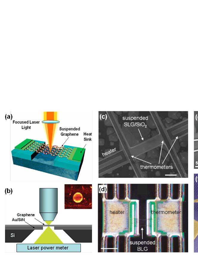
Measuring nanoscale thermal transport is quite challenging due to high requirements of sample fabrication and temperature sensing.Cahill-12JHT ; Brites-12NaS So far, methods used to probe thermal conduction in graphene include optothermal Raman thermometry,Balandin-08NaL ; Ghosh-08APL ; Ghosh-09NJP ; Ghosh-10NM ; CaiWW-10NaL ; LeeJU-11PRB ; ChenSS-11ACSN ; ChenSS-12NM ; ChenSS-12NaT ; Faugeras-10ACSN ; Vlassiouk-11NaT ; Ermakov-13NaT thermoreflectance technique,Mak-10APL ; Koh-10NaL ; Hopkins-12NaL ; ZhangCW-13Carbon 3 method,ChenZ-09APL micro-resistance thermometry,Seol-10S ; Seol-10JHT ; WangZQ-11NaL ; Sadeghi-13PNAS ; Pettes-11NaL ; WangZQ-11NaL ; Jang-10NaL ; Bae-13NC ; Jang-13APL electrical self-heating method,Dorgan-13NaL ; XieHQ-13APL and scanning thermal microscopy (SThM).Yu-11APL ; Pumarol-12NaL ; Menges-13PRL Here we mainly discuss and compare two techniques widely used to measure in-plane thermal conductivity of graphene, i.e., optothermal Raman thermometry and micro-resistance thermometry.
The optothermal Raman thermometry technique was developed by Balandin et al.Balandin-08NaL to measure suspended, micrometer scale (m) graphene. A laser light was focused at the center of the suspended graphene flake to generate a heating power and raise temperature locally (Figure 1a and 1b). Meanwhile, the Raman spectrum of graphene was recorded and the temperature rise could be monitored by calibrating it with Raman G peak position,Balandin-08NaL ; Ghosh-08APL ; Ghosh-09NJP ; Ghosh-10NM ; CaiWW-10NaL 2D peak positionLeeJU-11PRB ; ChenSS-11ACSN ; ChenSS-12NM ; ChenSS-12NaT (only for monolayer), or Stokes/anti-Stokes ratio.Faugeras-10ACSN ; Vlassiouk-11NaT By knowing the correlation between and , as well as the geometry size of suspended graphene, its in-plane thermal conductivity can be extracted through the solution of the heat diffusion equation. The early experimentsBalandin-08NaL ; Ghosh-08APL ; Ghosh-09NJP ; Ghosh-10NM were carried out on graphene strips suspended over a trench (Figure 1a). This was modified in subsequent experimentsCaiWW-10NaL ; Faugeras-10ACSN ; LeeJU-11PRB ; ChenSS-11ACSN ; ChenSS-12NM ; ChenSS-12NaT by adopting circular holes with graphene over them (Figure 1b), which matches with the radial symmetry of the laser spot and allowed for an analytic solution of the temperature distribution.Sadeghi-12SSC
A major source of uncertainty in different works using the Raman thermometry technique is determining the laser power absorbed by graphene, that is, determining optical absorbance of graphene. Balandin et al.Balandin-08NaL and Ghosh et al.Ghosh-08APL ; Ghosh-09NJP ; Ghosh-10NM evaluated this number by comparing the integrated Raman G peak intensity of graphene with that of highly oriented pyrolytic graphite (HOPG), leading to 9% if converted to optical absorbance for exfoliated single-layer graphene (SLG).Sadeghi-12SSC The measured value of 9% considered two passes of light (down and reflected back) and resonance absorption effects due to close proximity of graphene to the substrate, and corresponded to 488-nm wavelength where absorption is higher than the 2.3% long-wavelength limit.Nair-08S Faugeras et al.,Faugeras-10ACSN Lee et al.,LeeJU-11PRB and Vlassiouk et al.Vlassiouk-11NaT did not measure the optical absorbance under the conditions of their experiments and assumed a value of 2.3% for exfoliated SLG based on a separate optical transmission measurement.Nair-08S Cai et al.CaiWW-10NaL and Chen et al.ChenSS-11ACSN obtained values of 3.31.1% and 3.40.7% for CVD SLG by directly measuring the optical transmittance via addition of a power meter under the suspended portion of graphene (Figure 1b). The used optical absorbance is very important because it would proportionally change extracted . We note that both theoryYangL-09PRL and experimentsKimKS-09N ; Kravets-10PRB ; Mak-11PRL showed an increase of optical absorbance in graphene with decreasing laser wavelength due to many-body effect, and the values of Cai et al.CaiWW-10NaL and Chen et al.ChenSS-11ACSN are consistent with those experimental results. To obtain reliable , it is thus necessary to measure optical absorbance under used laser wavelength and specific experimental conditions.
Another uncertainty source is the calibration of temperature with features of Raman spectrum. It is known that strains and impurities in graphene can affect the Raman peak positions and their temperature dependence,Ferrari-11NN which greatly limits the temperature sensitivity of the Raman thermometry technique. In addition, heat loss from graphene to the surrounding air was neglected in most experiments, but Chen et al.ChenSS-11ACSN found that for a large diameter (9.7 m) graphene flake, the obtained in air could be overestimated by 1440% compared with the value obtained in vacuum. This implies measurable errors in previous experiments, even though the influence might be weaker due to smaller sizes of measured graphene. Furthermore, extra uncertainty could come from the difference in between suspended and supported portions of graphene, as well as thermal boundary resistance between graphene and supporting substrates.CaiWW-10NaL Overall, the Raman thermometry technique provides an efficient way to measure of suspended graphene with benefits of relatively easy sample fabrication, reduced graphene contamination, and simple data analysis, but it inevitably has limitations: (i) relatively large uncertainty (up to 40%);Balandin-11NM (ii) difficulty to probe the low temperature regime due to significant heating in graphene by laser; (iii) inability to be applied to nanometer scale or supported graphene, where edge and interface will take effect.
The micro-resistance thermometry technique is a steady-state method to directly probe heat flows in materials.Cahill-12JHT It is able to measure both suspended and supported graphene, as well as at the nanometer scale and in low temperature range, with high resolution of temperature by employing electrical resistance as thermometers. This technique can be further divided into two kinds: suspended bridge platform and fully substrate-supported platform. The former was first developed by Shi et al.ShiL-03JHT ; Moore-11MST to measure thermal conductivity of 1D nanostructures, and it has been widely used for nanotubesKim-01PRL ; YuC-05NaL ; ChangCW-06PRL ; ChangCW-08PRL ; Pettes-09AFM ; YangJK-11Small and nanowires.LiDY-03APL ; Hochbaum-08N ; Boukai-08N ; ChenRK-08PRL ; Lim-12NaL By using this platform, graphene can be either supported by a suspended SiO2/SiNx membrane connecting two thermometersSeol-10S ; Seol-10JHT ; WangZQ-11NaL ; Sadeghi-13PNAS (Figure 1c) or fully suspended over two thermometer padsPettes-11NaL ; WangZQ-11NaL (Figure 1d), enabling measurements of both suspended and supported graphene. The fully substrate-supported platform was developed by Jang et al.Jang-10NaL and Bae et al.,Bae-13NC where at least two thermometers were patterned on Si/SiO2-supported graphene (Figure 1e) or GNRs (Figure 1f). In both platforms, one thermometer serves as the heater to generate heating power and a temperature gradient across graphene by electrical heating, meanwhile all thermometers (including the heater) monitor temperature changes in terms of their electrical resistance changes. Then, the thermal conductance/conductivity of measured materials can be extracted in a simple analytic way by solving its equivalent thermal resistance circuit for the suspended bridge platform,ShiL-03JHT ; Moore-11MST while a complicated 3D numerical (finite element) simulation has to be performed for the substrate-supported platform due to significant heat leakage into the substrate.Jang-10NaL ; Bae-13NC
Although the data extraction of the suspended bridge platform is easier than that of the substrate-supported platform, as a trade-off the sample fabrication is more complicated for the former than the latter. Thus, for materials which are hard to be suspended, such as GNRs, the latter is an advantageous method to be employed. However, the measurable length of interested materials cannot be longer than a few micrometer for the substrate-supported platform, because the temperature drops nearly exponentially away from the heater, leading to undetectable if other thermometers are far away. It is worth noting that for the platform of graphene supported by a suspended membrane (Figure 1c) and the substrate-supported platform (Figure 1e and 1f), a control experiment has to be carried out by etching off graphene/GNRs and repeating measurements to calibrate the background heat flow and thermal contact resistance between graphene and thermometers.Seol-10S ; Seol-10JHT ; Jang-10NaL ; Bae-13NC This improves the measurement accuracy. Whereas, for the platform of graphene fully suspended (Figure 1d) such a control experiment cannot be performed, so the thermal contact resistance could be a main source of uncertainty in results. Overall, the micro-resistance thermometry technique has very high resolution of temperature ( 50 mK)Balandin-11NM ; Sadeghi-12SSC and can cover a wide temperature range. It can probe both suspended and supported graphene, as well as in nanometer scale. However, attention should be paid to micro/nanofabrication, which could introduce contaminations (like residues and defects) and increase the uncertainty.Pettes-11NaL
IV Intrinsic Thermal Conductivity of Graphene
In this section, we mainly discuss the “intrinsic” thermal conductivity of SLG based on experimental results and theoretical analysis. Here, by “intrinsic” we mean isolated, large scale, pristine graphene without suffering impurity, defect, interface, and edge scatterings, so its thermal conductivity is only limited by intrinsic phonon-phonon scattering due to crystal anharmonicityBalandin-11NM and electron-phonon scattering. In experiments, suspended, micrometer scale graphene samples have properties close to intrinsic ones. We thus first summarize current experimental observations of in suspended SLG, then discuss the underlying physical origins of high thermal conductivity in graphene.
IV.1 Experimental Results
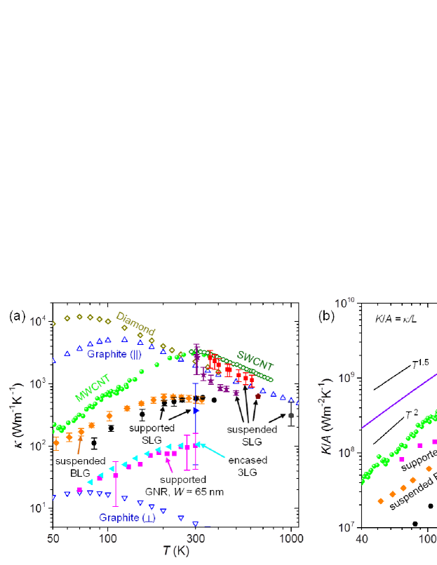
Using the Raman thermometry technique described above, suspended micro-scale graphene flakes obtained by both exfoliation from graphiteBalandin-08NaL ; Ghosh-08APL ; Ghosh-09NJP ; Ghosh-10NM ; LeeJU-11PRB ; Faugeras-10ACSN and CVD growthCaiWW-10NaL ; ChenSS-11ACSN ; ChenSS-12NM ; ChenSS-12NaT ; Vlassiouk-11NaT have been measured at room temperature and above. Some representative data versus temperature from these studies are shown in Figure 2a. The obtained in-plane thermal conductivity values of suspended SLG generally fall in the range of 2000-4000 Wm-1K-1 at room temperature, and decrease with increasing temperature, reaching about 700-1500 Wm-1K-1 at 500 K. The variation of obtained values could be attributed to different choices of graphene optical absorbance (see Section III), thermal contact resistance, different sample geometries, sizes, and qualities. For comparison, we also plot the experimental thermal conductivity of diamond,Ho-72JPCRD graphite,Ho-72JPCRD and carbon nanotubes (CNTs)Kim-01PRL ; Pop-06NaL in Figure 2a. It is clear that suspended graphene has thermal conductivity as high as these carbon allotropes near room temperature, even higher than its 3D counterpart, graphite, whose highest record of observed in-plane in HOPG is 2000 Wm-1K-1 at 300 K. The presently available data of graphene based on the Raman thermometry technique only cover the temperature range of 300-600 K, except one at 660 K reported by Faugeras et al.Faugeras-10ACSN showing 630 Wm-1K-1. For higher temperature, Dorgan et al.Dorgan-13NaL used the electrical breakdown method for thermal conductivity measurements and found 310 Wm-1K-1 at 1000 K for suspended SLG. The overall trend of present graphene data from 300 K to 1000 K shows a steeper temperature dependence than graphite (see Figure 2a), consistent with the extrapolation of thermal conductivity by Dorgan et al.Dorgan-13NaL This behavior could be attributed to stronger second-order three-phonon scattering () in graphene than graphite enabled by the flexural (ZA) phonons of suspended graphene,Nika-12NaL similar to the observations in CNTs.Mingo-05NaL ; Pop-06NaL For temperature below 300 K, the micro-resistance thermometry technique needs to be employed for measurements. Unfortunately, there is no reliable data for suspended single-layer graphene until now. However, data do exist for suspended few-layer graphene (FLG),Pettes-11NaL ; WangZQ-11NaL ; Jang-13APL which will be discussed in Section V.5. It is instructive to compare experimental results with the ballistic limit of graphene as a check, so we convert measured in Figure 2a to thermal conductance per unit cross-sectional area, , which are re-plotted in Figure 2b with graphene (discussed in the next section). Above room temperature, measured of suspended SLG are more than one order of magnitude lower than , indicating the diffusive regime. The reason that the value of Faugeras et al.Faugeras-10ACSN is much lower than others is because of a much larger m (radius) of their suspended graphene.
IV.2 Ballistic Thermal Conductance
Graphene has been demonstrated experimentally to possess very high thermal conductivity.Balandin-11NM ; Nika-12JPCM ; Sadeghi-12SSC ; Pop-12MRSB What distinguishes graphene from conventional materials in thermal conduction? What is the underlying mechanism to the superior thermal transport ability of graphene?
According to Equation (3), two mechanisms could induce high : (i) large ballistic thermal conductance per unit area and (ii) long phonon MFP . It is crucial to distinguish the two possibilities, which lead to essentially different strategies to tune thermal conduction in graphene. If graphene has a superiorly large , would keep large in small samples. While, if of graphene is extraordinarily long, would exhibit a strong size dependence, and thermal transport in small samples is ballistic or quasi-ballistic, accompanied by a small that can be enhanced by increasing . In this context, it becomes important to calculate ballistic thermal conductance.
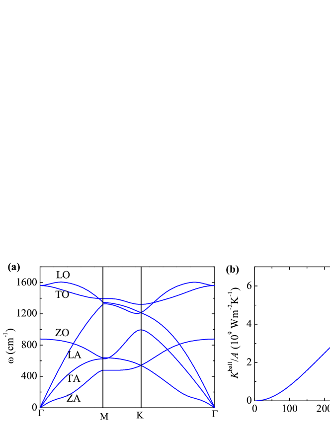
Let us first look at the phonon dispersion of graphene (see Figure 3a), which was discussed previously, for instance, in Refs. Nika-11PSSB, ; Cocemasov-13PRB, . Graphene has two carbon atoms in a unit cell, resulting in six phonon bands: three acoustic and three optical bands. These include in-plane transverse acoustic (TA) and optical (TO) modes, in-plane longitudinal acoustic (LA) and optical (LO) modes, and out-of-plane acoustic (ZA) and optical (ZO) modes. For graphene, phonon bands are very dispersive, and the maximal phonon frequency is about 1600 cm-1, which is quite high compared to other materials (e.g., 500 cm-1 in siliconyu99fundamentals ). These features, explained by the strong bonds and the light atomic mass of graphene, are favorable for thermal conduction.
The ballistic thermal conductance of graphene has been discussed previously based on empirical force field.Mingo-05PRL ; Saito-07PRB ; Bae-13NC Here we combine density function theory and Landauer approach to calculate of graphene as a function of temperature, getting results consistent with previous work.Mingo-05PRL ; Saito-07PRB ; Bae-13NC Herein , where is the width, and nm is the the effective thickness selected as the layer separation in graphite. As shown in Figure 3b, is zero at K and increases monotonically with temperature. It is as large as Wm-2K-1 at K. The same value has been obtained for GNRs with zigzag edges.XuY-09APL
At this point, it is worthwhile to compare between graphene and other materials. The room-temperature is around 1.0 Wm-2K-1 in silicon,jeong11jap smaller than that of graphene but on the same order. It decreases one order of magnitude in Bi2Te3 to around 1.0 Wm-2K-1.jeong11jap Moreover, we compute the ballistic thermal conductance for a newly found 2D topological insulator material, fluorinated stanene (Sn-F), which is a monolayer tin (Sn) film in a honeycomb lattice decorated by fluorine.XuY-13PRL We choose to compare between 2D materials for avoiding selecting a somewhat arbitrary thickness. At room temperature, of graphene is 1.4 Wm-1K-1, and that of Sn-F is 0.14 Wm-1K-1, one order of magnitude smaller.
We suggest a simple way to estimate ballistic thermal conductance of materials, by defining a scaled ballistic thermal conductance , where is the thermal conductance quantum and is proportional to . This is based on the observation that is roughly proportional to in a wide temperature range around room temperature (e.g., between 100 K and 500 K), as evidenced by calculations for graphene (see the inset of Figure 3b), Sn-F (data not shown), silicon.jeong11jap and Bi2Te3.jeong11jap In graphene, is about 1019 m-2 around room temperature. The value generally decreases when the material compositions change from light to heavy elements. Importantly, the possible decrease is typically equal to or less than one order of magnitude. We get 1018-1019 m-2, which depends insensitively on materials type and temperature (around room temperature). This information on the one hand helps us estimate materials ballistic thermal conductance, on the other hand indicates that graphene, if used as a ballistic thermal conductor, is not orders of magnitude better than conventional materials, like silicon.
IV.3 Phonon Mean Free Path and Scattering
Graphene indeed shows better capability on ballistic thermal conduction than other materials, due to its strong chemical bond and light atomic mass. However, the moderate enhancement in alone does not explain the superior thermal conductivity of graphene. This leads us to analyze the phonon MFP. We estimate the room-temperature of graphene using Equation (3) and compare with other materials. For freely suspended graphene, is typically about 2000-4000 Wm-1K-1 in experiments,Balandin-11NM ; Nika-12JPCM ; Sadeghi-12SSC ; Pop-12MRSB leading to backscattering MFP nm (or nm for common MFP).Bae-13NC For silicon, the experimental is 150 Wm-1K-1, and we obtain nm. For Bi2Te3, experimental is about 1.5 Wm-1K-1,goldsmid1986 giving nm. The results show that the room-temperature of graphene is about 5 times higher than that of silicon and 50 times than that of Bi2Te3.
Naturally we would ask: why does graphene support a long phonon MFP? To answer this question, let us first look at how phonon MFP or scattering time is determined. The quantities and are controlled by various scattering processes. According to the nature of scattering, the processes are classified into groups: (i) geometric scattering and (ii) many-body scatteringxu2014 . The former group includes scattering processes caused by structural imperfections, such as defect scattering, boundary scattering, interface scattering, and isotope scattering. The latter group comprises scattering processes induced by interactions with quasi-particles or collective excitations, like electron-phonon scattering and phonon-phonon scattering. A major difference between these two groups is that the temperature dependence of is usually unimportant in geometric scattering, but becomes significant in many-body scattering. If assuming that scattering processes are independent of each other and each type of scattering contributes , the total is give by Matthiessen’s rule .
Then we come back to the case of graphene. Distinct from conventional materials, graphene has a unique low-dimensional structure, allowing phonons transporting freely within the 2D plane. Moreover, graphene possesses chemical bonds among the strongest in nature, with the bonds even stronger than the bonds in diamond.Pop-12MRSB These characteristics lead to long phonon MFP in graphene, explained by several mechanisms.xu2014
First, the dimensionality of transport systems plays an essential role in thermal conduction. It is known that many-body scattering, like electron-phonon and phonon-phonon scatterings, must satisfy the momentum and energy conservation laws. The satisfaction would be more difficult in systems of lower dimension, because less initial and final states are available for scattering in the phase space nika09prb ; Nika-09APL . As a result, the scattering rate decreases considerably in low-dimensional systems. Interestingly, previous works show that the intrinsic diverges in 1D and 2D systems,lepri03pr ; basile06prl which questions the validity of Fourier’s law. Continuing efforts have been devoted to this subject,lepri03pr ; basile06prl ; casher71jmp ; lippi00jsp ; dhar01prl ; yang02prl ; narayan02prl ; ChangCW-08PRL ; saito10prl but whether Fourier’s law works for low-dimensional systems or not remains an open question. Graphene is an ideal playground to study this fundamental problem. The existing experiments find very long but not infinite phonon MFP in graphene. However, to check the divergence of intrinsic , further studies on size effects in large and pure graphene samples are required.
Second, high-quality graphene samples can be realized in experiments, leading to weak defect scattering. It is known that the formation of structural defects (like vacancies, substitutions, and grain boundaries) costs energy to break chemical bonds between adjacent atoms. In graphene, the bond is very strong, with a bonding energy of 5.9 eV.Pop-12MRSB This results in high defect formation energy and thus low defect concentrations in experimental samples.
Third, thermal transport in graphene is insensitive to structural deformation that preserves the bonding configuration. Although most studies assume that graphene is atomically flat, the strictly 2D crystal could not exist in nature according to the arguments of Landau and Peierls.Geim-07NM In fact, ripples develop in graphene to make the system thermodynamically stable.Fasolino-07NM Moreover, graphene samples in experiments are often supported by substrates, which could exert strains on samples. The corrugation and strain inevitably scatter phonons and lower thermal conducting ability of graphene.yang12apl ; li10prb However, recent studies on corrugated CNTsZhuHQ-12NJP and CNT-GNR interfacesChenXB-13PRB find that a strong structural deformation, if the bonding configuration is preserved, could be viewed as a perturbation to the transport of most low-frequency phonons, leading to a slight decrease in thermal conductance. The same conclusion should be also valid for graphene, which belongs to the bonding systems as well.
In short summary, we have discussed various types of scattering events in graphene, including electron-phonon scattering, phonon-phonon scattering, defect scattering, and structural-distortion induced scattering. They all could be rather weak in graphene, due to the unique 2D planar structure and strong bonding configuration. This explains the very long phonon MFP of graphene.
V Extrinsic Thermal Conductivity of Graphene
The long phonon MFP in pristine graphene would suggest that it is possible to tune thermal conductivity more effectively by introducing extrinsic scattering mechanisms which dominate over intrinsic scattering mechanisms in graphene. For example, isotope scattering, normally unimportant with respect to other scattering processes, could become significant in graphene thermal conduction. It could be easier to observe size effects on thermal transport in graphene because samples do not have to be extremely shrunk. In the following, we discuss various scattering mechanisms and their influences on thermal conduction separately, giving rise to tunable extrinsic thermal conductivity of graphene.
V.1 Isotope Effects
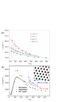
The knowledge of isotope effects on thermal transport properties is valuable for tuning heat conduction in graphene. Natural abundance carbon materials are made up of two stable isotopes of 12C (98.9%) and 13C (1.1%). Changing isotope composition can modify dynamic properties of crystal lattices and affect their thermal conductivity.HuJN-10APL ; Lindsay-13PRB For instance, it has been found that at room temperature isotopically purified diamond has a thermal conductivity of 3300 Wm-1K-1,Anthony-90PRB ; Berman-92PRB about 50% higher than that of natural diamond, 2200 Wm-1K-1.Ho-72JPCRD Similar effects have also been observed in 1D nanostructures, boron nitride nanotubes.ChangCW-06PRL Very recently, the first experimental work to show the isotope effect on graphene thermal conduction was reported by Chen et al.ChenSS-12NM By using the CVD technique, they synthesized isotopically modified graphene containing various percentages of 13C. The graphene flakes were subsequently suspended over 2.8-m-diameter holes and thermal conductivity was measured by the Raman thermometry technique. As shown in Figure 4a, compared with natural abundance graphene (1.1% 13C), the values were enhanced in isotopically purified samples (0.01% 13C), and reduced in isotopically mixed ones (50% 13C).
Isotope effects influence thermal conduction in two aspects: (i) modify phonon dispersion and (ii) introduce isotope scattering. We will analyze the two contributions separately for graphene.
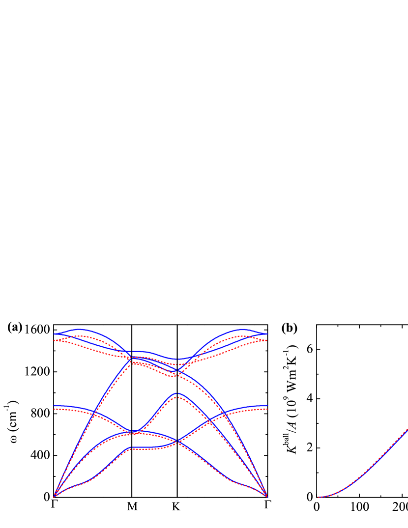
Figure 5a shows phonon dispersions for graphene systems comprising isotopically pure 12C and 13C. The replacement of 12C by 13C lowers frequencies of phonons. Such effects are negligible for low-frequency acoustic modes and become noticeable for high-frequency optical modes. In contrast, no observable frequency shift happens when varying the 13C isotope concentration from 0 to the natural abundance of 1.1% (see Figure 5a and Figure 3a).
The isotope-induced frequency shift can be detected by Raman experiments. Two types of Raman peaks are measured in graphene: the G peak corresponding to the doubly degenerated LO and TO mode at the point ( symmetry), and the 2D peak associated with the TO phonons nearby the K point.ferrari06prl ; malard09pr As shown in Figure 5a, when changing the atomic mass from 12 to 13, the TO and LO modes at the point shift from 1561 to 1500 cm-1, and the TO mode at the K point shifts from 1321 to 1269 cm-1. It is known that the frequency of optical phonons at the point is proportional to . This tells us that the frequency would decrease by when varying from 12 to 13. Both calculations predict a red shift of 61 cm-1 in the G peak, in good agreement with experiment (about 64 cm-1).ChenSS-12NM
The isotope-induced change in phonon dispersion may affect ballistic thermal conductance. To see the effects, we calculate as a function of for graphene with and 13, and present the results in Figure 5b. Interestingly, the two different give essentially the same . This is easy to understand in the Landauer picture. The isotope-induced frequency shifts are small in magnitude and are limited to the high-frequency region. Both features, independent of materials types, result in minor changes in . The unimportant isotope effect on should apply generally to other materials. This implies that the isotope-induced change in thermal conductivity comes from isotope scattering.
Isotope impurities as point defects are characterized by foreign atoms with different from host atoms. The variance in atomic mass causes phonon scattering, which is usually described as Rayleigh scattering. The scattering rate is , where , is the average atomic mass, is the phonon wavelength, and the exponent for 2D (3D) systems.klemens55 ; klemens94carbon ; klemens00 The formula states that isotope scattering mainly influences short-wavelength phonons, keeping long-wavelength phonons unaffected. The isotope scattering has minor influence on thermal conduction at very low temperatures when only low-frequency acoustic phonons are thermally excited, as well as at very high temperatures when electron-phonon and phonon-phonon interactions dominate phonon scattering. The isotope scattering could affect thermal conduction significantly provided that other scattering processes are relatively weak. For graphene, we expect important isotope effects on thermal conductivity in high-quality samples of large grains at intermediate temperatures.
The above theoretical picture is well supported by the experiment by Chen et al., ChenSS-12NM whose main results are shown in Figure 4a. They measured graphene samples with the 13C isotope concentration = 0.01%, 1.1%, 50% and 99.2%, and found that the room-temperature is about 4419, 2792, 2197 and 2816 Wm-1K-1, respectively. of the natural abundance is close to that of . While is insensitive to the average atomic mass, it can be tuned largely by varying the concentration of isotope impurity. Compared to the natural abundance system, room-temperature is lowered by 21% when increasing to 50%, and enhanced by 58% when decreasing to 0.01%. The enhancement becomes smaller with increasing temperature, as other scattering processes (like many-body scattering) become dominated. At K, of is about 2000 Wm-1K-1, 25% higher than that of .
Then we compare graphene with other materials. At room temperature, the isotopic enrichment induced enhancement of in graphene (58%) is comparable to those obtained in diamond (50%) Anthony-90PRB ; Berman-92PRB and boron nitride nanotubes (50%), ChangCW-06PRL and larger than those achieved in silicon (10%) kremer04ssc and germanium (30%). asen97prb The large enhancement of diamond and boron nitride nanotubes, as for graphene, is presumably because the experimental samples have low defect concentrations. It is known that isotope scattering would be overridden by other defect scattering processes in samples with high defect concentrations. The observation of large isotope effects on thermal conductivity could serve as an indication of high sample quality.
V.2 Structural Defect Effects
Structural defects are common in fabricated graphene, especially in CVD grown graphene.Wood-11NaL ; Koepke-13ACSN The effects of wrinklesChenSS-12NaT and grain sizeVlassiouk-11NaT on the thermal conduction of suspended single-layer CVD graphene have been examined in experiments by using the Raman thermometry technique. Chen et al.ChenSS-12NaT found that the thermal conductivity of graphene with obvious wrinkles (indicated by arrows in the inset of Figure 4b) is about 15-30% lower than that of wrinkle-free graphene over their measured temperature range, 330-520 K (Figure 4b). Vlassiouk et al.Vlassiouk-11NaT measured suspended graphene with different grain sizes obtained by changing the temperature of CVD growth. The grain sizes were estimated to be 150 nm, 38 nm, and 1.3 nm in different samples in terms of the intensity ratio of the G peak to D peak in Raman spectra.Cancado-06APL Since grain boundaries in graphene serve as extended defects and scatter phonons, graphene with smaller grain sizes are expected to suffer more frequent phonon scattering. Their measured thermal conductivity does show a decrease for smaller grain sizes, indicating the observation of the grain boundary effect on thermal conduction. Whereas, the dependence on the grain size shows a weak power law, , for which there is no theoretical explanation yet.Vlassiouk-11NaT However, for SiO2-supported graphene, recent theoretical work based on NEGF method showed a similar but stronger dependence of on the grain size in the range of m.Serov-13APL Further experimental studies are required to reveal the grain size effects on the thermal transport of both suspended and supported graphene.
Point defect scattering is usually described as Rayleigh scattering, which as shown above mainly affects transport of short-wavelength phonon modes. The influence of point defects on thermal transport has been extensively studied in theoretical works for various types of defects in graphene, including Stone-Wales defects, hao11apl ; haskins11an ; xie2011thermal substitutional defects, mortazavi12ssc ; jiang11apl and vacancies. zhang11prb ; hao11apl ; haskins11an ; jiang11apl In contrast, extended defects attracted less attention, bagri11nl ; lu12apl ; Serov-13APL ; HuangHQ-13PRB although in experiments they ubiquitously exist probably caused by substrate imperfections or kinetic factors coraux09njp ; park10carbon and can be precisely controlled nowadays. lahiri10nn Distinct from point defects, extended defects could induce a significant suppression of phonon transmission in a wide frequency range, leading to a large decrease in thermal conductance. Serov-13APL ; HuangHQ-13PRB While the defect-induced thermal conductance reduction moderately changes with varying defect types, it sensitively depends on the orientation between the extended defect and the transport direction. HuangHQ-13PRB
V.3 Substrate Effects in Supported Graphene
For practical applications, graphene is usually attached to a substrate in electronic and optoelectronic devices, so it is important to understand substrate effects on thermal properties of supported graphene OngZY-11PRB ; chen12nanoscale ; xu2012heat ; guo2012substrate . Seol et al.Seol-10S ; Seol-10JHT measured exfoliated SLG on a 300 nm thick SiO2 membrane by using the micro-resistance thermometry technique with the suspended bridge platform (Figure 1c). The observed thermal conductivity is 600 Wm-1K-1 near room temperature (solid black circles in Figure 2a). This value is much lower than those reported for suspended SLG via the Raman thermometry technique, but is still relatively high compared with those of bulk silicon (150 Wm-1K-1) and copper (400 Wm-1K-1). Another study by Cai et al.CaiWW-10NaL showed CVD SLG supported on Au also has a decreased thermal conductivity, 370 Wm-1K-1 (this lower value compared to 600 Wm-1K-1 could be caused by grain boundary scattering in CVD grapheneSerov-13APL ). The thermal conductivity reduction in supported graphene is attributed to substrate scattering, which strongly affects the out-of-plane flexural (ZA) mode of graphene.Seol-10S ; OngZY-11PRB ; QiuB-12APL This effect becomes stronger in encased graphene, where graphene is sandwiched between bottom and top SiO2. The thermal conductivity of SiO2-encased exfoliated SLG was measured to be below 160 Wm-1K-1, reported by Jang et al.Jang-10NaL using the micro-resistance thermometry technique with the substrate-supported platform (Figure 1e). For encased graphene, besides the phonon scattering by bottom and top oxides, the evaporation of top oxide could cause defects in graphene, which can further lower thermal conductivity. Knowing encased graphene is useful for analyzing heat dissipation in top-gated graphene devices. Similar to suspended graphene, the intrinsic phonon MFP for supported graphene can be estimated based on Equation (3). Since the graphene flakes measured by Seol et al.Seol-10S ; Seol-10JHT are very long (10 m) and relatively wide (m), approaching the diffusive regime, their values could be treated as for supported graphene. Combined with GWm-2K-1 at 300 K,XuY-09APL ; Bae-13NC ; Serov-13APL the backscattering of supported graphene is about 140 nm (or 90 nm for common MFP).Bae-13NC
V.4 Size Effects and Boundary Scattering
In macroscopic bulk materials, thermal conductance satisfies Fourier’s scaling law in the diffusive region, , where is an intrinsic material property, independent of system size. The scaling law could break down in nanostructures caused by two mechanisms: (i) thermal transport is not diffusive; and (ii) boundary effects become important.
For non-diffusive transport, becomes length dependent. It is proportional to as in the ballistic limit, gets saturated in the diffusive limit, and typically grows gradually with increasing in the intermediate region. When quantum interference effects become important, phonons may transport in the localization region, accompanied by an exponentially decayed transmission. The localization effects, however, are difficult to observe in experiments, since thermal conduction is contributed by many phonon modes, whose localization lengths are strongly frequency dependent. Savic-08PRL
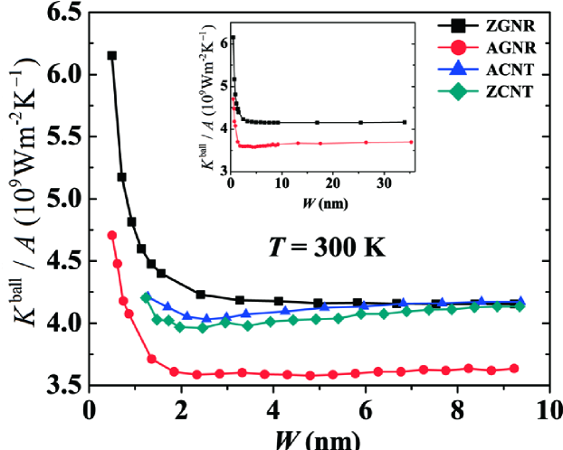
In nanostructures, boundary effects cannot be neglected, and gets dependent on . is no longer constant as in the bulk but dependent on due to boundary effects, and also depends on because the strength of boundary scattering varies with . A previous work systematically studied of GNRs with different ribbon widths and edge shapes using the NEGF method. XuY-09APL The main results are shown in Figure 6. As increases, has a signifiant decrease when nm and changes slowly with when nm. The room-temperature of GNRs with zigzag edges is about Wm-2K-1, close to those of graphene and CNTs.Mingo-05PRL In contrast, GNRs with armchair edges have obviously lower , displaying an interesting anisotropy in ballistic thermal conduction. The anisotropy can be as large as 30%, which could be further enhanced by modifying the edge shape. HuangHQ-13PRB The anisotropic generally exists in narrow GNRs and is expected to disappear when nm. Considering that graphene, as their bulk counterpart, is isotropic in thermal conduction (basal-plane), such an anisotropy obviously comes from boundary effects, which could be very long-range for phonon transport. We expect similar anisotropy in other materials. Anisotropic ballistic thermal conduction is also found in silicon nanowires (SiNWs) but was explained by the anisotropy of the bulk phonon dispersion. markussen08nl
In practice edges of graphene samples are not atomically regular but rather rough. The edge roughness causes phonon scattering and decreases . The phonon MFP associated with boundary scattering generally is described as . ziman2001 ; nika09prb ; Balandin-11NM is the dimension of the sample perpendicular to the transport direction, and for GNRs here. is an empirical parameter defined as the probability of specular scattering at the boundary. In the extremely rough limit (), , corresponding to fully diffusive scattering at the boundary. In general, is determined by the roughness of boundary and is between 0 and 1.
Boundary scattering could be a dominated scattering process in nanostructures, although it is usually unimportant in large samples. Silicon serves as an excellent example on this aspect. Bulk silicon has a large room-temperature of 150 Wm-1K-1 and nm as shown above. When nanostructuring silicon into nanowires, decreases seriously with respect to the bulk counterpart by about 100 fold. LiDY-03APL ; Hochbaum-08N ; Boukai-08N As is very similar between bulk jeong11jap and nanowires, markussen08nl SiNWs actually have about 100-fold smaller than the bulk. The results are quite amazing. By simply nanostructuring the material, thermal conductivity can be lowered orders of magnitude. This has strong implications to thermoelectrics. For instance, the thermoelectric figure of merit improves by 100 times through nanostructuring silicon into SiNWs, mainly contributed by the decrease of . Hochbaum-08N ; Boukai-08N
By developing the substrate-supported thermometry platform (Figure 1f), Bae et al.Bae-13NC for the first time measured the size effects on thermal transport in SiO2-supported, exfoliated graphene whose length and width are comparable to phonon MFP ( 140 nm as shown above). The obtained room temperature of 260-nm-long graphene is 320 Wm-1K-1, obviously lower than that of 10-m-long graphene reported by Seol et al.Seol-10S (Figure 7a). The data from these two studies can be captured by the simple model of length-dependent thermal conductivityBae-13NC ; Munoz-10NaL
| (4) |
with choices of simulated for SiO2-supported graphene by Seol et al.Seol-10S (see Figure 7b). As shown in Figure 7c, the corresponding thermal conductance per unit cross-sectional area, reaches 30-35% of theoretical ballistic upper limit up to room temperature for 260-nm-long graphene, indicating the quasi-ballistic transport (). The ballistic percentage is consistent with a simple estimation of transmission probability, , using sample length and back-scattering MFP nm for SiO2-supported graphene. This is the first time of observing quasi-ballistic thermal transport at room temperature in any materials, enabled by the relatively large phonon MFP of graphene. Previous observations of ballistic thermal transport were only at very low temperature (1 K).Schwab-00N
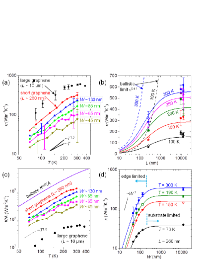
Bae et al.Bae-13NC further etched short (260 nm) graphene into arrays of nanoribbons (Figure 1f), whose width 45-130 nm, comparable to (140 nm). The observed thermal conductance changes back to the diffusive regime gradually as the GNR width decreases from 130 nm to 45 nm (Figure 7c), correspondingly decreases from 320 to 80 Wm-1K-1 at room temperature (Figure 7a), due to increased edge scattering in narrower GNRs. Experimental versus can be fitted with an empirical modelBae-13NC
| (5) |
where is the root-mean-square (r.m.s.) edge roughness and is given by Equation (4) and Figure 7b. As shown by the solid lines in Figure 7d, the best-fit exponent for all listed temperatures is , and this nearly dependence in edge-limited regime is consistent with previous findings for rough nanowires.ChenRK-08PRL ; Martin-09PRL ; Martin-10NaL ; Sadhu-11PRB The simple model appears to be a good approximation in a regime with , but it is likely to change in a situation with extremely rough edges, where the roughness correlation lengthLim-12NaL and phonon localizationWangY-12APL could also play an important role. Thus, deeper understandings of and scalings due to edge-roughness scattering still require further theoretical studies and experimental observations. It is worth noting that through the electrical breakdown measurement on GNRs derived from unzipped CNTs,Kosynkin-09N ; JiaoLY-09N ; HuangB-09JACS ; HuangB-10JCP Liao et al.LiaoA-11PRL was able to estimate GNR , and their values are slightly higher than those of Bae et al.Bae-13NC for similar widths. Considering that CNT-unzipped GNRs have smoother edges,Kosynkin-09N ; JiaoLY-09N the two studies are essentially consistent.
V.5 Interlayer Effects in Few-Layer Graphene
Interlayer scattering as well as top and bottom boundary scattering could take place in few-layer graphene, which could be another mechanism to modulate graphene thermal conductivity. It is interesting to investigate the evolution of the thermal conductivity of FLG with increasing thickness, denoted by the number of atomic layers (), and the critical thickness needed to recover the thermal conductivity of graphite.
Several experimental studies on this topic have been conducted for encased,Jang-10NaL supported,Sadeghi-13PNAS and suspended FLG,Ghosh-10NM ; Jang-13APL and their results are summarized in Figure 8. Jang et al.Jang-10NaL measured the thermal transport of SiO2-encased FLG by using the substrate-supported, micro-resistance thermometry platform (Figure 1e). They found that the room-temperature thermal conductivity increases from 50 to 1000 Wm-1K-1 as the FLG thickness increases from 2 to 21 layers, showing a trend to recover natural graphite . This strong thickness dependence was explained by the top and bottom boundary scattering and disorder penetration into FLG induced by the evaporated top oxide.Jang-10NaL Very recently, another similar yet less pronounced trend was observed in SiO2-supported FLG by Sadeghi et al.Sadeghi-13PNAS using the suspended micro-resistance thermometry platform (similar to Figure 1c). As shown by red dots in Figure 8, the measured room-temperature increases slowly as increasing thickness, and the recovery to natural graphite would occur even more than 34 layers. The difference between the results by Jang et al.Jang-10NaL and Sadeghi et al.Sadeghi-13PNAS is not unexpected, because encased FLG could be suppressed much more in thin layers than thick layers due to the effect of top oxide, and hence shows a stronger thickness dependence.
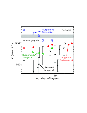
For suspended FLG, there are two contradictory observations in the thickness dependence. At first, based on the Raman thermometry technique (Figure 1a) Ghosh et al.Ghosh-10NM showed a decrease of suspended FLG from the SLG high value to regular graphite value as thickness increases from 2 to 8 layers (open diamonds in Figure 8). The reduction was explained by the interlayer coupling and increased phase-space states available for the phonon Umklapp scattering in thicker FLG.Ghosh-10NM However, a very recent study by Jang et al.Jang-13APL seems to show a different thickness trend for suspended FLG. They measured thermal conductivity of suspended graphene of 2-4 and 8 layers by using a modified T-bridge micro-resistance thermometry technique. The obtained room-temperature for 2-4 layers is about 300-400 Wm-1K-1 with no apparent thickness dependence, while for 8-layer shows an increase to 600 Wm-1K-1 (open squares in Figure 8). Surprisingly, this trend is qualitatively in agreement with that of Sadeghi et al.Sadeghi-13PNAS for supported FLG; both show similar increasing amounts of from 2 to 8 layers (Figure 8), despite a small decrease from 2 to 4 layers in the former, which could arise from different sample qualities and measurement uncertainty. Given opposite thickness trends of Ghosh et al.Ghosh-10NM and Jang et al.,Jang-13APL further experimental works are required to clarify the real thickness-dependent in suspended FLG. Moreover, we want to point out that suspended FLG values of Jang et al.Jang-13APL are close to those reported by Pettes et al.Pettes-11NaL for suspended bilayer graphene (BLG), 600 Wm-1K-1 at room temperature (see Figure 2a). Both are much lower than suspended SLG . The latter attributed this to phonon scattering by a residual polymeric layer on graphene,Pettes-11NaL even though the former claimed that electrical current annealing was used to remove polymer residues.Jang-13APL
V.6 Cross-Plane Thermal Conduction
A remarkable feature of graphite and graphene is that their thermal properties are highly anisotropic. Despite high thermal conductivity along the in-plane direction, heat flow along the cross-plane direction (c axis) is hundreds of times weaker, limited by weak van der Waals interactions between layers (for graphite) or with adjacent materials (for graphene). For example, the thermal conductivity along the c axis of pyrolytic graphite is only 6 Wm-1K-1 at room temperatureHo-72JPCRD (Figure 2a). For graphene, it is often attached to a substrate or embedded in a medium for potential applications. Heat conduction along the cross-plane direction is characterized by the thermal interface/boundary conductance between graphene and adjacent materials, which could become a limiting dissipation bottleneck in highly scaled graphene devices and interconnects.Pop-12MRSB ; Bae-10NaL ; Bae-11ACSN ; Behnam-12NaL ; Islam-13EDL
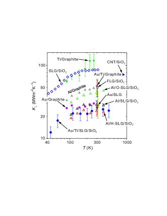
The thermal interface conductance across graphene/graphite and other materials has been measured by using 3 method,ChenZ-09APL time-domain thermoreflectance (TDTR) technique,Mak-10APL ; Schmidt-10JAP ; Norris-12JHT ; Koh-10NaL ; Hopkins-12NaL ; ZhangCW-13Carbon and Raman-based method,CaiWW-10NaL ; Ermakov-13NaT Most experimental data available to date are shown in Figure 9, and they are consistent with each other in general, given the variations of sample qualities and measurement techniques. Chen et al.ChenZ-09APL and Mak et al.Mak-10APL showed the thermal interface conductance per unit area of graphene/SiO2 is MWm-2K-1 at room temperature, with no strong dependence on the FLG thickness. Their values are close to that of CNT/SiO2,Pop-07JAP reflecting the similarity between graphene and CNT. Schmidt et al.Schmidt-10JAP measured of the graphite/metal interfaces, including Au, Cr, Al, and Ti. Among them, the graphite/Ti has the highest , 120 MWm-2K-1, and the graphite/Au interface has the lowest , 30 MWm-2K-1 near room temperature. Their of graphite/Au is consistent with the value by Norris et al.Norris-12JHT and values of SLG/Au by Cai et al.CaiWW-10NaL and FLG/Au by Ermakov et al.Ermakov-13NaT Koh et al.Koh-10NaL later measured heat flow across the Au/Ti/-LG/SiO2 interfaces with the layer number . Their observed room-temperature is 25 MWm-2K-1, which shows a very weak dependence on the layer number and is equivalent to the total thermal conductance of Au/Ti/graphite and graphene/SiO2 interfaces acting in series. This indicates that the thermal resistance of two interfaces between graphene and its environment dominates over that between graphene layers. Interestingly, Hopkins et al.Hopkins-12NaL showed the thermal conduction across the Al/SLG/SiO2 interface could be manipulated by introducing chemical adsorbates between the Al and SLG. As shown in Figure 9, their measured of untreated Al/SLG/SiO2 is 30 MWm-2K-1 at room temperature, in agreement with Zhang et al.ZhangCW-13Carbon The increases to 42 MWm-2K-1 for oxygen-functionalized graphene (O-SLG), while decreases to 23 MWm-2K-1 for hydrogen-functionalized graphene (H-SLG). These effects were attributed to changes in chemical bonding between the metal and graphene, and are consistent with the observed enhancement in from the Al/diamondStoner-92PRL to Al/O-diamond interfaces.Collins-10APL
VI Thermoelectric Properties of Graphene
Thermoelectric materials can convert waste heat into electricity by the Seebeck effect and use electricity to drive electronic cooling or heating by the Peltier effect. Thermoelectric devices are all-solid-state devices with no moving part, thus are silent, reliable and scalable. However, they only find limited applications due to their low efficiency. The efficiency of a thermoelectric material is determined by the thermoelectric figure of merit (), which typically is defined as goldsmid1986
| (6) |
where is the electrical conductivity, is the Seebeck coefficient [also called thermoelectric power (TEP) or thermopower], is the absolute temperature, and the thermal conductivity have contributions from electrons () and lattice vibrations (). is usually extracted based on the Wiedemann-Franz Law , where the Lorenz number is equal to WK-2 for free electrons. This law does not always hold. For example, becomes zero for a delta-shaped transport distribution. mahan1996best However, in graphene is negligible with respect to , Saito-07PRB ; Watanabe-09PRB ; Balandin-08NaL ; Fong-13PRX ; Yigen-13PRB ; Yigen-14NaL similar as in CNTs. Hone-99PRB ; Kim-01PRL Currently, the state-of-art commercial thermoelectric materials, like Bi2Ti3, have room-temperature around 1. Snyder-08NM
Two important concepts have been developed to guide thermoelectrics research in the last twenty years. Dresselhaus-07AM ; Snyder-08NM One was proposed by Hicks and Dresselhaus in 1993, which suggests to improve by going to lower dimensions. hicks1993-2D ; hicks1993-1D Based on this concept, significant enhancements of to larger than 1 are found, for instance, in thin films venkatasubramanian01science and in quantum dot superlattices. harman02science The other concept, demonstrated by two seminal experiments in 2008, Hochbaum-08N ; Boukai-08N suggests to increase by nanostructuring. The experiments found a 100-fold increase of in SiNWs over the bulk counterpart, mainly attributed to the decrease of induced by boundary scattering. Graphene nanostructures can naturally combine the two concepts and might be useful for thermoelectrics research and applications.
For realizing large in graphene systems, two major disadvantages have to be overcome: (i) is too high; (ii) is too small due to the gapless band structure. In the above section, we discussed various approaches to tune thermal conduction in graphene. Among them, boundary scattering, that can largely decrease as demonstrated in SiNWs, is a promising way. Previous theoretical calculations predict that GNRs with disordered edge structures sevinccli10prb or graphene quantum dots XuY-10PRB may support large . In addition, introducing weakly coupled interfaces can block thermal conduction efficiently. Taking CNTs as an example, despite extremely large of single CNTs, when they are formed into random networks,Estrada-11APL ; Behnam-12ACSN ; Timmermans-12NaR ; Gupta-12JAP ; Gupta-13NaT theoretical simulations predicted ultra small of 0.13-0.2 Wm-1K-1 for networks due to junctions between CNTs. prasher09prl The same concept could be used for graphene to reduce . Next, we mainly discuss the Seebeck effect in graphene.
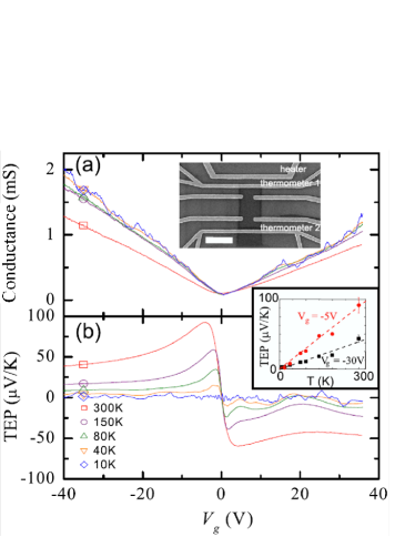
Thermoelectric transport in graphene has been experimentally investigated in the past five years.Zuev-09PRL ; WeiP-09PRL ; Checkelsky-09PRB ; WangCR-10PRB ; Nam-10PRB ; Nam-13PRL ; WangDQ-11PRB ; LiuXF-12SSC ; WuXS-11APL ; Babichev-13JAP ; XuXD-10NaL ; Grosse-11NN The Seebeck coefficient and electrical conductance of graphene can be measured against the gate voltage (thus, carrier density ) simultaneously via a widely-used microfabricated structure (inset of Figure 10a), which was developed by Small et al.Small-03PRL to measure thermoelectric transport in CNTs. Figure 10 shows typical results of measured and as a function of in graphene at different temperatures.Zuev-09PRL The Seebeck coefficient shows two peaks near the Dirac point (charge neutrality point) and changes its sign across the Dirac point as the majority carrier switches from electron to hole. The room-temperature peak values of for SLG and BLG are observed to be 50-100 VK-1 in different experiments.Zuev-09PRL ; WeiP-09PRL ; Checkelsky-09PRB ; WangCR-10PRB ; Nam-10PRB For high carrier density (i.e., high ), the measured Seebeck coefficient scales as for SLG due to its linear dispersion,WeiP-09PRL while for BLG due to its hyperbolic dispersion,WangCR-10PRB consistent with theories. Importantly, the simultaneous measurements of and enable testing the validation of the semiclassical Mott relation:Cutler-69PR
| (7) |
where is the Boltzmann constant, is the electron charge, and is the Fermi energy. For SLG the measured shows a linear dependence (inset of Figure 10b) and matches calculated from measured by Equation (7),Zuev-09PRL ; WeiP-09PRL ; Checkelsky-09PRB indicating an agreement with the Mott relation. For BLG, however, the agreement only holds for high carrier density; for low carrier density there is an obvious difference between measured and calculated as well as a deviation from the linear dependence at high temperature.WangCR-10PRB ; Nam-10PRB This failure of the Mott relation was attributed to the low Fermi temperature in BLG.
The thermoelectric properties of materials can be also probed by using a conducting tip to measure the thermoelectric voltage between the sample and tip, induced by a given temperature difference between them. By employing atomic force microscopy (AFM) and scanning tunneling microscopy (STM) techniques, Cho et al.Cho-13NM and Park et al.ParkJ-13NaL measured the thermopower of epitaxial graphene on SiC, respectively. The advantage of this method is the simultaneous imaging of the sample structure and thermoelectric signals with a spatial resolution of atomic-scale. Since the Seebeck coefficient relies on the sample local density of states (LDOS) near the Fermi energy, and LDOS can be quite different in the presence of boundaries and disordersOuYangFP-08JPCC ; HuangB-08JPCC ; LiJ-10PRB ; LinF-09CPL ; li2012dirac , thermoelectric imaging allows us to probe grain boundaries, wrinkles, defects, and impurities in graphene, which may not be reflected in topography images.Cho-13NM ; ParkJ-13NaL
For practical applications, the Seebeck coefficient and power factor of graphene should be improved. Some experimental efforts have been made in this direction. Wang et al.WangCR-11PRL observed enhanced below room temperature in a dual-gated BLG device, resulting from the opening of a band gap by applying a perpendicular electric field on BLG. Additionally, the Seebeck coefficient and power factor of FLG could be enhanced at high temperature ( 500 K) by molecular attachmentsSim-11JPCC and oxygen plasma treatment,XiaoN-11ACSN attributed to the band gap opening. By constructing the c-axis preferentially oriented nanoscale Sb2Te3 film on monolayer graphene, both and were increased, benefiting from a highway for carriers provided by graphene.Hong-12PCCP From a practical point of view, Hewitt et al.Hewitt-12SM focused on maximizing the power output of FLG/polyvinylidene fluoride composite thin films by considering the absolute temperature, temperature gradient, load resistance, and physical dimensions of films.
VII Summary and Outlook
In summary, graphene is one of the best heat conductors in nature. The exceptionally high thermal conductivity appears in graphene caused by a combination of several unique features, specifically, its low dimension, light atomic mass, and strong covalent bonding. Important isotope effects have been found in graphene, evidencing the weak strength of other scattering processes. Moreover, strong size effects and (quasi-)ballistic thermal transport at room temperature have been observed in graphene due to its long phonon MFP.
We also show possible ways to shorten the phonon MFP, including coupling to a substrate, constructing narrow GNRs with rough boundaries, introducing weakly coupled interfaces, etc. These approaches helps us decrease thermal conductivity of graphene for thermal insulation and thermoelectric applications. We finally discuss the challenges of using graphene for thermoelectrics and possible strategies to overcome the challenges.
Significant progresses have been made in researches on thermal conduction in graphene in the past few years. However, there are still some important fundamental problems unresolved. For example, the change of the scattering strength induced by low dimension has not been well studied. Many quantum effects, like coherent scattering and weak localization, might be important in thermal transport but remain almost unknown (at least in experiments). Whether Fourier’s law holds in low-dimensional systems or not is still a controversial issue, and what are the key factors to drive ballistic-diffusive transport is not well understood. On thermoelectrics, the enhancement of requires suppressing thermal conduction while keeping electrical conduction less affected. More works are deserved for designing approaches to effectively decouple electrons and phonons.
We acknowledge the support of the Ministry of Science and Technology of China (Grant Nos. 2011CB921901 and 2011CB606405), and the National Natural Science Foundation of China (Grant No. 11334006).
References
- (1) A. K. Geim and K. S. Novoselov, Nat. Mater. 6, 183 (2007)
- (2) A. H. Castro Neto, F. Guinea, N. M. R. Peres, K. S. Novoselov, and A. K. Geim, Rev. Mod. Phys. 81, 109 (2009)
- (3) S. D. Sarma, S. Adam, E. Hwang, and E. Rossi, Rev. Mod. Phys. 83, 407 (2011)
- (4) A. A. Balandin, Nat. Mater. 10, 569 (2011)
- (5) A. A. Balandin, S. Ghosh, D. Nika, and E. Pokatilov, Fuller. Nanotub. Carbon Nanostruct. 18, 474 (2010)
- (6) A. A. Balandin, Advancing Microelectronics 38, 6 (2011)
- (7) D. L. Nika and A. A. Balandin, J. Phys.: Condens. Matter 24, 233203 (2012)
- (8) M. M. Sadeghi, M. T. Pettes, and L. Shi, Solid State Commun. 152, 1321 (2012)
- (9) E. Pop, V. Varshney, and A. K. Roy, MRS Bulletin 37, 1273 (2012)
- (10) A. A. Balandin and D. L. Nika, Mater. Today 15, 266 (2012)
- (11) K. M. Shahil and A. A. Balandin, Solid State Commun. 152, 1331 (2012)
- (12) L. Shi, Nanoscale Microscale Thermophys. Eng. 16, 79 (2012)
- (13) A. A. Balandin, S. Ghosh, W. Bao, I. Calizo, D. Teweldebrhan, F. Miao, and C. Lau, Nano Lett. 8, 902 (2008)
- (14) S. Lepri, R. Livi, and A. Politi, Phys. Rep. 377, 1 (2003)
- (15) G. Basile, C. Bernardin, and S. Olla, Phys. Rev. Lett. 96, 204303 (2006)
- (16) A. Casher and J. Lebowitz, J. Math. Phys. 12, 1701 (1971)
- (17) A. Lippi and R. Livi, J. Stat. Phys. 100, 1147 (2000)
- (18) A. Dhar, Phys. Rev. Lett. 86, 5882 (2001)
- (19) L. Yang, Phys. Rev. Lett. 88, 094301 (2002)
- (20) O. Narayan and S. Ramaswamy, Phys. Rev. Lett. 89, 200601 (2002)
- (21) K. Saito and A. Dhar, Phys. Rev. Lett. 104, 040601 (2010)
- (22) B. Huang, Q. Yan, Z. Li, and W. Duan, Front. Phys. China 4, 269 (2009)
- (23) J. Bai and Y. Huang, Mater. Sci. Eng., R 70, 341 (2010)
- (24) J. Lan, J.-S. Wang, C. K. Gan, and S. K. Chin, Phys. Rev. B 79, 115401 (2009)
- (25) J.-W. Jiang, J. Lan, J.-S. Wang, and B. Li, J. Appl. Phys. 107, 054314 (2010)
- (26) Z. Li, H. Qian, J. Wu, B.-L. Gu, and W. Duan, Phys. Rev. Lett. 100, 206802 (2008)
- (27) Z. Li, B. Huang, and W. Duan, J. Nanosci. and Nanotechnol. 10, 5374 (2010)
- (28) D. Nika, E. Pokatilov, A. Askerov, and A. A. Balandin, Phys. Rev. B 79, 155413 (2009)
- (29) Y. Xu and W. Duan, in Nanoscale Energy Transport and Harvesting: A Computational Study, edited by G. Zhang (Pan Stanford Publishing, 2014)
- (30) E. Pop, S. Sinha, and K. Goodson, Proc. IEEE 94, 1587 (2006)
- (31) E. Pop, Nano Research 3, 147 (2010)
- (32) L. Pang, H.-C. Seo, P. Chapman, I. Adesida, and K. K. Kim, J. Electron. Mater. 39, 499 (2010)
- (33) L. Pang and K. K. Kim, J. Phys. D: Appl. Phys. 45, 045105 (2012)
- (34) L. Pang, Y. Lian, D.-S. Kim, J.-H. Lee, and K. Kim, IEEE Trans. Electron Devices 59, 2650 (2012)
- (35) A. Liao, R. Alizadegan, Z.-Y. Ong, S. Dutta, F. Xiong, K. J. Hsia, and E. Pop, Phys. Rev. B 82, 205406 (2010)
- (36) C.-L. Tsai, A. Liao, E. Pop, and M. Shim, Appl. Phys. Lett. 99, 053120 (2011)
- (37) M. S. Dresselhaus, G. Chen, M. Y. Tang, R. Yang, H. Lee, D. Wang, Z. Ren, J.-P. Fleurial, and P. Gogna, Adv. Mater. 19, 1043 (2007)
- (38) G. Snyder and E. Toberer, Nat. Mater. 7, 105 (2008)
- (39) S. Subrina, D. Kotchetkov, and A. A. Balandin, IEEE Electron Device Lett. 30, 1281 (2009)
- (40) Z. Yan, G. Liu, J. M. Khan, and A. A. Balandin, Nat. Commun. 3, 827 (2012)
- (41) K. M. F. Shahil and A. A. Balandin, Nano Lett. 12, 861 (2012)
- (42) V. Goyal and A. A. Balandin, Appl. Phys. Lett. 100, 073113 (2012)
- (43) P. Goli, S. Legedza, A. Dhar, R. Salgado, J. Renteria, and A. A. Balandin, J. Power Sources 248, 37 (2014)
- (44) W. J. Evans, L. Hu, and P. Keblinski, Appl. Phys. Lett. 96, 203112 (2010)
- (45) Z.-Y. Ong and E. Pop, Phys. Rev. B 84, 075471 (2011)
- (46) J. Hu, Y. Wang, A. Vallabhaneni, X. Ruan, and Y. P. Chen, Appl. Phys. Lett. 99, 113101 (2011)
- (47) N. Yang, X. Ni, J.-W. Jiang, and B. Li, Appl. Phys. Lett. 100, 093107 (2012)
- (48) G. Zhang and H. Zhang, Nanoscale 3, 4604 (2011)
- (49) L. Lindsay, D. Broido, and N. Mingo, Phys. Rev. B 82, 115427 (2010)
- (50) L. Lindsay, D. Broido, and N. Mingo, Phys. Rev. B 82, 161402 (2010)
- (51) L. Lindsay, D. Broido, and N. Mingo, Phys. Rev. B 83, 235428 (2011)
- (52) Z. Aksamija and I. Knezevic, Appl. Phys. Lett. 98, 141919 (2011)
- (53) Z. Aksamija and I. Knezevic, Phys. Rev. B 86, 165426 (2012)
- (54) Y. Xu, X. Chen, B.-L. Gu, and W. Duan, Appl. Phys. Lett. 95, 233116 (2009)
- (55) Y. Xu, X. Chen, J.-S. Wang, B.-L. Gu, and W. Duan, Phys. Rev. B 81, 195425 (2010)
- (56) J.-W. Jiang, B.-S. Wang, and J.-S. Wang, Appl. Phys. Lett. 98, 113114 (2011)
- (57) Y. Lu and J. Guo, Appl. Phys. Lett. 101, 043112 (2012)
- (58) A. Y. Serov, Z.-Y. Ong, and E. Pop, Appl. Phys. Lett. 102, 033104 (2013)
- (59) K. Saito, J. Nakamura, and A. Natori, Phys. Rev. B 76, 115409 (2007)
- (60) S. Datta, Electronic Transport in Mesoscopic Systems (Cambridge University Press, Cambridge, 1997)
- (61) Y. Xu, J.-S. Wang, W. Duan, B.-L. Gu, and B. Li, Phys. Rev. B 78, 224303 (2008)
- (62) C. Jeong, R. Kim, M. Luisier, S. Datta, and M. Lundstrom, J. Appl. Phys. 107, 023707 (2010)
- (63) L. G. C. Rego and G. Kirczenow, Phys. Rev. Lett. 81, 232 (1998)
- (64) K. Schwab, E. Henriksen, J. Worlock, and M. Roukes, Nature 404, 974 (2000)
- (65) M.-H. Bae, Z. Li, Z. Aksamija, P. N. Martin, F. Xiong, Z.-Y. Ong, I. Knezevic, and E. Pop, Nat. Commun. 4, 1734 (2013)
- (66) E. Watanabe, S. Yamaguchi, J. Nakamura, and A. Natori, Phys. Rev. B 80, 085404 (2009)
- (67) K. C. Fong, E. E. Wollman, H. Ravi, W. Chen, A. A. Clerk, M. Shaw, H. Leduc, and K. Schwab, Phys. Rev. X 3, 041008 (2013)
- (68) S. Yiğen, V. Tayari, J. O. Island, J. M. Porter, and A. R. Champagne, Phys. Rev. B 87, 241411 (2013)
- (69) S. Yiğen and A. R. Champagne, Nano Lett. 14, 289 (2014)
- (70) S. Ghosh, D. L. Nika, E. P. Pokatilov, and A. A. Balandin, New J. Phys. 11, 095012 (2009)
- (71) W. Cai, A. L. Moore, Y. Zhu, X. Li, S. Chen, L. Shi, and R. S. Ruoff, Nano Lett. 10, 1645 (2010)
- (72) J. H. Seol, I. Jo, A. L. Moore, L. Lindsay, Z. H. Aitken, M. T. Pettes, X. Li, Z. Yao, R. Huang, D. Broido, N. Mingo, R. S. Ruoff, and L. Shi, Science 328, 213 (2010)
- (73) M. T. Pettes, I. Jo, Z. Yao, and L. Shi, Nano Lett. 11, 1195 (2011)
- (74) W. Jang, Z. Chen, W. Bao, C. N. Lau, and C. Dames, Nano Lett. 10, 3909 (2010)
- (75) D. G. Cahill, K. Goodson, and A. Majumdar, J. Heat Transf. 124, 223 (2002)
- (76) C. D. S. Brites, P. P. Lima, N. J. O. Silva, A. Millan, V. S. Amaral, F. Palacio, and L. D. Carlos, Nanoscale 4, 4799 (2012)
- (77) S. Ghosh, I. Calizo, D. Teweldebrhan, E. P. Pokatilov, D. L. Nika, A. A. Balandin, W. Bao, F. Miao, and C. N. Lau, Appl. Phys. Lett. 92, 151911 (2008)
- (78) S. Ghosh, W. Bao, D. L. Nika, S. Subrina, E. P. Pokatilov, C. N. Lau, and A. A. Balandin, Nat. Mater. 9, 555 (2010)
- (79) J.-U. Lee, D. Yoon, H. Kim, S. W. Lee, and H. Cheong, Phys. Rev. B 83, 081419 (2011)
- (80) S. Chen, A. L. Moore, W. Cai, J. W. Suk, J. An, C. Mishra, C. Amos, C. W. Magnuson, J. Kang, L. Shi, and R. S. Ruoff, ACS Nano 5, 321 (2011)
- (81) S. Chen, Q. Wu, C. Mishra, J. Kang, H. Zhang, K. Cho, W. Cai, A. A. Balandin, and R. S. Ruoff, Nat. Mater. 11, 203 (2012)
- (82) S. Chen, Q. Li, Q. Zhang, Y. Qu, H. Ji, R. S. Ruoff, and W. Cai, Nanotechnology 23, 365701 (2012)
- (83) C. Faugeras, B. Faugeras, M. Orlita, M. Potemski, R. R. Nair, and A. K. Geim, ACS Nano 4, 1889 (2010)
- (84) I. Vlassiouk, S. Smirnov, I. Ivanov, P. F. Fulvio, S. Dai, H. Meyer, M. Chi, D. Hensley, P. Datskos, and N. V. Lavrik, Nanotechnology 22, 275716 (2011)
- (85) V. A. Ermakov, A. V. Alaferdov, A. R. Vaz, A. V. Baranov, and S. A. Moshkalev, Nanotechnology 24, 155301 (2013)
- (86) K. F. Mak, C. H. Lui, and T. F. Heinz, Appl. Phys. Lett. 97, 221904 (2010)
- (87) Y. K. Koh, M.-H. Bae, D. G. Cahill, and E. Pop, Nano Lett. 10, 4363 (2010)
- (88) P. E. Hopkins, M. Baraket, E. V. Barnat, T. E. Beechem, S. P. Kearney, J. C. Duda, J. T. Robinson, and S. G. Walton, Nano Lett. 12, 590 (2012)
- (89) C. Zhang, W. Zhao, K. Bi, J. Ma, J. Wang, Z. Ni, Z. Ni, and Y. Chen, Carbon 64, 61 (2013)
- (90) Z. Chen, W. Jang, W. Bao, C. N. Lau, and C. Dames, Appl. Phys. Lett. 95, 161910 (2009)
- (91) J. H. Seol, I. Jo, Z. Yao, A. L. Moore, and L. Shi, J. Heat Transf. 133, 022403 (2010)
- (92) Z. Wang, R. Xie, C. T. Bui, D. Liu, X. Ni, B. Li, and J. T. L. Thong, Nano Lett. 11, 113 (2011)
- (93) M. M. Sadeghi, I. Jo, and L. Shi, Proc. Natl. Acad. Sci. U.S.A. 110, 16321 (2013)
- (94) W. Jang, W. Bao, L. Jing, C. N. Lau, and C. Dames, Appl. Phys. Lett. 103, 133102 (2013)
- (95) V. E. Dorgan, A. Behnam, H. J. Conley, K. I. Bolotin, and E. Pop, Nano Lett. 13, 4581 (2013)
- (96) H. Xie, L. Chen, W. Yu, and B. Wang, Appl. Phys. Lett. 102, 111911 (2013)
- (97) Y.-J. Yu, M. Y. Han, S. Berciaud, A. B. Georgescu, T. F. Heinz, L. E. Brus, K. S. Kim, and P. Kim, Appl. Phys. Lett. 99, 183105 (2011)
- (98) M. E. Pumarol, M. C. Rosamond, P. Tovee, M. C. Petty, D. A. Zeze, V. Falko, and O. V. Kolosov, Nano Lett. 12, 2906 (2012)
- (99) F. Menges, H. Riel, A. Stemmer, C. Dimitrakopoulos, and B. Gotsmann, Phys. Rev. Lett. 111, 205901 (2013)
- (100) R. R. Nair, P. Blake, A. N. Grigorenko, K. S. Novoselov, T. J. Booth, T. Stauber, N. M. R. Peres, and A. K. Geim, Science 320, 1308 (2008)
- (101) L. Yang, J. Deslippe, C.-H. Park, M. L. Cohen, and S. G. Louie, Phys. Rev. Lett. 103, 186802 (2009)
- (102) K. S. Kim, Y. Zhao, H. Jang, S. Y. Lee, J. M. Kim, K. S. Kim, J.-H. Ahn, P. Kim, J.-Y. Choi, and B. H. Hong, Nature 457, 706 (2009)
- (103) V. G. Kravets, A. N. Grigorenko, R. R. Nair, P. Blake, S. Anissimova, K. S. Novoselov, and A. K. Geim, Phys. Rev. B 81, 155413 (2010)
- (104) K. F. Mak, J. Shan, and T. F. Heinz, Phys. Rev. Lett. 106, 046401 (2011)
- (105) A. C. Ferrari and D. M. Basko, Nat. Nanotech. 8, 235 (2013), and references therein
- (106) L. Shi, D. Li, C. Yu, W. Jang, D. Kim, Z. Yao, P. Kim, and A. Majumdar, J. Heat Transf. 125, 881 (2003)
- (107) A. L. Moore and L. Shi, Meas. Sci. Technol. 22, 015103 (2011)
- (108) P. Kim, L. Shi, A. Majumdar, and P. L. McEuen, Phys. Rev. Lett. 87, 215502 (2001)
- (109) C. Yu, L. Shi, Z. Yao, D. Li, and A. Majumdar, Nano Lett. 5, 1842 (2005)
- (110) C. W. Chang, A. M. Fennimore, A. Afanasiev, D. Okawa, T. Ikuno, H. Garcia, D. Li, A. Majumdar, and A. Zettl, Phys. Rev. Lett. 97, 085901 (2006)
- (111) C. Chang, D. Okawa, H. Garcia, A. Majumdar, and A. Zettl, Phys. Rev. Lett. 101, 75903 (2008)
- (112) M. T. Pettes and L. Shi, Adv. Funct. Mater. 19, 3918 (2009)
- (113) J. Yang, Y. Yang, S. W. Waltermire, T. Gutu, A. A. Zinn, T. T. Xu, Y. Chen, and D. Li, Small 7, 2334 (2011)
- (114) D. Li, Y. Wu, P. Kim, L. Shi, P. Yang, and A. Majumdar, Appl. Phys. Lett. 83, 2934 (2003)
- (115) A. Hochbaum, R. Chen, R. Delgado, W. Liang, E. Garnett, M. Najarian, A. Majumdar, and P. Yang, Nature 451, 163 (2008)
- (116) A. Boukai, Y. Bunimovich, J. Tahir-Kheli, J. Yu, W. Goddard Iii, and J. Heath, Nature 451, 168 (2008)
- (117) R. Chen, A. I. Hochbaum, P. Murphy, J. Moore, P. Yang, and A. Majumdar, Phys. Rev. Lett. 101, 105501 (2008)
- (118) J. Lim, K. Hippalgaonkar, S. C. Andrews, A. Majumdar, and P. Yang, Nano lett. 12, 2475 (2012)
- (119) C. Y. Ho, R. W. Powell, and P. E. Liley, J. Phys. Chem. Ref. Data 1, 279 (1972)
- (120) E. Pop, D. Mann, Q. Wang, K. Goodson, and H. Dai, Nano Lett. 6, 96 (2006)
- (121) D. L. Nika, A. S. Askerov, and A. A. Balandin, Nano Lett. 12, 3238 (2012)
- (122) N. Mingo and D. A. Broido, Nano Lett. 5, 1221 (2005)
- (123) J. P. Perdew, K. Burke, and M. Ernzerhof, Phys. Rev. Lett. 77, 3865 (1996)
- (124) G. Kresse and J. Furthmüller, Phys. Rev. B 54, 11169 (1996)
- (125) N. Bonini, J. Garg, and N. Marzari, Nano Lett. 12, 2673 (2012)
- (126) D. L. Nika, E. P. Pokatilov, and A. A. Balandin, Phys. Status Solidi B 248, 2609 (2011)
- (127) A. I. Cocemasov, D. L. Nika, and A. A. Balandin, Phys. Rev. B 88, 035428 (2013)
- (128) P. Y. Yu and M. Cardona, Fundamentals of Semiconductors: Physics and Materials Properties, 2nd ed. (Springer-Verlag, Berlin, 1999)
- (129) N. Mingo and D. A. Broido, Phys. Rev. Lett. 95, 096105 (2005)
- (130) C. Jeong, S. Datta, and M. Lundstrom, J. Appl. Phys. 109, 073718 (2011)
- (131) Y. Xu, B. Yan, H.-J. Zhang, J. Wang, G. Xu, P. Tang, W. Duan, and S.-C. Zhang, Phys. Rev. Lett. 111, 136804 (2013)
- (132) H. J. Goldsmid, Electronic Refrigeration, Vol. 76 (Pion London, 1986)
- (133) D. Nika, S. Ghosh, E. Pokatilov, and A. A. Balandin, Appl. Phys. Lett. 94, 203103 (2009)
- (134) A. Fasolino, J. Los, and M. I. Katsnelson, Nat. Mater. 6, 858 (2007)
- (135) X. Li, K. Maute, M. L. Dunn, and R. Yang, Phys. Rev. B 81, 245318 (2010)
- (136) H. Zhu, Y. Xu, B.-L. Gu, and W. Duan, New J. Phys. 14, 013053 (2012)
- (137) X. Chen, Y. Xu, X. Zou, B.-L. Gu, and W. Duan, Phys. Rev. B 87, 155438 (2013)
- (138) G. A. Slack, Phys. Rev. 127, 694 (1962)
- (139) C. N. Hooker, A. R. Ubbelohde, and D. A. Young, Proc. R. Soc. Lond. A 284, 17 (1965)
- (140) R. Taylor, Philos. Mag. 13, 157 (1966)
- (141) J. Hu, S. Schiffli, A. Vallabhaneni, X. Ruan, and Y. P. Chen, Appl. Phys. Lett. 97, 133107 (2010)
- (142) L. Lindsay, D. Broido, and T. Reinecke, Phys. Rev. B 88, 144306 (2013)
- (143) T. R. Anthony, W. F. Banholzer, J. F. Fleischer, L. Wei, P. K. Kuo, R. L. Thomas, and R. W. Pryor, Phys. Rev. B 42, 1104 (1990)
- (144) R. Berman, Phys. Rev. B 45, 5726 (1992)
- (145) A. Ferrari, J. Meyer, V. Scardaci, C. Casiraghi, M. Lazzeri, F. Mauri, S. Piscanec, D. Jiang, K. Novoselov, S. Roth, et al., Phys. Rev. Lett. 97, 187401 (2006)
- (146) L. Malard, M. Pimenta, G. Dresselhaus, and M. Dresselhaus, Phys. Rep. 473, 51 (2009)
- (147) P. Klemens, Proc. Phys. Soc. A 68, 1113 (1955)
- (148) P. Klemens and D. Pedraza, Carbon 32, 735 (1994)
- (149) P. Klemens, J. Wide Bandgap Mater. 7, 332 (2000)
- (150) R. Kremer, K. Graf, M. Cardona, G. Devyatykh, A. Gusev, A. Gibin, A. Inyushkin, A. Taldenkov, and H.-J. Pohl, Solid State Commun. 131, 499 (2004)
- (151) M. Asen-Palmer, K. Bartkowski, E. Gmelin, M. Cardona, A. Zhernov, A. Inyushkin, A. Taldenkov, V. Ozhogin, K. Itoh, and E. Haller, Phys. Rev. B 56, 9431 (1997)
- (152) J. D. Wood, S. W. Schmucker, A. S. Lyons, E. Pop, and J. W. Lyding, Nano Lett. 11, 4547 (2011)
- (153) J. C. Koepke, J. D. Wood, D. Estrada, Z.-Y. Ong, K. T. He, E. Pop, and J. W. Lyding, ACS Nano 7, 75 (2013)
- (154) L. Cancado, K. Takai, T. Enoki, M. Endo, Y. Kim, H. Mizusaki, A. Jorio, L. Coelho, R. Magalhaes-Paniago, and M. Pimenta, Appl. Phys. Lett. 88, 163106 (2006)
- (155) F. Hao, D. Fang, and Z. Xu, Appl. Phys. Lett. 99, 041901 (2011)
- (156) J. Haskins, A. Kınacı, C. Sevik, H. Sevincli, G. Cuniberti, and T. Cagın, ACS Nano 5, 3779 (2011)
- (157) Z.-X. Xie, K.-Q. Chen, and W. Duan, J. Phys.: Condens. Matter 23, 315302 (2011)
- (158) B. Mortazavi, A. Rajabpour, S. Ahzi, Y. Rémond, and S. Mehdi Vaez Allaei, Solid State Commun. 152, 261 (2012)
- (159) H. Zhang, G. Lee, and K. Cho, Phys. Rev. B 84, 115460 (2011)
- (160) A. Bagri, S.-P. Kim, R. S. Ruoff, and V. B. Shenoy, Nano Lett. 11, 3917 (2011)
- (161) H. Huang, Y. Xu, X. Zou, J. Wu, and W. Duan, Phys. Rev. B 87, 205415 (2013)
- (162) J. Coraux, M. Engler, C. Busse, D. Wall, N. Buckanie, F.-J. M. Zu Heringdorf, R. Van Gastel, B. Poelsema, T. Michely, et al., New J. Phys. 11, 023006 (2009)
- (163) H. J. Park, J. Meyer, S. Roth, and V. Skákalová, Carbon 48, 1088 (2010)
- (164) J. Lahiri, Y. Lin, P. Bozkurt, I. I. Oleynik, and M. Batzill, Nat. Nanotech. 5, 326 (2010)
- (165) J. Chen, G. Zhang, and B. Li, Nanoscale 5, 532 (2012)
- (166) Z. Xu and M. J. Buehler, J. Phys.: Condens. Matter 24, 475305 (2012)
- (167) Z.-X. Guo, J. Ding, and X.-G. Gong, Phys. Rev. B 85, 235429 (2012)
- (168) B. Qiu and X. Ruan, Appl. Phys. Lett. 100, 193101 (2012)
- (169) I. Savić, N. Mingo, and D. A. Stewart, Phys. Rev. Lett. 101, 165502 (2008)
- (170) T. Markussen, A.-P. Jauho, and M. Brandbyge, Nano Lett. 8, 3771 (2008)
- (171) J. M. Ziman, Electrons and Phonons: the Theory of Transport Phenomena in Solids (Oxford University Press, 2001)
- (172) E. Munoz, J. Lu, and B. I. Yakobson, Nano Lett. 10, 1652 (2010)
- (173) P. Martin, Z. Aksamija, E. Pop, and U. Ravaioli, Phys. Rev. Lett. 102, 125503 (2009)
- (174) P. N. Martin, Z. Aksamija, E. Pop, and U. Ravaioli, Nano Lett. 10, 1120 (2010)
- (175) J. Sadhu and S. Sinha, Phys. Rev. B 84, 115450 (2011)
- (176) Y. Wang, B. Qiu, and X. Ruan, Appl. Phys. Lett. 101, 013101 (2012)
- (177) D. V. Kosynkin, A. L. Higginbotham, A. Sinitskii, J. R. Lomeda, A. Dimiev, B. K. Price, and J. M. Tour, Nature 458, 872 (2009)
- (178) L. Jiao, L. Zhang, X. Wang, G. Diankov, and H. Dai, Nature 458, 877 (2009)
- (179) B. Huang, Y.-W. Son, G. Kim, W. Duan, and J. Ihm, J. Am. Chem. Soc. 131, 17919 (2009)
- (180) B. Huang, Z. Li, Y.-W. Son, G. Kim, W. Duan, and J. Ihm, J. Chem. Phys. 133, 084702 (2010)
- (181) A. D. Liao, J. Z. Wu, X. Wang, K. Tahy, D. Jena, H. Dai, and E. Pop, Phys. Rev. Lett. 106, 256801 (2011)
- (182) M.-H. Bae, Z.-Y. Ong, D. Estrada, and E. Pop, Nano Lett. 10, 4787 (2010)
- (183) M.-H. Bae, S. Islam, V. E. Dorgan, and E. Pop, ACS Nano 5, 7936 (2011)
- (184) A. Behnam, A. S. Lyons, M.-H. Bae, E. K. Chow, S. Islam, C. M. Neumann, and E. Pop, Nano Lett. 12, 4424 (2012)
- (185) S. Islam, Z. Li, V. Dorgan, M.-H. Bae, and E. Pop, IEEE Electron Device Lett. 34, 166 (2013)
- (186) E. Pop, D. A. Mann, K. E. Goodson, and H. Dai, J. Appl. Phys. 101, 093710 (2007)
- (187) A. J. Schmidt, K. C. Collins, A. J. Minnich, and G. Chen, J. Appl. Phys. 107, 104907 (2010)
- (188) P. M. Norris, J. L. Smoyer, J. C. Duda, and P. E. Hopkins, J. Heat Transf. 134, 020910 (2012)
- (189) R. J. Stoner, H. J. Maris, T. R. Anthony, and W. F. Banholzer, Phys. Rev. Lett. 68, 1563 (1992)
- (190) K. C. Collins, S. Chen, and G. Chen, Appl. Phys. Lett. 97, 083102 (2010)
- (191) G. Mahan and J. Sofo, Proc. Natl. Acad. Sci. 93, 7436 (1996)
- (192) J. Hone, M. Whitney, C. Piskoti, and A. Zettl, Phys. Rev. B 59, 2514 (1999)
- (193) L. Hicks and M. Dresselhaus, Phys. Rev. B 47, 12727 (1993)
- (194) L. Hicks and M. Dresselhaus, Phys. Rev. B 47, 16631 (1993)
- (195) R. Venkatasubramanian, E. Siivola, T. Colpitts, and B. O’quinn, Nature 413, 597 (2001)
- (196) T. Harman, P. Taylor, M. Walsh, and B. LaForge, Science 297, 2229 (2002)
- (197) H. Sevinçli and G. Cuniberti, Phys. Rev. B 81, 113401 (2010)
- (198) D. Estrada and E. Pop, Appl. Phys. Lett. 98, 073102 (2011)
- (199) A. Behnam, V. K. Sangwan, X. Zhong, F. Lian, D. Estrada, D. Jariwala, A. J. Hoag, L. J. Lauhon, T. J. Marks, M. C. Hersam, and E. Pop, ACS Nano 7, 482 (2012)
- (200) M. Y. Timmermans, D. Estrada, A. G. Nasibulin, J. D. Wood, A. Behnam, D.-m. Sun, Y. Ohno, J. W. Lyding, A. Hassanien, E. Pop, and E. I. Kauppinen, Nano Research 5, 307 (2012)
- (201) M. P. Gupta, L. Chen, D. Estrada, A. Behnam, E. Pop, and S. Kumar, J. Appl. Phys. 112, 124506 (2012)
- (202) M. P. Gupta, A. Behnam, F. Lian, D. Estrada, E. Pop, and S. Kumar, Nanotechnology 24, 405204 (2013)
- (203) R. S. Prasher, X. Hu, Y. Chalopin, N. Mingo, K. Lofgreen, S. Volz, F. Cleri, and P. Keblinski, Phys. Rev. Lett. 102, 105901 (2009)
- (204) Y. M. Zuev, W. Chang, and P. Kim, Phys. Rev. Lett. 102, 096807 (2009)
- (205) P. Wei, W. Bao, Y. Pu, C. N. Lau, and J. Shi, Phys. Rev. Lett. 102, 166808 (2009)
- (206) J. G. Checkelsky and N. P. Ong, Phys. Rev. B 80, 081413 (2009)
- (207) C.-R. Wang, W.-S. Lu, and W.-L. Lee, Phys. Rev. B 82, 121406 (2010)
- (208) S.-G. Nam, D.-K. Ki, and H.-J. Lee, Phys. Rev. B 82, 245416 (2010)
- (209) S.-G. Nam, E. H. Hwang, and H.-J. Lee, Phys. Rev. Lett. 110, 226801 (2013)
- (210) D. Wang and J. Shi, Phys. Rev. B 83, 113403 (2011)
- (211) X. Liu, Z. Ma, and J. Shi, Solid State Commun. 152, 469 (2012)
- (212) X. Wu, Y. Hu, M. Ruan, N. K. Madiomanana, C. Berger, and W. A. de Heer, Appl. Phys. Lett. 99, 133102 (2011)
- (213) A. V. Babichev, V. E. Gasumyants, and V. Y. Butko, J. Appl. Phys. 113, 076101 (2013)
- (214) X. Xu, N. M. Gabor, J. S. Alden, A. M. van der Zande, and P. L. McEuen, Nano Lett. 10, 562 (2010)
- (215) K. L. Grosse, M.-H. Bae, F. Lian, E. Pop, and W. P. King, Nat. Nanotech. 6, 287 (2011)
- (216) J. P. Small, K. M. Perez, and P. Kim, Phys. Rev. Lett. 91, 256801 (2003)
- (217) M. Cutler and N. F. Mott, Phys. Rev. 181, 1336 (1969)
- (218) S. Cho, S. D. Kang, W. Kim, E.-S. Lee, S.-J. Woo, K.-J. Kong, I. Kim, H.-D. Kim, T. Zhang, J. A. Stroscio, Y.-H. Kim, and H.-K. Lyeo, Nat. Mater. 12, 913 (2013)
- (219) J. Park, G. He, R. M. Feenstra, and A.-P. Li, Nano Lett. 13, 3269 (2013)
- (220) F. OuYang, B. Huang, Z. Li, J. Xiao, H. Wang, and H. Xu, J. Phys. Chem. C 112, 12003 (2008)
- (221) B. Huang, Z. Li, Z. Liu, G. Zhou, S. Hao, J. Wu, B.-L. Gu, and W. Duan, J. Phys. Chem. C 112, 13442 (2008)
- (222) J. Li, Z. Li, G. Zhou, Z. Liu, J. Wu, B.-L. Gu, J. Ihm, and W. Duan, Phys. Rev. B 82, 115410 (2010)
- (223) F. Lin, G. Zhou, Z. Li, J. Li, J. Wu, and W. Duan, Chem. Phys. Lett. 475, 82 (2009)
- (224) Y. Li, P. Chen, G. Zhou, J. Li, J. Wu, B.-L. Gu, S. B. Zhang, and W. Duan, Phys. Rev. Lett. 109, 206802 (2012)
- (225) C.-R. Wang, W.-S. Lu, L. Hao, W.-L. Lee, T.-K. Lee, F. Lin, I.-C. Cheng, and J.-Z. Chen, Phys. Rev. Lett. 107, 186602 (2011)
- (226) D. Sim, D. Liu, X. Dong, N. Xiao, S. Li, Y. Zhao, L.-J. Li, Q. Yan, and H. H. Hng, J. Phys. Chem. C 115, 1780 (2011)
- (227) N. Xiao, X. Dong, L. Song, D. Liu, Y. Tay, S. Wu, L.-J. Li, Y. Zhao, T. Yu, H. Zhang, W. Huang, H. H. Hng, P. M. Ajayan, and Q. Yan, ACS Nano 5, 2749 (2011)
- (228) S. Hong, E. S. Kim, W. Kim, S.-J. Jeon, S. C. Lim, K. H. Kim, H.-J. Lee, S. Hyun, D. Kim, J.-Y. Choi, Y. H. Lee, and S. Baik, Phys. Chem. Chem. Phys. 14, 13527 (2012)
- (229) C. A. Hewitt and D. L. Carroll, Synth. Met. 162, 2379 (2012)