HERMES: A Hierarchical Broadcast-Based Silicon Photonic Interconnect for Scalable Many-Core Systems
Abstract
Optical interconnection networks, as enabled by recent advances in silicon photonic device and fabrication technology, have the potential to address on-chip and off-chip communication bottlenecks in many-core systems. Although several designs have shown superior power efficiency and performance compared to electrical alternatives, these networks will not scale to the thousands of cores required in the future.
In this paper, we introduce Hermes, a hybrid network composed of an optimized broadcast for power-efficient low-latency global-scale coordination and circuit-switch sub-networks for high-throughput data delivery. This network will scale for use in thousand core chip systems. At the physical level, SoI-based adiabatic coupler has been designed to provide low-loss and compact optical power splitting. Based on the adiabatic coupler, a topology based on 2-ary folded butterfly is designed to provide linear power division in a thousand core layout with minimal cross-overs. To address the network agility and provide for efficient use of optical bandwidth, a flow control and routing mechanism is introduced to dynamically allocate bandwidth and provide fairness usage of network resources. At the system level, bloom filter-based filtering for localization of communication are designed for reducing global traffic. In addition, a novel greedy-based data and workload migration are leveraged to increase the locality of communication in a NUCA (non-uniform cache access) architecture. First order analytic evaluation results have indicated that Hermes is scalable to at least 1024 cores and offers significant performance improvement and power savings over prior silicon photonic designs.
I Introduction
With the advent of multi-core architectures, communication will become a bottleneck for tomorrow’s systems. Processing power is growing exponentially, following Moore’s law, through integration of more cores on-chip, putting more pressure on global communication. However, electrical interconnects have failed to keep pace. Rather, according to International Technology Roadmap for Semiconductors (ITRS) projections, electrical interconnects have evolved to be power inefficient and a performance hindrance [1]. Even looking at future prospects of different system, we see high-bandwidth low-latency networks as the gateway for high performance and power efficiency. RAMCloud for example proposes using DRAM as main storage for memory instead of hard-drives which would be used for backup. The electrical interconnect path connecting processor to DRAM and processors to each other will stand in the way of realization of RAMCloud for cloud computing [2].
The emerging technology of silicon photonics has been proposed as an alternative solution to on-chip and off-chip communication [3, 4, 5]. Not only does silicon photonics offer light-speed relay-free communication and high bandwidth, in addition, it serves as an ultra-low-power network backplane. As a demonstration of silicon photonics potential, several on-chip networks have been proposed to solve on-chip communication problem [6, 7, 8, 9, 10]. Different topologies, flow control, and routing mechanisms have been introduced. For instance, bus-based broadcast have been shown to be superior to electrical alternatives [11, 12]. Crossbars were later introduced to further reduce power and improve bandwidth of the system [6, 7]. Hybrid electrical-optical networks have been introduced to offer the arbitration mechanism and circumvent bufferless routing in optical interconnects [10, 8, 9]. However, these architectures suffer from a common problem: scalability.
We predict, along with several experts in the architecture domain, that future microprocessors will constitute tens to hundreds of cores in the same package [5, 13, 14]. With such large scale systems current silicon photonics designs are are not designed with such scale in mind and thus do not provide the performance requirements nor satisfy the power constraints. Bus-based broadcast topologies, for instance, exhibit an exponential power growth with number of cores [11, 6]. Hybrid optical-electrical networks suffer from the power inefficiency of electrical interconnects [8, 9, 10]. Finally, the widely-used serpentine-shaped crossbars exhibit a linearly increasing latency and power with number of cores [7, 15, 6].
In this work, we propose Hermes, a hierarchical scalable silicon photonic interconnect for large-scale systems, which addresses both performance and power concerns for thousand core systems. The network is composed of:
-
•
Broadcast Network: The network is a hybrid network consisting of a novel high-bandwidth, low-latency optical broadcast network for arbitration and communication. Unlike existing broadcast networks, this broadcast network is scalable to large core-count with near ideal power division and delivery. With such a broadcast structure one can improve the performance of the system which is sensitive to latency of broadcast packets. Even if only a small percentage of total traffic is broadcast, it can degrade the whole system performance if not handled properly [16].
-
•
Linear Network: The broadcast-network is augmented with a circuit-switch optical network for long, throughput-hungry messages. This linear point-to-point networK is designed to improve bandwidth for local communication.
-
•
Hierarchical communication domains: The hierarchical approach divides communication into local and global domains. This hierarchical approach allows the scalability of the system to thousand core with minimal power overhead. However, to enable efficient operation and high performance, communication should be limited to local domains. Novel greedy-based data and workload migration techniques to minimize communication in the global domain and reduce latency. In addition, at the global-local interface we use a bloom filter to filter requests that can be processed locally [17].
Hermes shows superior performance and power efficiency compared to prior silicon photonics designs [6, 5, 12, 3]. At the local communication domain, a linear-power scalability is achieved as a result of the novel optimized broadcast network presented. Moreover, the latency is minimized to match direct point to point latency. As for bandwidth, the circuit-switch linear network is optimized with that goal in mind. It dynamically allocates bandwidth and allows high bandwidth point to point communication for long cache-line messages. On the other hand, at the global communication domain, latency is minimized by Hermes’ locality-improving techniques. First order evaluations show that Hermes can greatly improve the latency and bandwidth of the system at low power level compared to other networks in the literature that are designed for tens of cores.
This study focuses on scalability of silicon photonic on-chip networks for thousand-core systems, making the following contributions:
-
•
A novel hierarchical high-bandwidth and low-power network for communication in future thousand-core systems.
-
•
Silicon photonic is a new field and the design abstraction levels are not well defined which lead to incorrect assumptions and designs. This study addresses the design problem at different design levels including device-level, physical-layout, topology, flow control, and system-level optimizations. Moreover, we attempt to provide a device-level analysis for abstraction at higher levels of design.
The rest of the paper is organized as follows: Section II presents the background for this work. Next, we discuss the proposed design in Section IV. In Section V we describe our evaluation methodology and present our results then we conclude in Section VI.
II Background
Advances in silicon photonics have enabled integration of optical devices on a chip with high density. The integration of silicon photonic devices has been leveraged in on-chip interconnect to replace copper interconnects. In this section we present a brief overview of the structure of silicon photonic interconnects in general. In addition, we also discuss the design of thousand-core system and how to overcome the main challenges facing its realization [5, 13, 14].
II-A Basic components
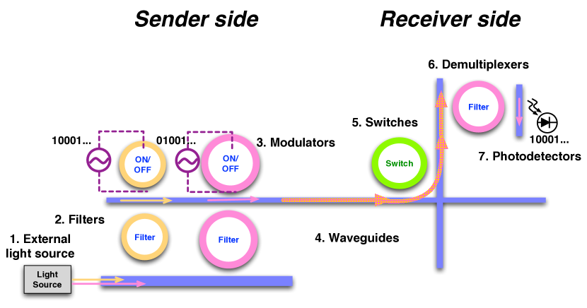
The optical path in the silicon photonic network-on-chip mimics its counterpart in telecommunication as shown in Figure 1. The optical path starts with a laser-source which will be located off-chip into the foreseeable future [18]. The next stage is a filter that divides the broadband optical light into different channels in the frequency domain [19]. These channels provide the necessary bandwidth through wave-division-multiplexing (WDM) which waveguides cannot provide through space-division-multiplexing (SDM). SDM is widely used by running multiple waveguides in parallel to increase bandwidth. In the stage following filters, the demultiplexed channels are modulated with the digital stream of data and carried on a waveguide [20, 21, 22, 23]. The waveguide is the conduit for the optical signal across the chip. Along the optical path, the optical signal may encounter one or more switches that divert the path of the signal [24, 25, 26, 23]. In addition, it may encounter electro-optic conversion points for signal regeneration. Finally, it reaches a photodetector at the destination [27, 28, 29].
Individual silicon photonic components have been designed, fabricated, and characterized. The Emtnano team [30] have fabricated in Epixfab [31] several micro-ring based passive filters, modulators and wide-band switches. These devices have been measured, characterized, and modeled. The EMTNano team [30] measurements demonstrate high quality factor and compact footprint which makes it suitable for high density integration in optical on-chip interconnect. Other components have been fabricated and characterized by other groups such as thermo-optic micro-ring modulators having a power consumption that ranges from 7 fJ/bit [22] while electro-optic micro-rings have a power consumption of 86 fJ/bit [32] depending on the tuning techniques and switching speeds. Germanium-doped silicon photo-detectors have been demonstrated exhibiting low power, as low as 33 fJ/bit [32], and delivering over-GHz speed.
Based on the photonic devices, several groups have built optical links and characterized them. For instance, Chen et al. demonstrated an optical link operating at 3 Gbps and dissipating as low as 120 fJ/bit of optical power. Alduino et al. demonstrated a 4-channel WDM link operating at 10 Gbps with a maximum power dissipation of 900 fJ/bit of optical power [33]. Finally, Zheng et al. built a low-power optical link operating at 10 Gbps and dissipating a few hundred fJ/bit of optical power [34].
II-B Thousand core system design
We envision that future systems will be many-core systems sharing the same chip. The chip composed of hundreds to a thousand core and DRAM memory, will be integrated and interconnected. Integration will be 3 dimensional to integrate the cores, DRAM memory , and silicon photonics interconnect [35]. At the local-level, tens of chips are integrated and another layer of silicon photonics interconnects run between the domains and connects them together. The whole system can be a large distributed shared memory system enabled by our high bandwidth, low latency photonic communication backplane. Memory will be shared and distributed among processing and communication domains while caches located within each processing and communication domain will be shared locally at the local-level. Cache coherence for thousand core system is maintained by snoopy cache coherence leveraging our novel broadcast network.
Current silicon photonic networks do not scale to the thousand core architecture in latency, bandwidth, nor power. They are designed for low core count and do not account for problems arising in thousand core system as we show in Section V. This motivates our work presented here and our approach for on-chip network design in Hermes as we explain next.
III Network design
Current efforts in silicon photonics on-chip network design focus on architecture techniques with limited investigation in the device level. The abstraction of devices for silicon photonics on-chip network remains incomplete. This introduces invalid assumptions or limited exploitation of device capabilities. Herein, we attempt to bridge the gap between the device level and architecture design by focusing on broadcast-based design and the available power splitter options. More specifically, we give a device-level review of different devices, their characteristics and their impact on the architecture design. Then, we demonstrate how to exploit the capabilities of the device at the architecture level.
In this section, we explain the construction of the broadcast network. We follow a bottom-up approach starting from the power-splitter continuing upwards to the network design. We first compare between different alternatives for power-splitting and justify our choice for the adiabatic coupler. Next, we show the topology used for our broadcast network and how to place the different components in the on-chip layout. Following that, we discuss the topology and layout of the linear network. Finally, we explain how these networks interact to provide the communication backplane for a thousand-core system.
III-A Power-Splitter
In a broadcast network, the power splitter plays a crucial role in splitting the input power into equal beams. The device-level options vary in characteristics. The main characteristics of concern are bandwidth, insertion loss, CMOS compatibility, and splitting ratio of the output beams. Next, we survey different options for power-splitting and focus on the adiabatic coupler.
| Device | Antenna [36] | Y & Trench | Adiabatic |
|---|---|---|---|
| Splitter [37, 38] | Coupler [39] | ||
| Bandwidth | 1.35-1.65 m | 1.5-1.6 m | 1.5-1.6 m |
| Power efficiency | 23% | 80% | 96% |
| Number of ports | 64 | Any | Any |
| CMOS Compatible | Yes | No | Yes |
| Area | m2 | m2 | m2 |
| Process variation | Moderate | Sensitive | Insensitive |
Power splitting can be achieved by several means as shown in Table I. For example, an antenna array splits a single input to many outputs with a wide-wavelength-band operation. However, it suffers from low bandwidth and power inefficiency. A maximum of 64 ports can be designed and fabricated; beyond that, power efficiency and bandwidth degrade to an unacceptable point as simulations indicate. Moreover, the power efficiency of a 32-port antenna is 23% for minimum transmission. Consequently, the antenna array exhibits limited performance and power efficiency which calls for further innovation in one-to-many power splitters [36].
Y-splitters and trench-based splitters have been demonstrated as other options for power splitting. Y-splitters, on one hand, demonstrate sensitivity to fabrication inaccuracies. The minute dimensions challenge photolithography limits [37]. Hence, we exclude them from consideration in the near future. On the other hand, trench-based splitters suffer from low power efficiency, which can be as low as 80% [40, 38].
Adiabatic coupler, the device chosen for building our network, combines several advantages with low overhead:
-
•
Bandwidth: It has a wide wavelength band of operation that extends beyond the C+L band (1530-1625 nm). This wide band of operation adds another advantage which is immunity to thermal variations. Thermal variations that shift the bandwidth, lead to insignificant impact on the device characteristics due to its wide wavelength band.
- •
-
•
Insertion loss: The insertion loss of the adiabatic coupler is inherently negligible due to the adiabatic nature of the device. The only loss worth mentioning is the waveguide loss, which is 2.5 db/cm [31]
-
•
Number of ports: The number of ports is 2 outputs but can be extended to any number of ports by cascading the device to form a network as we will show in Hermes broadcast network.
-
•
CMOS compatibility: Cao et al. have successfully fabricated an adiabatic coupler in SOI and demonstrated the characteristics experimentally [39]. This confirms that adiabatic coupler can be successfully fabricated and integrated with CMOS process.
-
•
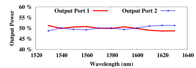
Immunity to process variation Our simulations shows that for worst case process variation (10% increase in waveguide width accompanied by decrease in gap width) shows a 45-55% power splitting across the C+L band. Hence, the splitting ration and bandwidth remain at high levels despite the change in design dimensions.
Another characteristic of adiabatic coupler that we have leveraged in our network design is reciprocity of the device as our simulation results indicate, which implies that the output and input ports can be exchanged while maintaining the same power splitting functionality. Moreover, the adiabatic coupler is a two-input, two-output device which makes it function as a wavelength-combiner in addition to splitter. That means that if two input ports have signals at different wavelengths, then the two signals will be split at the two output ports as if they had been combined at the input.
The only drawback of the adiabatic coupler compared to the other alternatives, is its relatively long dimension, which may reach 200 m [39] However, this drawback does not impact our design, since up to sixteen adiabatic couplers are used on-chip where area is scarce and this number can easily fit on-chip.
III-B Broadcast-network design
In this section we demonstrate how to connect the adiabatic coupler in order to achieve broadcast from one node to the others in a performance- and power- efficient manner. First, the topology is presented; following that, the layout is explained. Finally, we extend the design from a single waveguide to a high-bandwidth design, with an analysis of the involved trade-offs.
Our goal from the presented topology is to achieve a latency equivalent to point-to-point connection while having a high bandwidth as close as to bus and corssbar networks. Hermes broadcast can achieve a latency equivalent to point to point latency, where waveguides connecting the far ends of the chip run diagonally across layout. As for bandwidth, the bandwidth of Hermes is higher than traditional networks and can achieve close to bus- and crossbar- based bandwidth by running multiple waveguides in parallel. The only limitation on number of parallel waveguides is crossovers. We show how to reduce crossover loss in large bandwidth networks. These characteristics which we demonstrate in this section meets the ideal case we project in Section V-B.
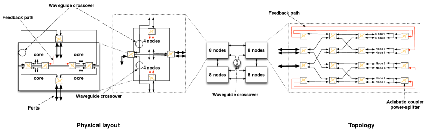
The basic topology of the network is similar to a folded 2-ary butterfly network with some adjustments as shown in Figure 3. Each link in the figure represents a two-way link. Each block in the diagram represents a two-input two-output adiabatic coupler. Each coupler serves as both a power-splitter (splits the input signal into two signal of equal length) and wavelength-combiner (combines the two input signals from different inputs to same output). The two-ary butterfly topology is folded network, carrying optical signal in both directions. However, there are alternate feedback paths shown in red to avoid the same wavelength traveling along the same optical link in different directions which may lead to interference. The topology including the butterfly topology and the alternate feedback paths form a power splitting network of levels as the minimum number of levels. It provides a near ideal-linear power division all-to-all broadcast network.
The layout of the network shown in Figure 3 depicts the placement of the adiabatic coupler on-chip and the routing of waveguides between the devices. In this layout each group of two processing cores connect to an adiabatic coupler forming a cluster. Each two neighboring cluster connect to the next level of the topology through another stage of adiabatic coupler forming a bigger cluster. After we reach a cluster of eight nodes these eight nodes are connected to the rest of the clusters through direct connections encountering a single waveguide crossover. In addition, feedback paths are provided as shown in red in Figure 3 which also have a maximum of two waveguide crossover. Hence, the maximum number of waveguide crossover along any optical path in this network is one waveguide crossover.
In order to achieve a high bandwidth network, more than one waveguide need to run in parallel. However, such a network can introduce excess loss at intersections. Hence, careful design of the intersections and number of waveguides is necessary. In this design, we use the waveguide-crossings designed by Popovic et al. [41]. The loss in this structure has been known to be as low as 0.045 dB/crossing. While the crosstalk is measured at -35 dB, this has a less pronounced impact on the system compared to the loss; therefore, in our analysis we focus on the crossing loss. For a hundred parallel waveguide, we get 4.5 dB providing a plethora of bandwidth with a small optical power penalty.
In case of high waveguide count, in order to reduce the number of crossovers in the network one may opt for extending the number of adiabatic coupler levels by more levels. This approach on one hand reduces the number of crossovers but introduces a 3 dB loss per extra level in the topology. Hence, a tradeoff between crossover loss versus adiabatic coupler excess loss requires careful design.
III-C Linear network
In this section, we describe the second part of the network, the linear network. This linear network serves as a medium for transferring long messages between nodes. Unlike earlier serpentine networks, this network in addition to providing point-to-point communication links, it favors local communication over global communication.
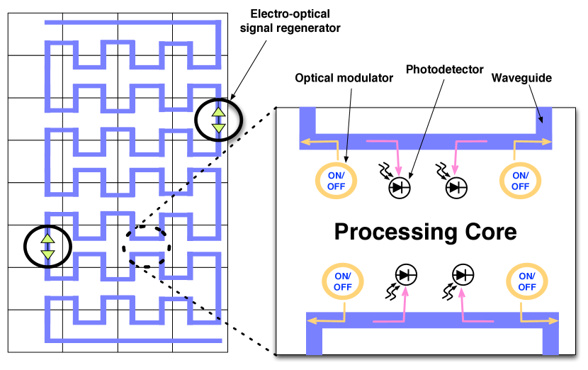
The goal we had in mind while designing this network was having high-bandwidth point-to-point communication links. Since, serpentine shaped networks have highest bandwidth, we follow the same topology; however, we propose changes to improve concurrency and overcome the high optical loss of these long waveguides. First, we change the topology from simple serpentine to the one we show in Figure 4. This topology gives more access points and reduces the distance between further nodes and improve local communication bandwidth. Hence, congestion is alleviated and concurrency is improved. Moreover, we add electro-optic conversion points to mitigate the optical loss and linearize it in terms of number of cores. Next, we discuss in detail the physical design of the linear network.
The layout of the network is shown in Figure 4. The waveguide runs in a serpentine shape across the chip crossing the same processing core twice. This layout does not introduce any crossings and allows a large number of parallel waveguides, improving the bandwidth of the network as required for the large packets transferred on this medium. Moreover, the network provides four access points for communication per node as shown in Figure 4. This increases concurrency because more than one path exists between communicating nodes. Finally, the topology of this network reduces the distance between neighboring nodes, favoring local communication over long-distance ones. This kind of locality can be exploited using kernel-level approaches leveraged in this design such as data migration [42] and workload migration [43].
Traditional techniques of designing long waveguides suffer from excessive waveguide losses and off-resonance coupling losses. Waveguide loss is attributed to the silicon loss of the waveguide, while off-resonance coupling loss occur when a non-resonant wavelength passes through the through port of the filter, switch, or modulator. To overcome these two limitations, we employ electro-optic conversion points. These points re-generate the signal by converting it to an electrical then back to optical signals. However, only two electro-optic points are employed introducing a small latency and power overhead. In addition, the packets on this network exhibit less sensitivity to latency and the optical power savings compensates the electrical power added. With electro-optic conversion, the longest optical path is 8 cm adding 20 dB of overall waveguide loss according to Epixfab fabrication process [31]. In addition, we leverage wide band switches that reduce the number of micro-rings and off-resonance coupling the optical signal needs to tolerate [24]. In our system, the maximum off-resonance coupling along any optical path is less than 4 dB.
III-D Hierarchical design
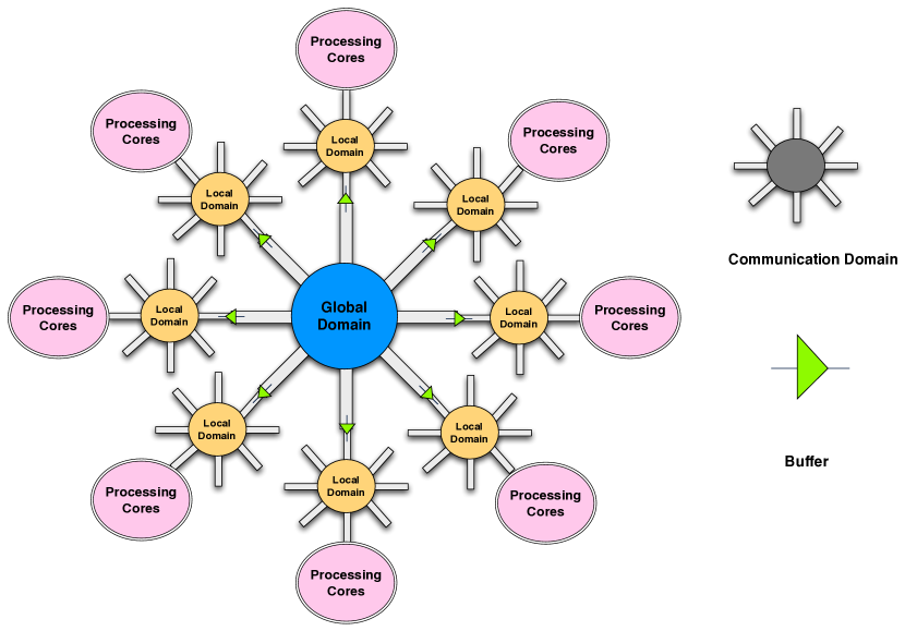
In this section we extend the local-communication network (targeting 32 cores) to the global-communication scale system that includes 1024 cores. In order to accommodate the performance and power requirements of the system, we leverage a hierarchical approach, depicted in Figure 5. This hierarchical approach reduces the total power the system needs and improves performance. This improvement is two fold: First, the optical power demand and bandwidth requirement is limited to number of nodes in the small network rather than whole thousand core, second, by isolating communication in different sub-networks in the hierarchy we can improve power and performance.
The system is divided into local and global communication domains. The thousand-core system is divided into 32-core domains, and each domain contains 32 cores in order to have a balanced number of nodes at both the global and local domains. A 32-core is considered a single local communication domain. This local domain is served by a single broadcast and linear network. The thousand-core chip system represents another communication domain which is called a global communication domain, where each local domain is considered to be a single node. The global domain is served by a second hierarchy of network. This additional hierarchical level is also composed of a broadcast and linear network. However, the power and performance requirements of the two communication domains differ. As shown in Figure 5, The the global domain (in blue) is connected through buffers to the local domains, while the local domains (in yellow) are connected to the cores (in pink).
The signal coming from one core to another core on another communication domain must pass through the local and global communication domains. First, at the local domain, there is a single access point to the global domain. At this access point the electrical signal/data is converted to the optical domain. The signal must travel from the source core to the global-local domain access-point. At the global-local domain access point, the signal undergoes an electro-optic conversion to regenerate the signal and buffer it, allowing it to travel the long distance across the thousand-core system. Next, the signal is carried in the global communication domain to the destination communication domain. At the destination communication domain, there is a single local-global domain access point to the core’s local communication domain. At this access point, the signal is re-generated and transmitted to the destination core.
The main difference between the local and global domain networks lies in bandwidth and traveling distance. In the global communication domain, the available area provides abundant space for space-division multiplexing. This area allows a myriad of parallel-running waveguides which, in turn, increases the bandwidth. Moreover, the area in the global domain is more (a factor of 32X), which permits the increase in bandwidth of the broadcast network since more waveguide-crossing can be accommodated. This increase in bandwidth of the broadcast and linear network at the global communication domain allows high concurrency and throughput which improves the performance of the whole system despite the large number of communicating nodes. As for the long traveling distance between communication domains, this leads to a quick increase in insertion loss. Hence, to compensate for this loss, we add electro-optic conversion points that regenerate the signal and allow it to travel a longer distance. In our system we need a single regeneration point in the broadcast network and eight regeneration points for the linear network in the global communication domain.
The full network including broadcast and linear network at the local and global- communication level are integrated with processing elements through 3D integration [35]. The network interface is connected to optical processing elements using TSV (through silicon via).
IV Flow control and system design
In this section we discuss the flow control of each sub-network of Hermes. We show how the broadcast network is leveraged for multicast operations, thanks to its global outreach. Meanwhile, the linear network serves as a point-to-point interconnect for long messages. These two sub-networks are connected hierarchically to serve the large-scale system which comprises a thousand cores. Moreover, we show how to improve locality at the system level to reduce global-communication and, at the local-communication level, to improve linear network operation.
IV-A Broadcast network flow control
The broadcast network has global outreach which enables it to serve multicast communication patterns. This kind of communication appears in cache coherence protocol messages and in arbitration. Next we discuss how this all-to-all broadcast network can be used for arbitration and communication in the system.
IV-A1 Bandwidth division
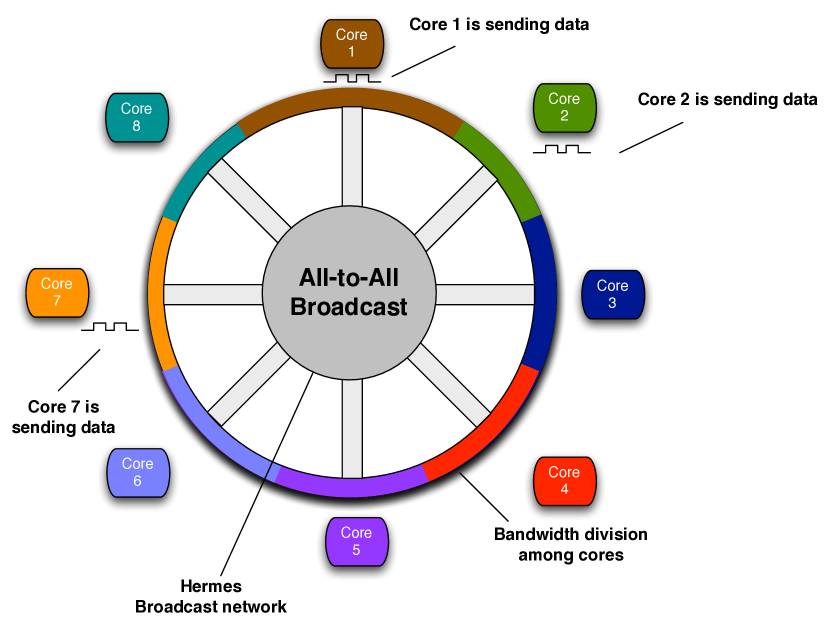
The designed network offers a plethora of bandwidth. This bandwidth needs to be shared efficiently and fairly between the communicating nodes. This section describes how the bandwidth is divided between the communicating nodes. Unlike earlier bandwidth division techniques, the presented approach herein is superior from two perspectives: First it exploits the full bandwidth dynamically and fairly even if contention is not 100%. Second, it utilizes the static laser power allocated to inactive nodes by sharing it among active communicating nodes.
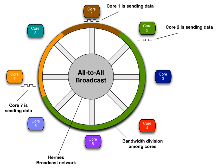
First, we consider a fair bandwidth division between nodes as shown in Figure 6. In this figure, the bandwidth is equally divided between communicating nodes. To improve bandwidth utilization we propose another scheme, this can be achieved by ordering the nodes in a circular closed set. Each node is assigned a dedicated fair-share bandwidth that it can use for broadcast. In addition, it uses the unused bandwidth of the next nodes in the ordered set until it encounters a node that is sending. Figure 7 shows the bandwidth division among eight nodes. In this setting, nodes one, two, and seven are sending on the network, while the rest of the nodes are idle. In this case, the bandwidth between node two and seven are free. Hence, node two can use this free bandwidth. Meanwhile, node seven has one neighboring idle node whose bandwidth can be used. This scheme allows efficient use of the overall bandwidth available to the network, which is 100%. Although bandwidth utilization is optimized across the network, fairness in bandwidth sharing is not guaranteed.
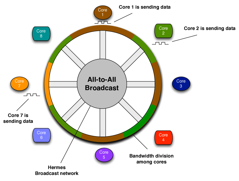
The scheme above has a high utilization of bandwidth but unfortunately its unfairness may lead to starvation. In order to improve the fairness of bandwidth sharing, we divide the nodes into groups. Each group can share the bandwidth as described above, but there is no cross-group sharing. Figure 8 shows an example of fair bandwidth-sharing, in this setting we have two groups which are group one including nodes one, three, five, and seven and group two including nodes two, four, six, and eight. In Group One node one and seven are sending while the rest are idle. The bandwidth of the nodes in this group is shared between the group members as described earlier. In this case, node one uses the bandwidth of nodes three and five. Meanwhile, node seven uses its bandwidth. In Group Two, core two uses all the bandwidth in this group. This mechanism allows more fair sharing of bandwidth but sacrifices some utilization efficiency of the bandwidth. This is because we may have groups with no nodes sending in it. Hence, there is a trade-off between fairness and utilization. To explain this, consider nodes and groups. In that case each group (which is a node) has a dedicated bandwidth. This achieves optimal fairness; however, since no two groups may share bandwidth, the utilization of bandwidth drops. On the other hand, when we have one group and nodes we have 100% utilization and low fairness. By adjusting the number of groups we can achieve a balance between fairness and utilization efficiency.
IV-A2 Arbitration for the broadcast medium
The broadcast network itself is a shared resource. In order to gain access to the network, communicating nodes need to arbitrate for this resource with other competing nodes and divide the bandwidth through a conflict resolution mechanism.
A node can gain access to the broadcast medium by signaling the other nodes a request for broadcast followed by sending data. For a -node network, we dedicate -wavelengths of the bandwidth for signaling a request to start a broadcast. At The next clock cycle, the requesting node may start broadcasting directly. Thus, this flow control approach introduces a single cycle overhead which is small. During the broadcast operation, the bandwidth is divided between nodes as described in Section IV-A1. By allowing several nodes to broadcast at the same time, we improve concurrency, latency, and fairness of the system.
Deadlock is not possible in the broadcast network since each node is given a minimum amount of bandwidth no matter how many nodes are contending for bandwidth. Moreover, the circuit-switching flow control inherit is silicon photonics guarantees no contention once access to the network is satisfied. Hence, deadlock will not occur in the broadcast network.
IV-A3 Arbitration for the linear network
Arbitration for the linear network is performed through the broadcast network. The procedure is a six phase process: (1) The requesting node checks a lookup table to determine that the path is clear. (2) The requesting node signals the rest of the nodes that a request for access has been made to the linear network. (3) The requesting node sends the destination node address. (4) All the nodes update their lookup table with the waveguide segments that are currently in use. (6) When the requesting node completes transmission, it brings down the request signal back to null indicating that it has completed the transaction. Thus, the rest of the nodes may update the lookup table to clear the segments that were reserved.
In order to guarantee fairness, a priority scheme is employed. Each node is given a random priority and access to the linear network is given to node with highest priority. This priority scheme shares the same seed; hence, no two nodes will share same priority at any given time. Moreover, the priority scheme changes periodically which avoids starvation situations. Moreover, this guarantees that deadlock will not occur during arbitration since every node will have a chance to get highest priority and gain access to the linear network. Once the node gains access to the linear network, the path is reserved and no cyclic wait over resources may occur. Hence, the network is deadlock free during arbitration and communication [3].
In order to support such flow control, several resources are needed. First, -wavelengths are dedicated to signal a request to access the linear network. Each of the -nodes has a globally known wavelength. Another important resource includes the lookup table. Each node is equipped with a lookup table to keep track of the waveguide segments that are used and those that are free. Thus, the lookup table frees the broadcast network from contention for reserved resources. Finally, to broadcast the destination address, each node consumes its dedicated bandwidth as explained in Section IV-A1.
IV-A4 Global order in broadcast network
In snoopy protocol, global ordering becomes crucial to guarantee the correctness of cache coherence protocol. Despite the fact that broadcast provides global ordering naturally; however, the hierarchical design and localization techniques (not all packets travel through the global domain) complicates the situation. Even within the local communication domain, the plethora of bandwidth allows multiple nodes to broadcast simultaneously. Hence, global ordering requires extra effort. In this design, each node is given a local order within its local domain. This order is random and changes periodically which avoids starvation. Moreover, since all nodes share same seed, collision will not occur. Packets sent are tagged by local order (5 bits). Packets received from different nodes are ordered by completion time, then by node local order. In case of packets arriving from global domain, these are sent by an intermediate node that receives packets from global domain and sends it to local domain. In this case, these packets take the order of the node that sends it. In the global domain, a similar scheme takes place where packets received are ordered by an order local to the global domain only [44].
IV-B System-level optimizations
At the system-level, the network design is hierarchical. Accessing the global communication domain from the local communication domain is done through an access point. All messages between these two domains goes through the access point which has a dedicated minimal bandwidth to avoid performance bottlenecks. Re-direction of messages to the global domain depends on the message type. For multicast messages, the access point will receive this message and using a bloom filter it will determine whether this message should go to the global domain or not, thus reducing the global domain traffic [45]. As for cache lines, which are point to point communication, re-direction depends whether the destination is on the same local-communication domain or not. If the destination is on another local-communication domain, the unicast cache line is re-directed to the global domain. Otherwise no re-direction occurs.
The cost of accessing the global communication domain is high in terms of power and latency. Hence, at the system-level our goal is to keep communication local. That is nodes that communicate often with each other are co-located in the same local communication domain. To achieve this goal communication localization techniques are leveraged. This includes workload migration [43] and data migration [42]. In this section we analytically formulate the thread-core assignment and page-core assignment in a binary integer programming problem. Then, we propose a greedy algorithm that gives near optimal results running at the kernel-level.
IV-B1 Problem formulation
The problem of assigning threads to cores to minimize communication in the global communication domain can be formulated as an binary integer programming problem. First, given threads and local-communication domain and a communication cost between thread and thread which is gathered from communication statistics per thread upon each kernel switch, we want to find an assignment of thread and thread to local-communication domain through workload migration. Then we assign the shared memory pages to the local-communication domain using data migration. is a binary variable which is one if thread and are in local-communication domain , while is an integer weight. Our optimization problem can be formulated as:
| (1) | ||||
| (2) | ||||
| (3) | ||||
| (4) |
where are the binary decision variables of size which determine which two threads are assigned to which local-communication domain. Equation 2 is a set of constraints that ensure each local-communication domain has exactly threads assigned to it where the number of constraints is , having one constraint per local-communication domain. Equation 3 is a set of constraints that ensure each thread is assigned with another threads to the same local-communication domain, where the number of constraints is , having one constraint per thread. Equation 4 ensures that each thread is assigned to one local-communication domain only, where the number of constraints is , having one constraint per 3-thread-tuple (for each thread, no thread pair occur in more than one local-communication domain).
The communication cost is computed as number of cache-lines exchanged between each pair of threads. This can be easily counted using a counter per thread. The kernel, periodically updates the communication cost for the whole system upon every context switch after which the communication counter needs to be reset. Finally, after assigning threads to cores through workload migration, the kernel assigns pages to local-communication domains through data migration [42].
IV-B2 Solution: Greedy algorithm
Solving the binary integer programming problem presented in Section IV-B1 is prohibitively expensive. It takes hours on a desktop for small core counts (16 to 36 cores). Not to mention that binary integer programming problems are NP-complete [46]. Hence, a more efficient approach is needed. For this purpose in our system, we propose a distributed greedy algorithm that re-assigns threads to cores. The algorithm is presented in Algorithm 1. First the function receive as the cost of communication between every pair of threads. Then it heapifies the matrix into a heap in a distributed manner [47]. Next, we iteratively extract the two clusters with highest communication and merge them in a greedy manner. Finally, we update the cost of communication of the different clusters with the new cluster in parallel using multiple kernel threads.
V Evaluation
In this section we evaluate the proposed design for a thousand-core system. Using a first-order analytic evaluation, we compare the proposed design with state- of-the-art solutions of silicon photonics scaled upto this a thousand-core system. First, we discuss the different networks we compare to in our simulations, and scale them hierarchically to a thousand-core system in a similar fashion to Hermes. Following this discussion, we present our performance results, then the power results including a discussion of how Hermes was able to achieve superior performance and power.
We analyze the power, latency, and bandwidth scalability of multicast mechanism for four classes of on-chip silicon photonic networks encompassing eight state-of-the-art different networks as shown in Table II. The first class is all-optical bus-based networks. This class includes networks that rely solely on optics for communication. More specifically, the broadcast networks in this class have a serpentine shape that reaches to all the cores (or core cluster). Examples of this class include Corona [6], ATAC [12] and Kirman’s bus-shaped architecture [48]. The second class of networks is hybrid networks that mix optical and electrical networks or routers such as Petracca et al. design [49] that leverages an electrical network. Other networks such as Joshi et al.’s Clos network [8] and Phastlane [10] leverage electrical routers and optical links. The third class of networks have a crossbar architecture where multiple nodes compete to send data to single receiver. In this network, the waveguide takes a serpentine shape reaching out to all nodes in the network. Examples of this class include Corona [6] and Flexishare [7]. The fourth and final class leverage antenna as a linear power division device for broadcast such as Iris [3].
V-A Power scalability
| Network | Bus | Hybrid | Crossbar | Antenna-based |
|---|---|---|---|---|
| Kirman Bus [48] | ||||
| ATAC [12] | ||||
| Flexishare [7] | ||||
| Corona [6] | ||||
| Phastlane [10] | ||||
| Clos [8] | ||||
| Columbia Mesh [49] | ||||
| Iris [3] |
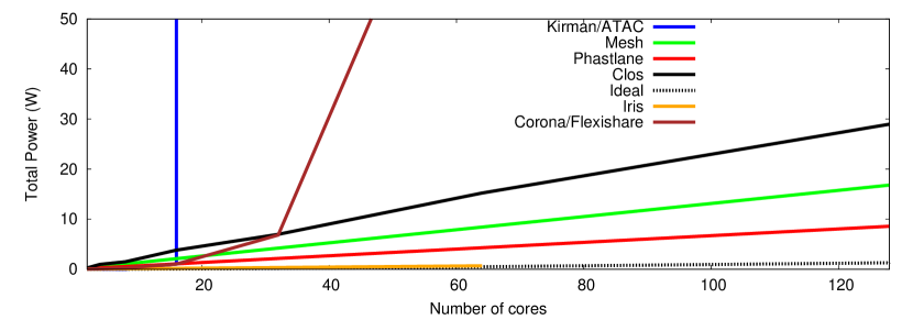
In this section we analyze the power scalability of the four classes of on-chip silicon photonic networks. In the first class of all-optical networks, that have serpentine-shaped topologies, these rely heavily on a broadcast network for arbitration and in some cases for cache coherence packets. The broadcast network is composed of a bus topology where each communicating node taps half the available power through a beam splitter. In this structure, half of the power goes to the core, and the other half continues onto the rest of the cores. Linear power division in bus-based broadcast, even though theoretically might be feasible, has not been demonstrated in the literature and their sensitivity to process variations remain unknown to our knowledge. Reliable and process-variation immune power splitters that are available in silicon photonics are 3 dB power splitters (50% splitting ratios) as we have shown in Section III-A. Moreover, to our knowledge, prior work assuming a photonic bus do not provide details about the device-level implementation of the bus-based architecture. The drawback of this topology is the exponential growth of optical power with numbers of cores (, where is number of cores). At a large number of cores, the power consumption of the broadcast network dominates and degrades the power efficiency of the overall system. As shown in Figure 9, the power levels of the network is acceptable for small networks. However, as the number of communicating nodes exceed sixteen, the power consumption increases dramatically as one can see in Bus in Figure 9. This makes the system unreliable since the majority of the power is converted to heat [50].
In the second class of networks, the hybrid optical-electrical solutions suffer from the high power consumption of the electrical components as one can see in Figure 9. Clos [8] has the highest power levels due to the high radix of its routers which greatly increases the power. Mesh by Columbia [49] has the second highest level because of the electrical links in addition to the routers in the electrical network. The overhead of electrical links have exceeded the power of buffered networks in Phastlane [10] despite its bufferless routers. Finally, Phastlane [10] has the lowest power due to the low radix routers and optical links. Despite the linear scaling trend of power (, where is number of cores) in this class of networks, the total power consumption is relatively high. As shown in Figure 9, the power levels of this class of networks is large — even for small networks. For a 32 node network, the electrical power can reach ten watts.
The third class of networks have a crossbar topology. In this class, the crossbar spans the whole cores in a serpentine-shaped topology. This serpentine shape has a high optical loss which increases exponentially with number of node, this can be explained as follow. Each node can send at any given time, hence, each node has its own power source. Moreover, the waveguide length increases with number of nodes but the length is longer than typical networks and can reach tens of centimeters. Assuming a 2.5 dB/cm [31] waveguide loss as we do assume for all other networks, then the total loss will increase exponentially with number of nodes (, where is number of cores).
The fourth and final class leverage an optical antenna for linear power division [36]. The main advantage of this approach is linear power division as shown in Figure 9. However, there are two drawbacks: First, optical antenna have poor power efficiency. The efficiency is as low as 23% [36] which limits the power efficiency of the statically allocated optical power in the whole system. Moreover, the number of ports in the antenna do not scale beyond 64 ports. Hence, the maximum system size is a 64-core system [3].
An ideal case is to have an optical network with linear power trends in the number of cores (, where is number of cores) like Iris [3] but with high optical efficiency. As we will show later, Hermes can achieve this goal. Hermes provides linear power division at an efficiency of 96%. This makes it superior to existing solutions and attractive for managing multicast communication in on-chip networks. Moreover, at large core count, and through hierarchical design the power is reduced to .
V-B Performance scalability
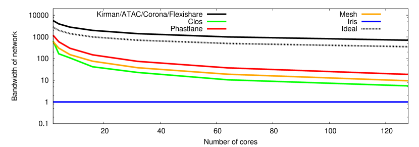
In this section we study the performance scalability of various networks. More specifically, we study how the bandwidth and latency of the broadcast network scales with the number of cores per chip. We define bandwidth as the bandwidth available for a core under zero load condition and 5 W power budget for the electrical components. On the other hand, we define latency as the worst case traversal time for a packet under zero load.
Figure 10 demonstrates the scalability of bandwidth for different designs. The first and third class represented in Kirman/ATAC/Corona/Flexishare in Figure 10 has a sub-linear decay in bandwidth per core (, where is number of cores). This returns to the constant chip area projected by ITRS [1] which limits the bandwidth per core. However, the bandwidth level are highest since the whole area is utilized for waveguides. The bandwidth in the second class is limited by the electrical power. As the bandwidth increases, the link and/or router power increase. Under the power constraint, the number of electrical components are greatly reduced and the trend is inversely proportional to the number of cores (, where is number of cores) as shown in the Figure 10. We can see that Phastlane [10] has more bandwidth than Mesh [49] which has more bandwidth than Clos [8]. This is because the available bandwidth scales inversely with the power consumption. Under a fixed power constraint low-power consuming networks can offer higher bandwidth levels. The fourth class of networks which is represented by Iris [3] has a constant bandwidth () and it is small due to the limitation on number of ports in the antenna. The bandwidth available in any clock cycle is 64 channels. Finally, the ideal case would follow the same trend of high bandwidth like class one and three (Bus and Crossbar). Hermes, shows high bandwidth that follows the same trend as class one and three but at a slightly lower bandwidth level.
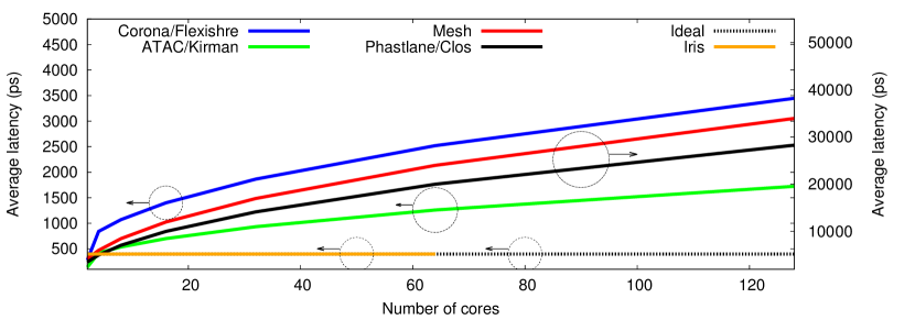
On the other hand, Figure 11 shows the scaling of latency of the broadcast network in different designs. Class one and three of networks have a high latency, linear in core-count (, where is number of cores), due to the serpentine shape of the broadcast network which has to pass through all nodes in the network serially. We can see that Corona [6] and Flexishare [7] exhibit higher latency than ATAC [12] and Kirman [48] since there is an arbitration cycle involved before sending the data. Class four, Iris [3], has constant and low latency, independent of the number of cores (), because the waveguide runs diagonally through the chip. This is the optimal case having lowest latency. However, Iris [3] does not scale beyond 64 cores due to the limitation of number of ports in the antenna. Class two (Mesh [49], Phastlane [10], and Clos [8]) has a sub-linear latency trend (, where is number of cores), but exhibits high latency levels due to the routing and switching overhead of the electrical routers. Mesh [49] has a lower latency because it leverages bufferless routers, meanwhile, Phastlane [10] and Clos [8] use buffered routers with higher delay. Finally, the ideal case should have low latency like Iris [3] but scalable to large core count. Hermes can offer this low latency and scale it to large core count. Moreover, through the use of hierarchical design, the latency is reduced to
VI Conclusion
In this study we have presented a novel broadcast-based network that can achieve linear power scalability with the number of nodes. Moreover, we have scaled the network to a hierarchical network that can serve a thousand-core chip system. First order power and performance evaluation of the proposed network show superior results compared to state-of-the-art silicon photonics networks. Moreover, communication locality have been greatly improved through kernel-level workload and data migration.
References
- [1] “International technology roadmap for semiconductors (ITRS),” 2009, http://www.itrs.net/Links/2009ITRS/Home2009.htm.
- [2] J. K. Ousterhout, et al., “The case for ramclouds: Scalable high-performance storage entirely in dram,” in SIGOPS OSR. Stanford InfoLab, 2009.
- [3] Z. Li, et al., “Global on-chip coordination at light speed,” IEEE Design and Test of Computers, vol. 27, pp. 54–67, 2010.
- [4] S. Beamer, et al., “Re-architecting dram memory systems with monolithically integrated silicon photonics,” in ISCA ’10: Proceedings of the 37th annual international symposium on Computer architecture. New York, NY, USA: ACM, 2010, pp. 129–140.
- [5] P. Koka, et al., “Silicon-photonic network architectures for scalable, power-efficient multi-chip systems,” in ISCA ’10: Proceedings of the 37th annual international symposium on Computer architecture. New York, NY, USA: ACM, 2010, pp. 117–128.
- [6] D. Vantrease, et al., “Corona: System implications of emerging nanophotonic technology,” in Proc. Int. Symp. Computer Architecture, 2008, pp. 153–164.
- [7] Y. Pan, J. Kim, and G. Memik, “Flexishare: Channel sharing for an energy-efficient nanophotonic crossbar,” in Proc. Int. Symp. High-Performance Computer Architecture, 2010, pp. 1–12.
- [8] A. Joshi, et al., “Silicon-photonic clos networks for global on-chip communication,” in Proc. Int. Symp. Networks-on-Chip, May 2009, pp. 124–133.
- [9] A. Shacham, K. Bergman, and L. Carloni, “Photonic networks-on-chip for future generations of chip multiprocessors,” Computers, IEEE Transactions on, vol. 57, no. 9, pp. 1246–1260, Sept. 2008.
- [10] M. J. Cianchetti, J. C. Kerekes, and D. H. Albonesi, “Phastlane: a rapid transit optical routing network,” in Proc. Int. Symp. Computer Architecture, June 2009, pp. 441–450.
- [11] N. Kirman, et al., “Leveraging optical technology in future bus-based chip multiprocessors,” in Proc. Int. Symp. Microarchitecture, 2006, pp. 492–503.
- [12] G. Kurian, et al., “Atac: a 1000-core cache-coherent processor with on-chip optical network,” in Proceedings of the 19th international conference on Parallel architectures and compilation techniques, ser. PACT ’10. New York, NY, USA: ACM, 2010, pp. 477–488.
- [13] S. Borkar, “Thousand core chips: a technology perspective,” in Proceedings of the 44th annual Design Automation Conference, ser. DAC ’07. New York, NY, USA: ACM, 2007, pp. 746–749. [Online]. Available: http://doi.acm.org/10.1145/1278480.1278667
- [14] D. Yeh, et al., “Thousand-core chips [roundtable],” Design Test of Computers, IEEE, vol. 25, no. 3, pp. 272 –278, may-june 2008.
- [15] Y. Pan, et al., “Firefly: illuminating future network-on-chip with nanophotonics,” in Proc. Int. Symp. Computer Architecture, June 2009, pp. 429–440.
- [16] N. E. Jerger, L.-S. Peh, and M. Lipasti, “Virtual circuit tree multicasting: A case for on-chip hardware multicast support,” in Proc. Int. Symp. Computer Architecture, June 2008.
- [17] A. Udipi, N. Muralimanohar, and R. Balasubramonian, “Towards scalable, energy-efficient, bus-based on-chip networks,” in High Performance Computer Architecture (HPCA), 2010 IEEE 16th International Symposium on, 2010, pp. 1 –12.
- [18] R. G. Beausoleil, et al., “Nanoelectronic and nanophotonic interconnect,” Proceedings of the IEEE, vol. 96(2), pp. 230–247, 2008.
- [19] S. Xiao, et al., “Low-loss ultra-compact soi microring add-drop filters,” in Frontiers in Optics. Optical Society of America, 2007, p. PDP_D6.
- [20] G. Reed, et al., “Silicon optical modulators,” Nature Photonics, vol. 4, no. 8, pp. 518–526, 2010. [Online]. Available: http://epubs.surrey.ac.uk/7096/4/licence.txt
- [21] G. Li, et al., “Ultralow-power high-performance si photonic transmitter,” in Optical Fiber Communication Conference. Optical Society of America, 2010, p. OMI2.
- [22] G. Li, et al., “25gb/s 1v-driving cmos ring modulator with integrated thermal tuning,” Opt. Express, vol. 19, no. 21, pp. 20 435–20 443, Oct 2011.
- [23] B. Lee, et al., “High-performance modulators and switches for silicon photonic networks-on-chip,” Selected Topics in Quantum Electronics, IEEE Journal of, vol. 16, no. 1, pp. 6 –22, jan.-feb. 2010.
- [24] X. Chen, et al., “Racetrack filters for nanophotonic on-chip networks,” in Integrated Photonics Research, Silicon and Nano Photonics Conference. Optical Society of America, July 2010, to be published.
- [25] L. Liu, et al., “Low-power electro-optical switch based on a iii-v microdisk cavity on a silicon-on-insulator circuit,” in Asia Communications and Photonics Conference and Exhibition. Optical Society of America, 2009, p. ThB2.
- [26] A. Biberman, et al., “Broadband silicon photonic electrooptic switch for photonic interconnection networks,” Photonics Technology Letters, IEEE, vol. 23, no. 8, pp. 504 –506, april15, 2011.
- [27] X. Zheng, et al., “A sub-picojoule-per-bit CMOS photonic receiver for densely integrated systems,” Opt. Express, vol. 18, no. 1, pp. 204–211, Jan. 2010.
- [28] J. Michel, J. Liu, and L. C. Kimerling, “High-performance ge-on-si photodetectors,” Nature Photonics, vol. 4, no. 8, pp. 527–534, 2010.
- [29] S. Liao, et al., “36 ghz submicron silicon waveguide germanium photodetector,” Opt. Express, vol. 19, no. 11, pp. 10 967–10 972, May 2011.
- [30] “Emtnano project,” 2008, http://http://www.colorado.edu/emtnano/home.
- [31] “ePIXfab,” http://www.epixfab.eu/.
- [32] L. Chen, et al., “Integrated GHz silicon photonic interconnect with micrometer-scale modulators and detectors,” Opt. Express, vol. 17, no. 17, pp. 15 248–15 256, Aug. 2009.
- [33] A. Alduino, et al., “Demonstration of a high speed 4-channel integrated silicon photonics wdm link with hybrid silicon lasers,” in Integrated Photonics Research, Silicon and Nanophotonics. Optical Society of America, 2010, p. PDIWI5.
- [34] X. Zheng, et al., “Ultra-efficient 10gb/s hybrid integrated silicon photonic transmitter and receiver,” Opt. Express, vol. 19, no. 6, pp. 5172–5186, Mar 2011.
- [35] B. Black, et al., “Die stacking (3d) microarchitecture,” in Proceedings of the 39th Annual IEEE/ACM International Symposium on Microarchitecture, ser. MICRO 39. Washington, DC, USA: IEEE Computer Society, 2006, pp. 469–479.
- [36] H. Zhou, et al., “On-chip wireless optical broadcast interconnection network,” Lightwave Technology, Journal of, vol. 28, no. 24, pp. 3569–3577, Dec. 2010.
- [37] X. Tang, et al., “A novel scheme for 1n optical power splitter,” Opt. Express, vol. 18, no. 21, pp. 21 697–21 704, Oct. 2010.
- [38] Y. Qian, et al., “Compact waveguide splitter networks,” Opt. Express, vol. 16, no. 7, pp. 4981–4990, Mar. 2008.
- [39] L. Cao, et al., “Adiabatic couplers in soi waveguides,” in Lasers and Electro-Optics (CLEO) and Quantum Electronics and Laser Science Conference (QELS), 2010 Conference on, may 2010, pp. 1 –2.
- [40] Y. Qian, et al., “Compact 90° trench-based splitter for silicon-on-insulator rib waveguides,” Opt. Express, vol. 15, no. 25, pp. 16 712–16 718, Dec. 2007.
- [41] M. Popovic, E. Ippen, and F. Kartner, “Low-loss bloch waves in open structures and highly compact, efficient si waveguide-crossing arrays,” Lasers and Electro-Optics Society.
- [42] C. Kim, D. Burger, and S. Keckler, “Nonuniform cache architectures for wire-delay dominated on-chip caches,” Micro, IEEE, vol. 23, no. 6, pp. 99 – 107, nov.-dec. 2003.
- [43] M. Lis, et al., “Brief announcement: distributed shared memory based on computation migration,” in Proceedings of the 23rd ACM symposium on Parallelism in algorithms and architectures, ser. SPAA ’11. New York, NY, USA: ACM, 2011, pp. 253–256. [Online]. Available: http://doi.acm.org/10.1145/1989493.1989530
- [44] N. Agarwal, L.-S. Peh, and N. Jha, “In-network snoop ordering (inso): Snoopy coherence on unordered interconnects,” in High Performance Computer Architecture, 2009. HPCA 2009. IEEE 15th International Symposium on, feb. 2009, pp. 67 –78.
- [45] A. Broder and M. Mitzenmacher, “Network applications of bloom filters : A survey,” Internet Mathematics, vol. 1, no. 4, pp. 485–509, 2004. [Online]. Available: http://akpeters.metapress.com/index/v7324576u920p665.pdf
- [46] M. R. Garey and D. S. Johnson, Computers and Intractability; A Guide to the Theory of NP-Completeness. New York, NY, USA: W. H. Freeman & Co., 1990.
- [47] M. A. A. A. hija, et al., “A heapify based parallel sorting algorithm.” Journal of Computer Science, vol. 4, no. 11, pp. 897 – 902, 2008.
- [48] N. Kirman, et al., “On-chip optical technology in future bus based multicore designs,” IEEE Micro, vol. 27(1), pp. 56–66, 2007.
- [49] M. Petracca, et al., “Design exploration of optical interconnection networks for chip multiprocessors,” in Proceedings of IEEE Symposium on High Performance Interconnects, 2008, pp. 31–40.
- [50] S. Abdollahi and M. K. Moravvej-Farshi, “Effects of heat induced by two-photon absorption and free-carrier absorption in silicon-on-insulator nanowaveguides operating as all-optical wavelength converters,” Appl. Opt., vol. 48, no. 13, pp. 2505–2514, 2009.