Planar Shielded-Loop Resonators
Abstract
The design and analysis of planar shielded-loop resonators for use in wireless non-radiative power transfer systems is presented. The difficulties associated with coaxial shielded-loop resonators for wireless power transfer are discussed and planar alternatives are proposed. The currents along these planar structures are analyzed and first-order design equations are presented in the form of a circuit model. In addition, the planar structures are simulated and fabricated. Planar shielded-loop resonators are compact and simple to fabricate. Moreover, they are well-suited for printed circuit board designs or integrated circuits.
Index Terms:
Electromagnetic induction, loop antenna, resonator, resonant inductive coupling, wireless power transmission.I Introduction

THE wireless transfer of electromagnetic energy provides an often indispensable convenience when physical interconnects are bulky, dangerous, or simply not feasible. Inductive coupling methods are attractive because they are safe, affordable, and simple to implement. However, the coupling is quasistatic, which inherently limits operation to the near field. In 2007, wireless non-radiative power transfer (WNPT) was demonstrated at mid-range distances using resonant inductive coupling [1]. Since that time, WNPT has received significant commercial interest and numerous applications have been pursued including the wireless powering of consumer electronics, electric vehicles [2] and implantable medical devices [3, 4, 5, 6]. WNPT has also been advanced and demonstrated by various research groups [7, 8, 9, 10, 11].
Coaxial, shielded-loop resonators were recently used as receiving and transmitting loops in a WNPT system [12, 13]. The fields generated by shielded-loop resonators are similar to those generated by classical resonators. However, these compact, self-resonant structures offer low losses, an input that is simple to feed, and confined electric fields, which could otherwise couple to nearby dielectric objects. A similar resonator was subsequently pursued in [14] for WNPT. An RLC circuit model was derived for these loops in [13] using the properties of the coaxial transmission line from which they are constructed. Aside from power transfer, these resonant loops could be used for near-field communication [15, 16]. Non-resonant versions have been used for magnetic-field probing [17, 18].
The loops in [13, 14] were fabricated using lengths of semirigid coaxial transmission line. However, these types of loops can be difficult to fabricate. Moreover, their fabrication may not be repeatable. A planar structure made from a printed circuit board (PCB) would not only be simpler to fabricate but would also allow transmission-line properties, such as the characteristic impedance, , to be tailored. These resonators could be used to wirelessly power single chips [19] or 3-D integrated circuits [20, 13, 21]. The demand for chip real estate makes these compact, planar shielded-loop resonators advantageous. Planar shielded-loop resonators make economical use of space, since the inductance and capacitance are formed using the same conductive loops. This need for compact WNPT structures in practical systems is often stressed in literature [22, 23, 24].
In this paper, planar stripline and microstrip loop resonators are proposed and analyzed. In coaxial shielded loops, currents exist on the interior and exterior of the outer conductor, separated by the skin effect [12, 13]. However, this paper shows that such separation is not required. Equations for characteristic impedance , conductor attenuation , and dielectric attenuation [25, 26, 27] are used to develop first-order mathematical models for the stripline and microstrip resonators. The models are compared to both full-wave simulation and measurement. The trends of efficiency versus loop parameters are explored and compared for the different structures. The effect of re-positioning the slit in the ground conductor of the shielded planar loops is also explored.
II Background
Planar shielded-loop resonators behave in much the same way as their coaxial counterparts. Therefore, coaxial shielded loops are reviewed before introducing planar shielded-loop resonators. In addition, re-positioning the slit in the ground conductor is discussed.
II-A Coaxial Shielded-Loop Resonators
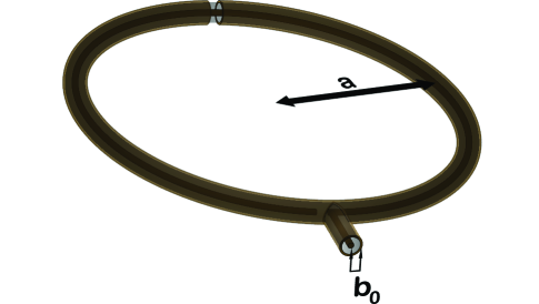
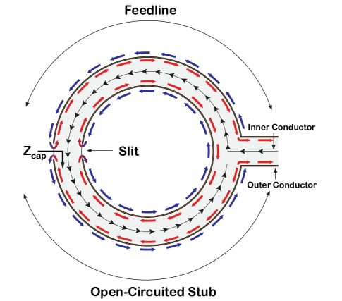
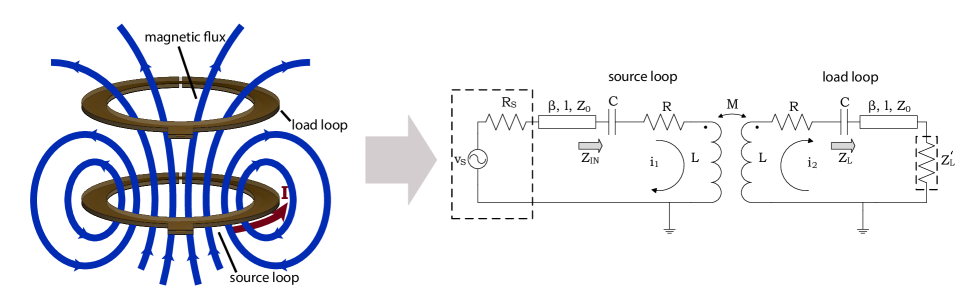
Figure 1(a) shows a shielded-loop resonator constructed from a loop of coaxial transmission line with circular cross section. The outer conductor is continuous except for a small slit halfway around the loop. Figure 2 shows the behavior of the current on a coaxial shielded-loop resonator. The current enters the input of the loop and propagates along the interior of the coaxial line to the slit in the outer ground conductor. It then wraps around the exterior of the loop to the opposite end of the slit, returning to the interior and ending at the open-circuited stub. The current does not traverse the slit directly due to the high reactance presented by the gap. As a result, the width of the slit does not appreciably affect the resonant frequency. If the outer conductor is thick (several skin depths), a current propagating on the interior of the outer conductor will be isolated from the current propagating on its exterior. This results in a loop current (inductor) in series with the open-circuited stub. The stub can be modeled as a capacitor for electrical lengths less than a quarter-wavelength (). Two magnetically-coupled, symmetric, coaxial shielded-loop resonators are modeled by the circuit shown in Fig. 3. The circuit includes the feedline, which precedes the slit. The feedline transmission line is characterized by a propagation constant , a physical length , and a characteristic impedance . The parasitic resistance represents conductor, dielectric, and radiative losses. The input source is represented by input voltage and input impedance .
II-B Circuit Model for Shielded Loops
As discussed in [13], shielded-loop resonators can be modeled as RLC resonators. For a coaxial cross section, the inductance of the loop can be approximated using the following well-known equation [28]:
| (1) |
Here, is the mean radius of the loop and is the radius of the conductor cross section. For an electrically-small stub of length (), the impedance looking into the open-circuited stub is:
| (2) |
Therefore, the capacitance of the stub is simply:
| (3) |
Here, is the per-unit-length capacitance of the transmission line. From and , the resonant frequency can be determined:
| (4) |
The resistance accounts for four loss mechanisms: radiative loss, exterior conductor loss, equivalent series resistance (ESR) of the capacitor, and feedline loss. The resistances representing these losses are given by the following expressions [14]:
| (5) | ||||
| (6) | ||||
| (7) | ||||
| (8) |
where is the free-space wavelength at the frequency of operation, is the complex propagation constant of the transmission line, is the per-unit-length resistance of the transmission line, and is the outer conductor perimeter for a cross-sectional slice of the loop. For the coaxial shielded-loop resonator shown in Figure 1(a), . The complex propagation constant is defined as in [25]:
| (9) |
where and are the per-unit-length dielectric conductance and per-unit-length inductance, respectively. For the circuit model in Figure 3, the feedline loss is included in and the propagation constant is purely real ().
In (6), a uniformly-distributed surface current is assumed, while (8) assumes that the feedline is half the circumference of the loop. For electrically-small loops, can be simplified to:
| (10) |
The term in (7) and (10) results from the length of the open-circuited stub being half the loop circumference.
Knowing the transmission-line properties (, , , ), the external geometry of the structure, and the resonant frequency using (4), the of the resonator can be determined:
| (11) |
These equations can also be applied to loop resonators made from planar transmission lines, which will be discussed next. However, these equations are only an approximation. A more accurate extraction of the resonator parameters can be performed through full-wave simulation. In this paper, equations (1) through (11) are referred to as the first-order design equations. For the planar loop resonators presented in Section III, another equation is added to relate the width of a planar cross section to the radius of a coaxial cross section.
II-C Location of the Ground Slit
The shielded-loop resonators used previously for wireless non-radiative power transfer employed a slit halfway around the loop [12], as shown in Fig. 1(a). For shielded-loops used in field probing, this location is chosen to minimize the probe’s response to the electric field [17, 18]. However, this is of less concern for wireless power transfer applications. Furthermore, the arguments made thus far to justify the operation of these planar structures did not stipulate a specified location for the slit. Therefore, a structure with a slit 10° from input (see Fig. 1(b)) will be introduced. Reducing the length of the feedline is advantageous, since this improves the performance of the loop over a broad frequency range (see Appendix A).
III Planar Shielded-Loop Resonators
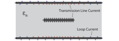
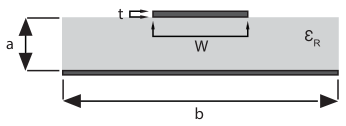
Coaxial, shielded-loop resonators (see Fig. 1(a)) can be difficult to fabricate, especially with repeatability. A planar structure, like that shown in Figure 1(b), made from a printed circuit board is simpler to fabricate and allows tailoring of transmission-line properties, such as the characteristic impedance . The cross section of a planar shielded-loop resonator made from a shielded stripline is shown in Fig. 4(a). To fabricate this structure, a loop can be cut from a PCB and its edges plated. Without plating, the dielectric on the edges of the loop is exposed, as shown in Figure 4(b), and the currents on the interior and exterior of the ground conductor are no longer physically isolated.
In Section II, the behavior of the coaxial shielded-loop resonator was explained by the physical separation of the currents on the ground conductor. However, simulation shows that a stripline loop resonator behaves similarly whether it is shielded or not (Fig. 4(a) and 4(b), respectively). For unshielded structures, the loop current on the ground conductor naturally separates from the transmission-line current, as shown in Fig. 4(b). Therefore, these currents can be treated separately as a transmission-line current and a loop current. It will be shown that there are only minor differences in the extracted resonator parameters for loops having cross sections corresponding to Fig. 4(a) or Fig. 4(b).
The cross section for an alternative loop resonator using a microstrip transmission line is shown in Fig. 5. With only two metal layers, this structure is simpler to fabricate but is not shielded.
Analytically characterizing these planar structures is challenging. For example, the inductance is not solely due to the outer loop current, since the transmission line itself contributes to the overall inductance. However, a first-order approximation can be made with some simplifying assumptions. In particular, let’s assume that the loop current flows uniformly on the exterior of the ground conductor. The formulas for resistive loss then become significantly simpler. The capacitance from the open-circuited stub can be easily approximated using (3). Assuming that the transmission line does not contribute to the total loop inductance, the inductance of a thin annulus can be used. This paper uses the following relationship:
| (12) |
where is the radius of the conductor cross section in equation (1) and is the width of planar cross section in the planar structure (see Fig. 4(a)). This relationship between round wires and strips can be found in [29]. For each type of loop resonator, the properties of the transmission line and the geometry of the loop are all that are needed for this first-order analysis.
IV Analytical Modeling
In Section II, the theory governing shielded-loop resonators was presented along with a corresponding RLC model. To determine the values of , , and , the geometry and transmission-line properties of the resonators must be used. Therefore, design equations for both stripline and microstrip transmission lines are presented in this section. The resulting models will be subsequently compared to both simulation and experiment.
IV-A Useful Transmission-Line Equations
In this paper, Wheeler’s formulas are used to compute the characteristic impedance of a centered stripline [26]. The formulas from Hammerstad and Jensen are used to calculate the characteristic impedance of a microstrip transmission line [27].
The equations for can also be used to calculate , , , and . Indeed, the conductor attenuation is computed using Wheeler’s incremental inductance rule, which is valid for any type of transmission line [25]:
| (13) |
where refers to the distance by which the walls of the conductors recede (see [25]) and is the sheet resistance of the conducting surfaces, which can be derived from the frequency and conductivity [25]:
| (14) |
Equation (14) assumes a uniform current distribution on the conductor’s surface. However, due to the proximity effect this is only an approximation [30]. Therefore, the conductor attenuation will be slightly higher than predicted by (13).
The dielectric attenuation is computed using the following formula presented in [25], which is also valid for any type of transmission line:
| (15) |
The per-unit-length resistance and conductance are also needed. From [31], these can be computed for a transmission line using and , respectively:
| (16a) | ||||
| (16b) | ||||
The per-unit-length capacitance and inductance are required as well. Since the transmission-line fields are quasi TEM:
| (17a) | ||||
| (17b) | ||||
| (17c) | ||||
Here, is the phase velocity of the wave and is the effective permittivity of the transmission line. For stripline, , where is the relative permittivity of the dielectric.
Using , , , , and for the various geometries, the values of , , and for the circuit model (see Figure 3) are calculated. The resulting and resonant frequency for each geometry is compared to those extracted from full-wave simulation.
V Stripline Loop Resonators
Stripline shielded-loop resonators are simulated using the commercial electromagnetic solver Ansys HFSS. To extract the resonator , , and parameters, the S-parameters are de-embedded to the location of the slit. Then, the de-embedded input impedances are used to extract the RLC parameters.
V-A Extraction Example
To demonstrate the RLC extraction procedure for these structures, an example is provided here for a stripline shielded-loop resonators with an inner conductor width = 10 mm. From the full wave simulation, the characteristic impedance and electrical length of the feedline is found to be 17.6 and 17.8° respectively, at 30 MHz. Using these numbers, the simulated input impedance versus frequency is de-embedded to the location of the slit by first converting to S-parameters and applying a frequency-dependent phase shift:
| (18) | ||||
| (19) |
Here, denotes the de-embedded S-parameters, is in MHz, and = 17.6 . The de-embedded input impedance is given as:
| (20) |
The resonant frequency is given by the frequency at which . The input reactances at two distinct frequencies near is used to determine and . The resonator resistance is simply the real part of the input impedance at resonance. The RLC parameters for the selected example are provided in Table I.
V-B Shielded Stripline Resonator
First, a set of shielded, stripline resonators with varying inner conductor widths are simulated to test the model presented in Section II. Referring to the cross section in Fig. 4(a), the properties of the simulated loop were:
-
•
Conductor: copper ( = S/m)
-
•
Dielectric: Rogers RT/Duroid 5880
-
•
: 2.2
-
•
: 0.009
-
•
Copper thickness (): 70 m
-
•
Loop radius (): cm
-
•
Cross-sectional width (): mm
-
•
Cross-sectional thickness (): mm
| 2 mm | 54.7 | 0.400 | 21.2 | 0.532 | 258 |
| 3 mm | 49.1 | 0.379 | 27.7 | 0.394 | 297 |
| 4 mm | 44.9 | 0.376 | 33.5 | 0.325 | 325 |
| 5 mm | 41.7 | 0.367 | 39.7 | 0.279 | 345 |
| 6 mm | 39.2 | 0.357 | 46.4 | 0.240 | 365 |
| 7 mm | 37.0 | 0.350 | 52.9 | 0.215 | 378 |
| 8 mm | 35.2 | 0.342 | 59.9 | 0.195 | 388 |
| 9 mm | 33.6 | 0.344 | 65.5 | 0.183 | 396 |
| 10 mm | 32.2 | 0.337 | 72.6 | 0.166 | 410 |
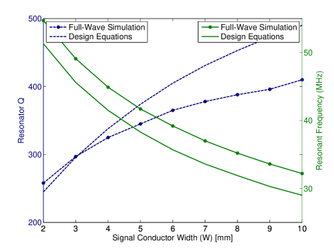
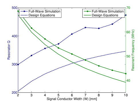
From the extracted data, shown in Table I, a few observations can be made. The resistance of the resonator decreases with increasing signal trace width . Narrower widths exhibit higher loss due to increased current densities. Loop inductance also decreases with increasing signal width . This is because the transmission line contributes to the overall inductance of the structure. This contribution decreases with increasing width . Such a phenomenon can be seen even from (1), where the inductance of a loop of coaxial cross section decreases with increasing cross-sectional radius.
Figure 6 shows the resonant frequency and Q factor extracted from full-wave simulation compared with those computed using the first-order design equations presented in Section II. The computed resonant frequencies match fairly well with simulation and the Q factors exhibit the proper trend. The design equations generally overestimate the Q factor.
V-C Unshielded Stripline Resonator
Next, a set of unshielded, stripline resonators (see Fig. 4(b)) with varying inner conductor widths are simulated. The geometry and material properties are the same as for the plated case, but without metal plating on the edges.
| 2 mm | 54.5 | 0.406 | 21.0 | 0.527 | 264 |
| 3 mm | 49.1 | 0.381 | 27.6 | 0.381 | 308 |
| 4 mm | 45.0 | 0.372 | 33.6 | 0.343 | 307 |
| 5 mm | 41.8 | 0.362 | 40.0 | 0.264 | 360 |
| 6 mm | 39.2 | 0.357 | 46.0 | 0.231 | 382 |
| 7 mm | 37.1 | 0.353 | 52.2 | 0.205 | 401 |
| 8 mm | 35.3 | 0.344 | 59.3 | 0.183 | 415 |
| 9 mm | 33.7 | 0.338 | 66.1 | 0.168 | 427 |
| 10 mm | 32.3 | 0.336 | 72.2 | 0.155 | 440 |
From Table II, the extracted resonator parameters for the unplated, stripline resonators are essentially the same as for the shielded-stripline resonators. However, the resistances of the unplated loops are slightly higher than for the plated loops. This occurs because the current is more spread out on the plated loop. Thus, plating the loops lowers the resistance but also adds a fabrication step.
V-D Shielded-Stripline Resonator with Shifted Slit
As mentioned in Section II, the slit in the ground conductor need not be placed opposite the input. Moving the slit toward the input feedline simply increases the length of the capacitive stub section. In addition, it decreases the length of the input feedline, which does not contribute to either the structure’s overall inductance or capacitance, and can adversely affect the efficiency of a WNPT system (see Appendix A). Therefore, structures are also simulated for loops with the slit in the ground conductor 10° from the input feedline (see Fig. 1(b)). All other dimensions are the same as before. The extracted data is given in Table III. From Table III, the capacitance of the structure doubles, while the inductance remains roughly the same. Furthermore, the resistance of the structure decreases. Although the frequencies are lower, the Q of the structure at resonance is slightly larger due to the reduced loss.
| 2 mm | 37.8 | 0.416 | 42.5 | 0.388 | 255 |
| 3 mm | 34.0 | 0.396 | 55.4 | 0.302 | 280 |
| 4 mm | 31.2 | 0.386 | 67.5 | 0.255 | 296 |
| 5 mm | 29.0 | 0.368 | 81.8 | 0.219 | 306 |
| 6 mm | 27.3 | 0.360 | 94.5 | 0.194 | 319 |
| 7 mm | 25.8 | 0.351 | 108.5 | 0.175 | 326 |
| 8 mm | 24.5 | 0.348 | 121.1 | 0.164 | 327 |
| 9 mm | 23.5 | 0.338 | 136.2 | 0.147 | 339 |
| 10 mm | 22.5 | 0.335 | 149.0 | 0.139 | 343 |
V-E Experimental Results
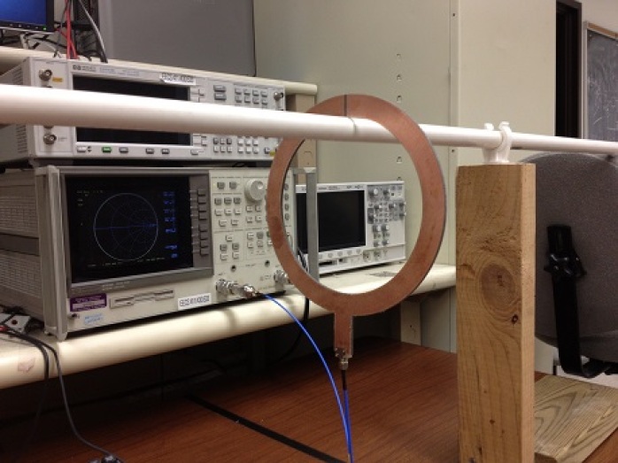
Unplated stripline loops with a ground slit opposite the input were fabricated to compare with the simulation and the analytical model. Two Rogers RT/Duroid 5880 substrates were etched, bonded together using FR406 no-flow prepreg, and cut to form the loops. Figure 7 shows the fabricated stripline loop resonator. The dimensions of the loop are the same as that for the loop described by Table II. A trace width = 10 mm is used. The simulation and experimental results for this loop are shown in Table IV.
| Simulation | 32.3 | 0.336 | 72.2 | 0.16 | 440 |
| Measurement | 32.1 | 0.326 | 75.4 | 0.20 | 348 |
| Model | 29.0 | 0.364 | 82.5 | 0.14 | 490 |
VI Microstrip Loop Resonators
Microstrip loop resonators are simulated using the commercial electromagnetic solver HFSS. The resonator parameters , , and are determined using the methods presented in Section IV.
VI-A Simulation Results
A set of planar, microstrip loop resonators with varying signal conductor widths are simulated to compare to the stripline loop resonators. The same dielectric and conductor as before are used. Referring to Fig. 5, the other properties of the loop were:
-
•
: cm
-
•
Cross-sectional width (): mm
-
•
Cross-sectional thickness (): mm
| 2 mm | 68.6 | 0.414 | 13.0 | 0.598 | 299 |
| 3 mm | 61.6 | 0.409 | 16.4 | 0.477 | 331 |
| 4 mm | 57.1 | 0.391 | 19.9 | 0.394 | 356 |
| 5 mm | 53.4 | 0.381 | 23.4 | 0.343 | 372 |
| 6 mm | 50.9 | 0.372 | 26.4 | 0.291 | 407 |
| 7 mm | 48.4 | 0.362 | 29.8 | 0.256 | 430 |
| 8 mm | 46.0 | 0.367 | 32.6 | 0.248 | 427 |
| 9 mm | 44.2 | 0.364 | 35.6 | 0.229 | 442 |
| 10 mm | 42.8 | 0.358 | 38.7 | 0.203 | 474 |
From Table V, it can be seen that the capacitance of the microstrip structure is lower than for the stripline structure. This follows from the decreased per-unit-length capacitance of the microstrip transmission line. The total inductance is increased because the height of the structure is decreased and the current on the ground conductor is more confined.
The resistance of the structure is lower compared to the stripline structure at similar frequencies. This is due to the fact that the fields partially exist in the air above the substrate, resulting in lower dielectric loss. However, this also means that the effective permittivity of the structure can be affected by objects in air directly above the substrate. Thus, the capacitance of the overall structure can be altered, which will detune the resonator. This is one disadvantage of the microstrip structure. On the other hand, fewer conductor layers are required and losses are lower.
Figure 8 shows the resonant frequency and Q factor extracted from full-wave simulation compared with those computed using the first-order model in Section II. Again, the computed resonant frequencies match fairly well, and the Q factors exhibit the proper trend. The design equations, however, underestimate the Q factor.
VI-B Microstrip Resonator with Shifted Slit
| 2 mm | 46.4 | 0.443 | 26.5 | 0.369 | 350 |
| 3 mm | 42.4 | 0.431 | 32.7 | 0.289 | 398 |
| 4 mm | 39.3 | 0.421 | 39.0 | 0.267 | 389 |
| 5 mm | 36.9 | 0.407 | 45.8 | 0.234 | 403 |
| 6 mm | 34.8 | 0.408 | 51.3 | 0.219 | 407 |
| 7 mm | 32.9 | 0.401 | 58.2 | 0.209 | 398 |
| 8 mm | 31.5 | 0.377 | 67.6 | 0.185 | 403 |
| 9 mm | 30.3 | 0.384 | 71.8 | 0.179 | 409 |
| 10 mm | 29.3 | 0.375 | 79.0 | 0.167 | 412 |
As with the stripline structures, a microstrip loop resonator with the ground slit shifted 10° from the feed is also simulated. The extracted resonator parameters are shown in Table VI. As before, the capacitances double while the inductances remain roughly the same. The Q factor of these resonators are similar to the original microstrip resonators described in the previous section, despite the lower frequencies.
VI-C Comparison with Lumped Matching
| 42.4 | 0.469 | 30 | 0.244 | 512 |
Here, the performance of the non-shifted microstrip loop resonator of width = 10 mm is compared to the traditional lumped topology. To this end, an inductive loop is simulated using the commercial electromagnetic solver Ansys HFSS. The loop had radius = 9 cm and width 20 mm. The resulting inductance is = .469 H and the parasitic resistance is = 0.184 . To match the resonant frequency = 42.9 MHz to that of the microstrip resonator, a 30 pF lumped capacitor is selected from Murata with equivalent series resistance of 0.06 . The result is an RLC resonator with characteristics given in Table VII.
Although the Q and inductance of the lumped system is higher, achievable resonant frequencies are limited by by the availability of lumped capacitors. Moreover, the lumped capacitors limit the power-handling capabilities of the system.
VI-D Experimental Results
| Simulation | 42.8 | 0.358 | 38.7 | 0.20 | 474 |
| Measurement | 42.1 | 0.347 | 41.3 | 0.24 | 381 |
| Model | 39.2 | 0.364 | 45.3 | 0.26 | 346 |
Microstrip loops with a ground slit opposite the input were fabricated to compare with simulations and the analytical model. The loops were milled and cut from a Rogers RT/Duroid 5880 substrate. The dimensions of the loop are the same as that for the loop described by Table V. A trace width = 10 mm is used. The simulation and experimental results for this loop are shown in Table VIII.
VI-E Bandwidth
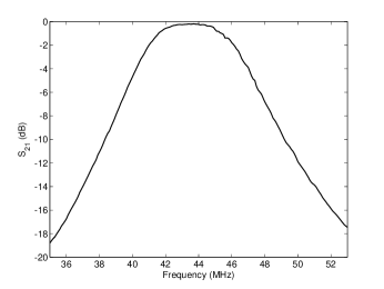
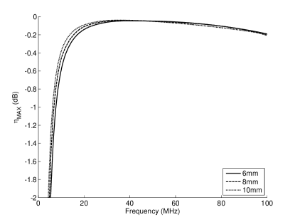
To explore the bandwidth of a system of coupled loops, the S-parameters of two microstrip loop resonators ( mm) separated by cm are measured. The power transfer efficiency is plotted in Figure 9 assuming an impedance match at MHz using an ideal L-matching network. The system achieves a power transfer efficiency of 96% and a 3-dB bandwidth of 6 MHz. Since wireless power transfer systems typically employ continuous waves, this bandwidth is sufficient.
VII Conclusion
This paper introduced planar alternatives to coaxial shielded-loop resonators with a circular cross section, used previously for wireless non-radiative power transfer (WNPT). It was shown that physically shielding the transmission-line current from the inductive loop current is not required to maintain the resonant behavior of the structure. Therefore, the stripline loops’ edges need not be plated. Structures with varying conductor widths were analyzed and simulated. Increased widths lowered both loss and the resonant frequency. For the same signal trace width , the microstrip loops exhibited higher Q values than the stripline loops. Structures were fabricated and their measured values matched well with simulation.
These planar shielded loops offer a number of advantages over earlier resonant loops. First, the structures are inherently suitable for printed circuit boards and integrated circuits, since they are planar. Second, the structures are physically compact. Essentially, these structures are capacitors made from a pair of conductive annuli onto which a loop current (inductance) has been impressed. Third, the widths of the signal conductor can be easily varied to manipulate the loop parameters, such as the characteristic impedance. Fourth, the power-handling capabilites are superior to a simple loop with a lumped series capacitor. Finally, the fabrication variance for the capacitance of the structure is lower than that of a lumped series capacitor.
It was also shown in simulation that the location of the slit in the ground conductor of the proposed loops need not be directly opposite the input feedline. Instead, its location can be used to vary the capacitance and therefore the resonant frequency of the resonators. Moreover, a significant length of feedline can adversely affect the performance of the WNPT system (see Appendix A).
Future research directions include the use of air as a dielectric to create higher-Q loop resonators for wireless non-radiative power transfer. The dielectric loss tangent is a significant contributor to the parasitic loss of the structure, so an air dielectric would be advantageous. Other research directions include using an array of these planar structures to manipulate the near-field in an attempt to enhance mutual coupling between source and receiving loops.
Appendix A Effect of Feedline on Power Transfer Efficiency
A-A Effective Resistance of the Feedline


Consider an RLC resonator with a length of lossy transmission line attached to the input (see Figure 10(a)), representative of a shielded-loop resonator. The transmission line can be decomposed into a lossless transmission line and an effective series resistance (see Figure 10(b)). The resistance can be determined by calculating the power dissipated in the feedline and dividing it by (defined in Figure 10(b)):
| (21) |
It can be shown that the effective resistance will reach a minimum at a frequency near the resonance of the RLC circuit. The effective resistance will increase as the excitation frequency is moved away from this minimum. This effect becomes more pronounced with longer transmission lines. For two magnetically-coupled RLC circuits (loops), the result is a decrease in maximum power transfer efficiency. This follows directly from the general equation for power transfer efficiency of the symmetric, coupled-loop system shown in Figure 3 [32]:
| (22) | |||
where is the power reflection coefficient, which depends on the impedance mismatch at the source, and . Clearly, if increases, the efficiency of the system decreases. For loops that use a feedline, contributes to the total .
To derive an expression for as a function of frequency, let’s write an expression for the power lost in the feedline:
| (23) |
From the equation for the impedance looking into a transmission line:
| (24a) | ||||
| (24b) | ||||
Here, is the complex propagation constant of the transmission line, where quantifies the attenuation along the line. Using (24a) and (24b):
| (25a) | ||||
| (25b) | ||||
Here, is defined as:
| (26) | ||||
The impedance , the characteristic impedance , and the function have been decomposed into their real and imaginary parts so that , , and .
The power dissipated in the feedline can be written as:
| (27) |
Using (27), the effective resistance can be written as:
| (28) |
The current can be written in terms of using the Z-matrix of the transmission line:
| (29) |
Substituting (25a), (26), and (29) into (28) provides an equation for as a function of , , line length , and . Under the assumptions , , and , the equation simplifies to:
| (30) |
By taking the derivative of (30), it can be shown that for a given frequency and transmission line, achieves a minimum when :
| (31) |
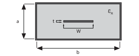
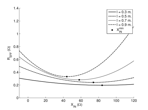
Figure (11) shows the variation of with using (30) for a microstrip line of varying lengths attached to a lossless, reactive load . The minima given by (31) are also plotted. The parameters of the microstrip, referring to Figure 5, are as follows:
-
•
Height (a) = 813 m
-
•
Width (W) = 2 mm
-
•
Relative Permittivity () = 3.0
-
•
Conductivity () = 5.8e7 S/m
-
•
Conductor Thickness (t) = 35 m
-
•
Loss Tangent () = 0.001
The values of and are extracted from the commercial circuit solver ADS at 40 MHz:
From Figure 11, a longer feedline exhibits a higher and a lower .
To verify (30), the analytical for the equivalent circuit of Figure 10(b) is compared with the simulated for the actual circuit of Figure 10(a).
A-B Implications for Coupled Loops
Referring to Figure 3, the input impedance for a symmetric system of magnetically-coupled loops in a WNPT system can be written as [13]:
| (32) |
For maximum power transfer [13]:
| (33) |
Using the same analysis as for a single loop, will be minimized at a point . As a result, the maximum achievable power transfer efficiency decreases as increases in the presence of an input feedline.
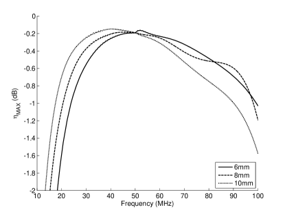
To verify these conclusions, pairs of coupled shielded-loop resonators from Tables I and III are simulated at a coupling distance of 10 cm. The maximum power transfer efficiency (achievable under a simultaneous conjugate match at both ports) is plotted versus frequency using the simulated S-parameters. Although thus far only the behavior of with respect to has been discussed, the behavior versus frequency is similar. Figure 12(a) shows the maximum power transfer efficiency for three different systems of coupled shielded-stripline loop resonators like those presented in Table I. Three different trace widths are used for the loops. It is clear that the efficiency is reduced for the higher frequencies. Figure 12(b) shows the same results for the loops characterized in Table III (shifted ground slit). The plots demonstrate that reducing the length of the feedline improves the performance of the loops away from the frequency corresponding to the minimum .
Acknowledgment
This work was supported by a Presidential Early Career Award for Scientists and Engineers (FA9550-09-1-0696).
References
- [1] A. Kurs, A. Karalis, R. Moffatt, J. D. Joannopoulos, P. Fisher, and M. Soljačić, “Wireless power transfer via strongly coupled magnetic resonances,” Science, vol. 317, no. 5834, pp. 83–86, 2007.
- [2] T. Imura, H. Okabe, and Y. Hori, “Basic experimental study on helical antennas of wireless power transfer for electric vehicles by using magnetic resonant couplings,” in 2009 IEEE Vehicle Power and Propulsion Conference, September 2009, pp. 936–940.
- [3] K. Jung, Y.-H. Kim, E. J. Choi, H. J. Kim, and Y.-J. Kim, “Wireless power transmission for implantable devices using inductive component of closed-magnetic circuit structure,” in 2008 IEEE International Conference on Multisensor Fusion and Integration for Intelligent Systems, August 2008, pp. 272–277.
- [4] Y.-X. Guo, D. Zhu, and R. Jegadeesan, “Inductive wireless power transmission for implantable devices,” in 2011 International Workshop on Antenna Technology (iWAT), March 2011, pp. 445–448.
- [5] C. Koch, W. Mokwa, M. Goertz, and P. Walter, “First results of a study on a completely implanted retinal prosthesis in blind humans,” in 2008 IEEE Sensors, October 2008, pp. 1237–1240.
- [6] F. Zhang, X. Liu, S. Hackworth, R. Sclabassi, and M. Sun, “Wireless energy delivery and data communication for biomedical sensors and implantable devices,” in 2009 IEEE 35th Annual Northeast Bioengineering Conference, April 2009, pp. 1–2.
- [7] A. Sample, D. Meyer, and J. Smith, “Analysis, experimental results, and range adaptation of magnetically coupled resonators for wireless power transfer,” IEEE Transactions on Industrial Electronics, vol. 58, no. 2, pp. 544–554, February 2011.
- [8] Y. Li, Q. Yang, H. Chen, X. Zhang, and Z. Yan, “Experimental system design of wireless power transfer based on witricity technology,” in 2011 International Conference on Control, Automation and Systems Engineering, July 2011, pp. 1–3.
- [9] C. Zhu, K. Liu, C. Yu, R. Ma, and H. Cheng, “Simulation and experimental analysis on wireless energy transfer based on magnetic resonances,” in 2008 IEEE Vehicle Power and Propulsion Conference, September 2008, pp. 1–4.
- [10] J. Mur-Miranda, G. Fanti, Y. Feng, K. Omanakuttan, R. Ongie, A. Setjoadi, and N. Sharpe, “Wireless power transfer using weakly coupled magnetostatic resonators,” in 2010 IEEE Energy Conversion Congress and Exposition, September 2010, pp. 4179–4186.
- [11] J. Kim, H.-C. Son, K.-H. Kim, and Y.-J. Park, “Efficiency analysis of magnetic resonance wireless power transfer with intermediate resonant coil,” IEEE Antennas and Wireless Propagation Letters, vol. 10, pp. 389–392, 2011.
- [12] E. Thomas, J. Heebl, and A. Grbic, “Shielded loops for wireless non-radiative power transfer,” in 2010 IEEE Antennas and Propagation Society International Symposium, July 2010, pp. 1–4.
- [13] E. Thomas, J. D. Heebl, C. Pfeiffer, and A. Grbic, “A power link study of wireless non-radiative power transfer systems using resonant shielded loops,” IEEE Transactions on Circuits and Systems I: Regular Papers, vol. 59, no. 9, pp. 2125–2136, 2012.
- [14] M. Dionigi and M. Mongiardo, “A novel coaxial loop resonator for wireless power transfer,” International Journal of RF and Microwave Computer-Aided Engineering, vol. 22, no. 3, pp. 345–352, 2012.
- [15] J. Sojdehei, P. Wrathall, and D. Dinn, “Magneto-inductive (mi) communications,” in OCEANS 2001 MTS/IEEE Conference and Exhibition, vol. 1, 2001, pp. 513–519.
- [16] S. Kim, T. Knoll, and O. Scholz, “Feasibility of inductive communication between millimetersized robots,” in The First IEEE/RAS-EMBS International Conference on Biomedical Robotics and Biomechatronics, 2006, February 2006, pp. 1178–1182.
- [17] J. Dyson, “Measurement of near fields of antennas and scatterers,” IEEE Transactions on Antennas and Propagation, vol. 21, no. 4, pp. 446–460, July 1973.
- [18] L. Libby, “Special aspects of balanced shielded loops,” Proceedings of the IRE, vol. 34, no. 9, pp. 641–646, September 1946.
- [19] F. Segura-Quijano, J. Garcia-Canton, J. Sacristan, T. Oses, and A. Baldi, “Wireless powering of single-chip systems with integrated coil and external wire-loop resonator,” Applied Physics Letters, vol. 92, no. 7, Feb 2008.
- [20] S. Han and D. Wentzloff, “Wireless power transfer using resonant inductive coupling for 3D integrated ICs,” in 2010 IEEE International 3D Systems Integration Conference, November 2010, pp. 1–5.
- [21] K. Onizuka, H. Kawaguchi, M. Takamiya, T. Kuroda, and T. Sakurai, “Chip-to-chip inductive wireless power transmission system for SiP applications,” in 2006 IEEE Custom Integrated Circuits Conference, September 2006, pp. 575–578.
- [22] H. Kim and H.-M. Lee, “Design of an integrated wireless power transfer system with high power transfer efficiency and compact structure,” in 2012 6th European Conference on Antennas and Propagation, March 2012, pp. 3627–3630.
- [23] S. Bhuyan, S. Panda, K. Sivanand, and R. Kumar, “A compact resonace-based wireless energy transfer system for implanted electronic devices,” in 2011 International Conference on Energy, Automation, and Signal, December 2011, pp. 1–3.
- [24] J. W. Kim, H.-C. Son, D.-H. Kim, J.-R. Yang, K.-H. Kim, K.-M. Lee, and Y.-J. Park, “Wireless power transfer for free positioning using compact planar multiple self-resonators,” in 2012 IEEE MTT-S International Microwave Workshop Series on Innovative Wireless Power Transmission: Technologies, Systems, and Applications, May 2012, pp. 127–130.
- [25] D. M. Pozar, Microwave Engineering. John Wiley & Sons, Inc., 2005.
- [26] H. Wheeler, “Transmission-line properties of a strip line between parallel planes,” IEEE Transactions on Microwave Theory and Techniques, vol. 26, no. 11, pp. 866–876, November 1978.
- [27] E. Hammerstad and O. Jensen, “Accurate models for microstrip computer-aided design,” in 1980 IEEE MTT-S International Microwave Symposium Digest, May 1980, pp. 407–409.
- [28] D. L. Sengupta and V. V. Liepa, Applied Electromagnetics and Electromagnetic Compatibility. Wiley-Interscience, 2005.
- [29] S. Tretyakov, Analytical Modeling in Applied Electromagnetics. Artech House Publishers, 2003.
- [30] F. E. Terman, Radio Engineers’ Handbook. McGraw-Hill New York, 1943, vol. 19.
- [31] S. Orfanidis, Electromagnetic Waves and Antenna. Rutgers Univ. Press, 2004.
- [32] B. Tierney and A. Grbic, “Planar shielded-loop resonators for wireless non-radiative power transfer,” in 2013 IEEE Antennas and Propagation Society International Symposium, July 2013.
![[Uncaptioned image]](/html/1402.1219/assets/jpg/BrianTierney.jpg) |
Brian B. Tierney (S’11) received the B.S. degree in electrical engineering from Kansas State University, Manhattan, in 2011. He is currently working toward the Ph.D. degree in electrical engineering at the University of Michigan, Ann Arbor. His research interests include wireless power transfer, metamaterials, leaky-wave antennas, tensor impedance surfaces, and analytical electromagnetics. |
![[Uncaptioned image]](/html/1402.1219/assets/x17.jpg) |
Anthony Grbic (S’00––M’06) received the B.A.Sc., M.A.Sc., and Ph.D. degrees in electrical engineering from the University of Toronto, Toronto, ON, Canada, in 1998, 2000, and 2005, respectively. In January 2006, he joined the Department of Electrical Engineering and Computer Science, University of Michigan, Ann Arbor, where he is currently an Associate Professor. His research interests include engineered electromagnetic structures (metamaterials, electromagnetic band-gap materials, frequency selective surfaces), antennas, microwave circuits, wireless power transmission systems, and analytical electromagnetics. Dr. Grbic received an AFOSR Young Investigator Award as well as an NSF Faculty Early Career Development Award in 2008. In January 2010, he was awarded a Presidential Early Career Award for Scientists and Engineers. In 2011, he received an Outstanding Young Engineer Award from the IEEE Microwave Theory and Techniques Society, a Henry Russel Award from the University of Michigan, and a Booker Fellowship from the United States National Committee of the International Union of Radio Science (USNC/URSI). In 2012, he was the inaugural recipient of the Ernest and Bettine Kuh Distinguished Faculty Scholar Award in the Department of Electrical and Computer Science, University of Michigan. Anthony Grbic served as Technical Program Co-Chair for the 2012 IEEE International Symposium on Antennas and Propagation and USNC-URSI National Radio Science Meeting. He is currently the Vice Chair of AP-S Technical Activities, Trident Chapter, IEEE Southeastern Michigan section. |