Hole transport and valence band dispersion law in a HgTe quantum well with normal energy spectrum
Abstract
The results of an experimental study of the energy spectrum of the valence band in a HgTe quantum well of width nm with normal spectrum in the presence of a strong spin-orbit splitting are reported. The analysis of the temperature, magnetic field and gate voltage dependences of the Shubnikov-de Haas oscillations allows us to restore the energy spectrum of the two valence band branches, which are split by the spin-orbit interaction. The comparison with the theoretical calculation shows that a six-band kP theory well describes all the experimental data in the vicinity of the top of the valence band.
pacs:
73.20.Fz, 73.21.Fg, 73.63.HsI Introduction
Peculiarities of the energy spectrum of the spatially confined gapless semiconductors (HgTe, HgSe) results in unique transport, optical and other properties of the carriers in the structures with quantum wells based on such type of materials. Theoretically, the energy spectrum of confined gapless semiconductors has been intensively studied since 1981.D’yakonov and Khaetskii (1982); Lin-Liu and Sham (1985); Kisin and Petrosyan (1988); Gerchikov and Subashiev (1990) It was shown that the linear in quasimomentum () spectrum (the Dirac-like spectrum) should be realized at some critical width of the HgTe-quantum well nm in the CdTe/HgTe/CdTe heterostructures.Bernevig et al. (2006) Just these structures attract especial attention both of theoreticians and of experimentalists.
When the quantum well width is not equal to , the energy spectrum is more complicated. The calculations show that the quasimomentum dependence of the carrier energy for the conduction band is simple enough both for the wide () quantum wells with the inverse subband ordering and for the narrow () wells with the normal spectrum. The dispersion is analogous to the spectrum of the conduction band of usual narrow-gap semiconductors. It is close to parabolic in the shape at small quasimomentum (this area shrinks to zero when the well width tends to ), crosses over to linear with increasing and becomes again parabolic with the further increase of . The spectrum of the valence band is much more complicated. Even at close to it is similar to the spectrum of the conduction band only within a narrow range of energy near the top of the valence band. In the wider quantum wells, , the spectra of valence and conduction bands differ drastically. At nm, the valence band dispersion becomes non-monotonic, namely, the electron-like section appears at . In narrower quantum wells, , the dispersion of the valence band is nontrivial as well. Together with the main maximum at , secondary maxima in dependence arise at large as the theory predicts.
The experimental study of the magnetotransport, energy spectrum and their dependence on the well width became possible only 10-15 years ago. This is primarily due to the impressive progress in technology. Goschenhofer et al. (1998); Mikhailov et al. (2006) Although the experimental studies are mainly focused on the investigation of the quantum and spin Hall effects,Bernevig et al. (2006); König et al. (2007); Brüne et al. (2010); Gusev et al. (2010, 2013) there is a number of papersPfeuffer-Jeschke et al. (1998); Landwehr et al. (2000); Ortner et al. (2002); Kvon et al. (2011); Minkov et al. (2013a); Zhang et al. (2002, 2004); Gusev et al. (2011); Yakunin et al. (2012) where the spectrum of carriers is studied. However, only four of them, Refs. Landwehr et al., 2000; Ortner et al., 2002; Kvon et al., 2011; Minkov et al., 2013a, are devoted to the valence band. One of the key results of the papers is that the dependence in the structures with nm is really non-monotonic and the electron-like section really appears at . This result is in a qualitative agreement with the calculated ones, however there are very significant quantitative discrepancies with theoretical predictions.Minkov et al. (2013a)
The energy spectrum of the valence band in the structures with the normal spectrum () was experimentally studied only in Ref. Ortner et al., 2002. The measurements were performed at fixed hole density cm-2, therefore the interpretation of the data does not seem very reliable.
In this paper, we report the results of experimental study of the hole transport in the HgTe quantum well with the normal energy spectrum. The measurements were performed over a wide range of hole densities. Analysis of experimental data allows us to reconstruct the energy spectrum of the hole subband, which has been shown to be in good agreement with the results of the kP theory.
II Experimental
Our HgTe quantum wells were realized on the basis of HgTe/Hg1-xCdxTe () heterostructure grown by molecular beam epitaxy on GaAs substrate with the (013) surface orientation.Mikhailov et al. (2006) The sketch of the structures investigated is shown in the inset of Fig. 1(a). The nominal width of the quantum well was nm, nm, and nm, in the structures H724, H1122 and H1310, respectively. The results for all the structures are similar and we will discuss the results which were obtained in the structure H724 with the higher Hall mobility. The samples were mesa etched into standard Hall bars of mm width and the distance between the potential probes of mm. To change and control the hole density in the quantum well, the field-effect transistors were fabricated with parylene as an insulator and aluminium as a gate electrode. The measurements were performed at temperature of K in magnetic field up to T.
III Experimental results and discussion
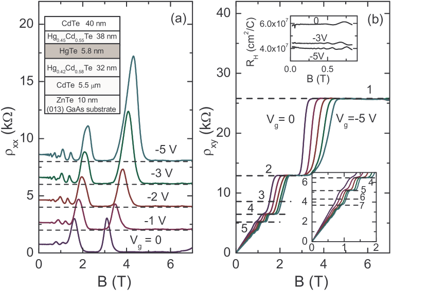
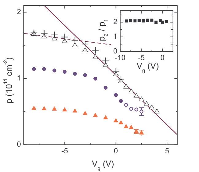
An overview of the magnetic field dependences of a longitudinal and transverse resistivity ( and , respectively) for different gate voltages () is presented in Fig. 1. Well defined quantum Hall plateaus in and minima in are evident. It should be noted that the plateaus with the numbers and [see lower inset in Fig. 1(b)] are not observed. This point will be discussed later. As clearly seen from the upper inset in Fig. 1(b), the Hall coefficient is practically independent of the magnetic field in the low-field domain T, where the Shubnikov-de Haas (SdH) oscillations are not observed yet. One can therefore assume that the density of holes can be obtained as . The gate voltage dependence of so obtained hole Hall density is presented in Fig. 2 by triangles. One can see that linearly changes with with the slope of about cm-2V-1 at V, where the hole density is less than cm-2. At V, the slope becomes much less; cm-2V-1. Note the capacitance between the gate electrode and two-dimensional channel in this structure is constant over the whole gate voltage range so that the value of cm-2 V-1 is practically the same as cm-2V-1 observed at V. Possible reasons for the decrease evident at V are considered in the end of this section. The Hall mobility , where stands for the conductivity at , increases with the increase, achieves the maximal value of about cm2/V s at cm-2, and demonstrates slight decrease with the further increase (not shown).
Another way to determine the hole density is the analysis of the SdH oscillations. The experimental SdH oscillations of are shown for several gate voltages in Fig. 3(a), while the corresponding Fourier spectra are presented in Fig. 3(b). Two maxima with frequencies and , which are shifted with the gate voltage can be easily detected in the Fourier spectra.111Note that in order to find the parameters of the energy spectrum from the SdH oscillations one should make the Fourier analysis at low enough magnetic field when the oscillations of the Fermi energy with the magnetic field can be neglected, i.e., when . Noteworthy is that the ratio of the frequencies is close to (see the inset in Fig. 2). So, the Fourier spectra are analogous to the case when the spin splitting of the Landau levels manifests itself with the magnetic field increase. In such a situation the carrier density should be determined as . If this is true in our case, we obtain which is significantly less than the hole density obtained from the Hall effect. For example, inspection of Fig. 3(b) reveals T for V that yields cm-2, whereas the Hall effect for this gate voltage gives much larger value, cm-2 (see Fig. 2).
Before discussing this discrepancy, let us point out the fact that very similar results were obtained in Ref. Ortner et al., 2002 for the HgTe quantum well of the same nominal width but with somewhat larger Hall density, cm-2 [see Fig. 3(d)]. As seen two maxima in the Fourier spectrum with the ratio of the frequencies of about two were observed also in that paper. Therewith the hole density found from the SdH oscillations turns out to be less than the Hall density.
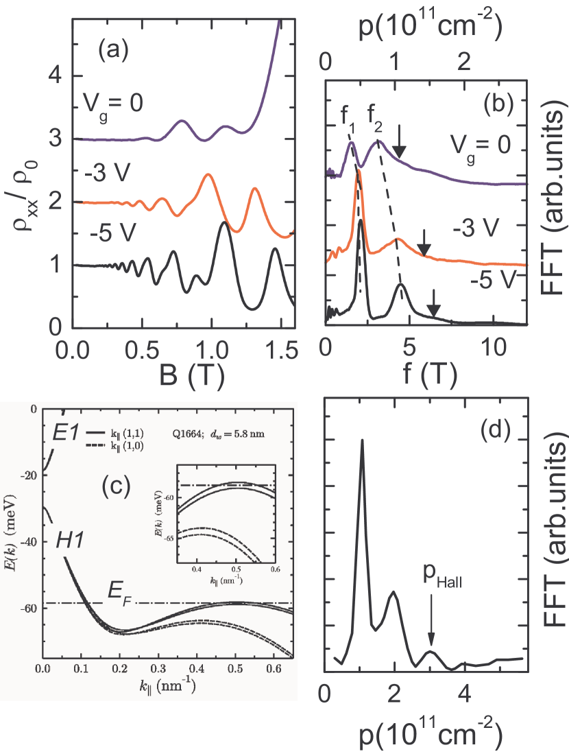
There are several possibilities to get out of this disparity, . The authors of Ref. Ortner et al., 2002 attributed this discrepancy to the peculiarity of the valence band energy spectrum. The energy spectrum calculated for the actual energy range in Ref. Ortner et al., 2002 is presented in Fig. 3(c). As seen there are additional maxima on the dispersion of the valence band in the (1,1) direction at nm-1. These maxima are situated meV lower than the top of the main maximum at . In accordance with the calculation, the authors of Ref. Ortner et al., 2002 reasoned that the experimental peak corresponding to cm-2 is two merged peaks centered at cm-2 and cm-2, which originate from the spin-orbit split and subbands at . The peak at cm-2 corresponds to the sum of the hole densities in these subbands. So, the hole density found from the SdH oscillations is about cm-2 according to the interpretation given in Ref. Ortner et al., 2002. The difference between the Hall density, cm-2 [see Fig. 3(d)] and SdH density, cm-2, which is about of cm-2, has been attributed to the holes in the four secondary maxima at nm-1. According to the authors:Ortner et al. (2002) “A peak in the Fourier spectrum due to these holes could be expected; however, this should occur at a very low frequency corresponding to cm-1 and is therefore not observed”. It is clear that in the framework of this model the decrease of the total hole density down to cm-2 should lead to the disappearance of the contribution of the carriers from the secondary maxima and, thus, should lead to agreement between the Hall and SdH densities. Unfortunately, the structure studied in Ref. Ortner et al., 2002 was ungated therefore the authors could not control the density of the carriers to check such interpretation. So, the results of Ref. Ortner et al., 2002 does not seem very conclusive.
In the structures investigated in the present paper, the difference between the density found from the SdH oscillations within proposed model and the density found from the Hall effect is observed over the whole gate voltage range, where the hole density changes from cm-2 to cm-2. Thus, the described above interpretation does not correspond to our case.
The only model that describes our results is as follows. As in Ref. Ortner et al., 2002, we suppose that the subband of spatial quantization is split by spin-orbit interaction into two subbands, and , due to asymmetry of the quantum well. But in contrast to Ref. Ortner et al., 2002, we will believe that the spin-orbit splitting is so large that the two maxima evident in our Fourier spectra originate just from these and subbands. Under this assumption the hole densities in the split subbands should be found as , where the indexes and correspond to the and , respectively. The factor two in the denominator is due to the absence of “spin” degeneracy of the split subbands. The total density in this case is the sum of and ; . The results of such a data treatment are presented in Fig. 2 within the gate voltage range from V to V, where we were able to determine reliably the frequencies for both peaks in the Fourier spectrum. One can see that the values of coincide with , to within experimental error. At V, we could determine the frequency of only low-frequency Fourier component resulting from the quantization of subband. In this case the hole densities in the second subband, , was found as and is shown in Fig. 2 by the open circles. As seen these data match the data obtained directly from the Fourier spectra at V well.
The inset in Fig. 2 shows that the ratio of the hole densities in spin-orbit split subbands is practically independent of the gate voltage and consists of about over the whole gate voltage range. So large ratio is an evidence of the giant spin-orbit splitting.222 It might be expected that the existence of two types of the carries corresponding to the two spin-orbit split subbands should reveal itself in the magnetic field dependences of Hall coefficient and longitudinal resistance. However, it is easy to check that for such a ratio between the densities and with the ratio between the mobilities of about times, the change of and in classical magnetic fields should be about % only. Really, the changes of and with magnetic field about % are observed, however it is impossible to find four parameters unambiguously from these dependencies.
At first sight the large spin-orbit splitting of the energy spectrum in the nominally almost symmetrical structure [see the inset in Fig. 1(a)] seems very surprising. However, one must take into account the peculiarity of MBE growth process of the Hg1-xCdxTe/HgTe heterostructures. There is an overpressure of Te during the growth process, therefore the Hg vacancies are presented in the structure at the end of growth. They are the acceptors in Hg1-xCdxTe, therefore major carriers in the quantum well should be the holes. Nevertheless, the heterostructures demonstrate -type conductivity after evacuation from the growth chamber as a rule. It is believed that this is because the mercury overpressure remains in the chamber after completion of growth. During the cooling, the vacancies of the mercury are annealed. When the cooling time is small, the upper barrier is converted to the -type, while the lower barrier can remain of -type. In this case, the quantum well is brought into the - junction and the strong electric field of the junction should lead to spin-orbit splitting due to the Rashba effect.Bychkov and Rashba (1984)
Thus, the analysis of the gate voltage dependences of the Hall density and SdH oscillations shows that we are dealing with the structures whose valence band is strongly split due to spin-orbit interaction. Knowing this we are in position to study the spectrum in more detail.
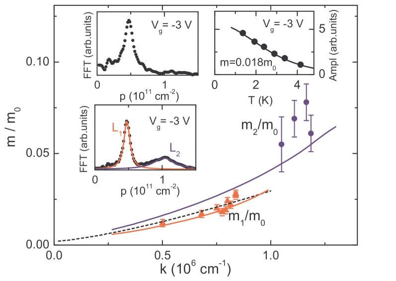
In order to do this we have determined the hole effective mass analyzing the temperature dependence of the amplitude of the SdH oscillations. As seen from the left upper inset in Fig. 4, the main contribution to the SdH oscillations at low enough magnetic field comes from the one spin-orbit split subband , which gives the lower frequency to the Fourier spectrum. Thus, the effective mass found from the SdH oscillations within this magnetic field range will correspond to the mass in the subband. As an example, the temperature dependence of the amplitude of SdH oscillations at T measured at V is shown in the right inset in Fig. 4. The fit of this dependence by the Lifshits-Kosevich formulaLifshits and Kosevich (1955) (shown by the line) gives . Such analysis performed for different gate voltages gives the quasimomentum dependence of the effective mass which is plotted in Fig. 4 by the triangles. One can see that increases significantly with increasing.
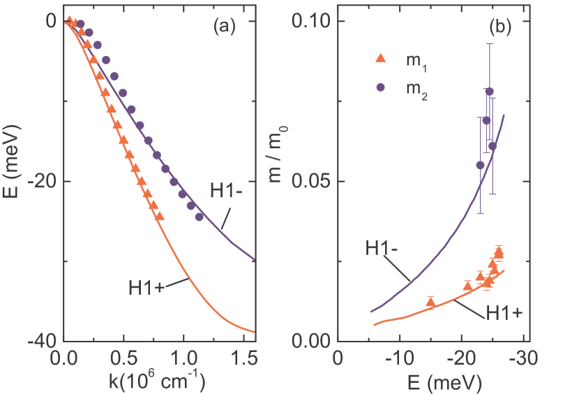
The experimental determination of the effective mass in the second subband, , is much more difficult. With this aim, we have decomposed the Fourier spectra for every temperature by fitting them by two Lorentzians, and (see the left lower inset in Fig. 4). Then, after the inverse Fourier transformation of we obtained the oscillations coming from the subband. From the temperature dependence of the amplitude of these oscillations we have found the effective mass . The results of such a data treatment are shown in Fig. 4 by the circles.
Knowing vs dependence and assuming an isotropic energy spectrum one can restore the dispersion : . Because is measured within a wider interval of , we have firstly obtained for the subband. Using the interpolation dependence shown in Fig. 4 by the dotted curve we have obtained the dependence , which is depicted in Fig. 5(a) by the triangles. To restore the dispersion of the subband we use the fact that the ratio of the hole densities in the and subbands is about over the whole gate voltage range [see the inset in Fig. 2]. So the dispersion of the subband has been obtained from the dispersion by scaling with the factor in the direction. The value of spin-orbit splitting is really gigantic: for example, it is about meV at the Fermi energy meV, i.e., approximately %, Now, when we have restored the vs dependence we can find the energy dependence of the effective masses [see Fig. 5(b)]. It is seen that increases strongly with the energy and is times larger than .
To compare the experimental results with the theory, we have calculated the energy spectrum within framework of the six-band kP model taking into account the lattice mismatch between the Hg1-xCdxTe layers forming the quantum well and CdTe buffer layer. The calculations have been performed within framework of isotropic approximation using the direct integration technique as described in Ref. Larionova and Germanenko, 1997. The run of the electrostatic potential has been obtained self-consistently from the simultaneous solution of the the Schrödinger and Poisson equations. The donor and acceptor densities in the upper and lower barriers, respectively, were supposed to be equal to cm-3. The other parameters were the same as in Refs. Zhang et al., 2001; Novik et al., 2005.
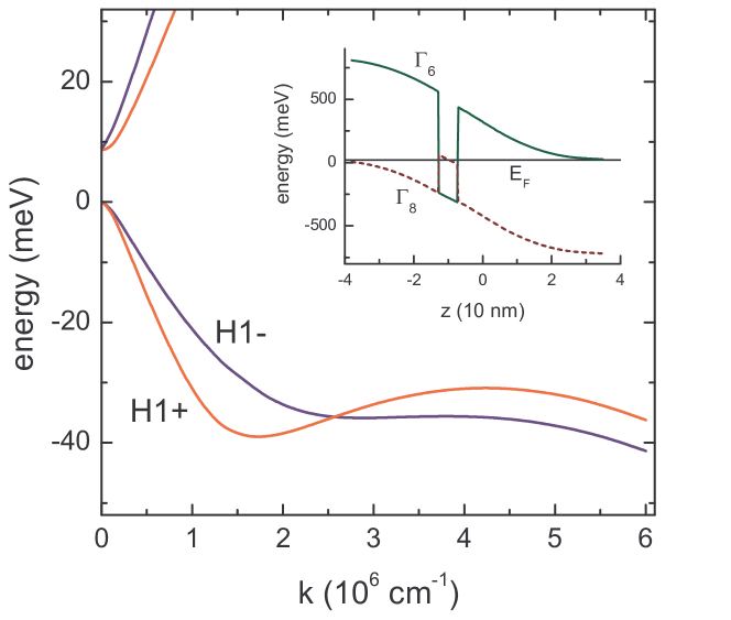
The calculated energy diagram and the dispersion law for the heterostructure H724 are shown within a wide range in Fig. 6. As clearly seen the energy spectrum of valence and conduction bands is strongly split due to the Rashba effect, therewith the positions of the branches and are interchanged at cm-1.
To compare theoretical and experimental results, we have depicted the calculated dependences , and on the same figures, where the experimental data are presented [see Fig. 4, Figs. 5(a) and 5(b), respectively]. It is evident that in the range, where the experimental data were obtained, they are in good agreement with the theoretical curves suggesting the adequacy of the model used.
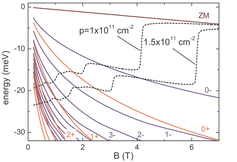
Let us now turn to the peculiarity of the quantum Hall effect mentioned in the beginning of this section and evident as the absence of the quantum Hall plateaus with the numbers and [see Fig. 1(b)]. Interestingly, the absence of the same plateaus was also observed but not commented and discussed in Ref. Ortner et al., 2002 (see Fig. 7 in that paper). To understand this feature, one should calculate the Landau levels. It can be in principle done with the use of one of technique presented in the literature.Novik et al. (2005); Zholudev et al. (2012) However, the qualitative explanation can be already obtained within much simpler semi-classical quantization approximation. The energy of the -th Landau level can be obtained in this case by substitution of instead of in the dependence , where is the magnetic length. Moreover, it must be taken into account that there is an additional zero-mode (ZM) Landau level for such a spectrum, whose position is almost independent of the magnetic field.Novik et al. (2005); Buttner et al. (2011); Zholudev et al. (2012); Minkov et al. (2013b) In Fig. 7, we have depicted the fan-chart diagram calculated in such a manner for the spectrum shown in Fig. 5(a). The dotted lines in this figure are the Fermi level calculated with the Landau levels broadening of meV for two hole densities, cm-2 and cm-2. One can see that the energy distances between the levels and , and the levels and near the Fermi level within this hole density range are noticeable less than that between the other levels. Therefore, the localized states between these Landau levels can be absent so the plateaus with the numbers and have not to be observed.
Another feature mentioned above is that the vs dependence is flattened at V when the density reaches the value cm-2 with the lowering gate voltage (Fig. 2). There are two possibilities to explain this behavior. The first one results from the peculiarity of the energy spectrum. It is easy to estimate from Fig. 5(a) that the Fermi level at cm-2 lies at the energy of about meV. As seen from Fig. 6, this value is close to the energy of secondary maxima in the dependence located at cm-1. Because of the large effective mass in these maxima the sinking speed of the Fermi level decreases strongly when these states are being occupied at V. In the presence of potential fluctuations, these states can be localized and, hence, they will not contribute to the conductivity. In this case, the Hall density will correspond to the hole density in the main maximum (while the total charge of carriers in the well will be determined by the density in all the maxima). In favour of this conclusion is the fact that the flattening of the dependence is observed in all three structures under study.
The second possibility to explain the feature under discussion is existence of localized states in the lower barrier which start to be occupied with the decreasing gate voltage leading to the same effect in the dependence just at V. We cannot exclude this mechanism at the moment.
IV Conclusion
We have studied the transport phenomena in the gated quantum well Hg1-xCdxTe/HgTe of -type conductivity with the normal energy spectrum. Analyzing the data we have reconstructed the dispersion law near the top of the valence band at cm-1. It has been shown that the hole energy spectrum is strongly split by the spin-orbit interaction, so that the ratio of the holes in the split subbands is approximately equal to two. It has been shown that the energy spectrum is strongly non-parabolic, i.e., the hole effective masses significantly increase with the energy increase. These results are well described in the framework of the kP model if one supposes that the lower barrier remains of -type, while the upper one is converted to the -type after the growth stop so that the quantum well is located in a strong electric field of - junction.
Noteworthy is that the above conclusion on the adequacy of the kP model for description of the hole energy spectrum is opposite to the conclusion made in our previous paperMinkov et al. (2013a) on the wide quantum wells with the inverted spectrum. It was there shown that the valence band spectrum is electron-like near so the top of the band is located at . The key result of the paper, however, was that the experimental and calculated hole spectra being in qualitative agreement were strongly different quantitatively within whole range of experimentally accessible quasimomentum values, cm-1.
One of the possible reasons why the theory works well in the narrow HgTe quantum wells and does not explain the data in wide wells is the following. The top of the valence band is formed from the different subbands of spatial quantization in narrow and wide quantum wells. The top is the subband in the first case and the subband in the second one. Thus it turns out that the standard kP model describing the dispersion of the subband fails to describe the spectrum of subband for whatever reason. The other reason concerns the band gap. In the quantum wells investigated in the present paper, the valence and conduction bands are separated by the gap. The systems investigated in Ref. Minkov et al., 2013a are semimetallic, therefore electrons and holes can coexist in such a case. A workability of single-particle approximation in such a situation can be really questionable and a many-particle approach could be more adequate.
Acknowledgments
We thank A. Ya. Aleshkin and M. S. Zholudev for helpful discussions. Partial financial support from the RFBR (Grant Nos. 12-02-00098 and 13-02-00322) are gratefully acknowledged.
References
References
- D’yakonov and Khaetskii (1982) M. I. D’yakonov and A. Khaetskii, Zh. Eksp. Teor. Fiz. 82, 1584 (1982), [Sov. Phys. JETP 55, 917 (1982)].
- Lin-Liu and Sham (1985) Y. R. Lin-Liu and L. J. Sham, Phys. Rev. B 32, 5561 (1985).
- Kisin and Petrosyan (1988) M. V. Kisin and V. I. Petrosyan, Fis. Tekh. Poluprovodn. 22, 829 (1988), [Sov. Phys. Semicond. 22, 523 (1988)].
- Gerchikov and Subashiev (1990) L. G. Gerchikov and A. Subashiev, Phys. Stat. Sol. (b) 160, 443 (1990).
- Bernevig et al. (2006) B. A. Bernevig, T. L. Hughes, and S.-C. Zhang, Science 314, 1757 (2006).
- Goschenhofer et al. (1998) F. Goschenhofer, J. Gerschu tz, A. Pfeuffer-Jeschke, R. Hellmig, C. R. Becker, and G. Landwehr, J. Electron. Mater. 27, 532 (1998).
- Mikhailov et al. (2006) N. N. Mikhailov, R. N. Smirnov, S. A. Dvoretsky, Y. G. Sidorov, V. A. Shvets, E. V. Spesivtsev, and S. V. Rykhlitski, Int. J. Nanotechnology 3, 120 (2006).
- König et al. (2007) M. König, S. Wiedmann, C. Brüne, A. Roth, H. Buhmann, L. W. Molenkamp, X.-L. Qi, and S.-C. Zhang, Science 318, 766 (2007).
- Brüne et al. (2010) C. Brüne, A. Roth, E. G. Novik, M. Knig, H. Buhmann, E. M. Hankiewicz, W. Hanke, J. Sinova, and L. W. Molenkamp, Nature Phys. 6, 448 (2010).
- Gusev et al. (2010) G. M. Gusev, E. B. Olshanetsky, Z. D. Kvon, N. N. Mikhailov, S. A. Dvoretsky, and J. C. Portal, Phys. Rev. Lett. 104, 166401 (2010).
- Gusev et al. (2013) G. M. Gusev, A. D. Levin, Z. D. Kvon, N. N. Mikhailov, and S. A. Dvoretsky, Phys. Rev. Lett. 110, 076805 (2013).
- Pfeuffer-Jeschke et al. (1998) A. Pfeuffer-Jeschke, F. Goschenhofer, S. J. Cheng, V. Latussek, J. Gerschütz, C. Becker, G. R. R., and G. Landwehr, Physica B 256-258, 486 (1998).
- Landwehr et al. (2000) G. Landwehr, J. Gerschütz, S. Oehling, A. Pfeuffer-Jeschke, V. Latussek, and C. R. Becker, Physica E 6, 713 (2000).
- Ortner et al. (2002) K. Ortner, X. C. Zhang, A. Pfeuffer-Jeschke, C. R. Becker, G. Landwehr, and L. W. Molenkamp, Phys. Rev. B 66, 075322 (2002).
- Kvon et al. (2011) Z. D. Kvon, E. B. Olshanetsky, E. G. Novik, D. A. Kozlov, N. N. Mikhailov, I. O. Parm, and S. A. Dvoretsky, Phys. Rev. B 83, 193304 (2011).
- Minkov et al. (2013a) G. M. Minkov, A. V. Germanenko, O. E. Rut, A. A. Sherstobitov, S. A. Dvoretski, and N. N. Mikhailov, Phys. Rev. B 88, 155306 (2013a).
- Zhang et al. (2002) X. C. Zhang, A. Pfeuffer-Jeschke, K. Ortner, C. R. Becker, and G. Landwehr, Phys. Rev. B 65, 045324 (2002).
- Zhang et al. (2004) X. C. Zhang, K. Ortner, A. Pfeuffer-Jeschke, C. R. Becker, and G. Landwehr, Phys. Rev. B 69, 115340 (2004).
- Gusev et al. (2011) G. M. Gusev, Z. D. Kvon, O. A. Shegai, N. N. Mikhailov, S. A. Dvoretsky, and J. C. Portal, Phys. Rev. B 84, 121302 (2011).
- Yakunin et al. (2012) M. V. Yakunin, A. V. Suslov, S. M. Podgornykh, S. A. Dvoretsky, and N. N. Mikhailov, Phys. Rev. B 85, 245321 (2012).
- Note (1) Note that in order to find the parameters of the energy spectrum from the SdH oscillations one should make the Fourier analysis at low enough magnetic field when the oscillations of the Fermi energy with the magnetic field can be neglected, i.e., when .
- Note (2) It might be expected that the existence of two types of the carries corresponding to the two spin-orbit split subbands should reveal itself in the magnetic field dependences of Hall coefficient and longitudinal resistance. However, it is easy to check that for such a ratio between the densities and with the ratio between the mobilities of about times, the change of and in classical magnetic fields should be about % only. Really, the changes of and with magnetic field about % are observed, however it is impossible to find four parameters unambiguously from these dependencies.
- Lifshits and Kosevich (1955) I. M. Lifshits and A. M. Kosevich, Zh. Eksp. Teor. Fiz. 29, 730 (1955), [Sov. Phys. JETP 2, 636 (1956)].
- Bychkov and Rashba (1984) Y. A. Bychkov and E. I. Rashba, J. Phys. C: Solid State Phys 17, 6039 (1984).
- Larionova and Germanenko (1997) V. A. Larionova and A. V. Germanenko, Phys. Rev. B 55, 13062 (1997).
- Zhang et al. (2001) X. C. Zhang, A. Pfeuffer-Jeschke, K. Ortner, V. Hock, H. Buhmann, C. R. Becker, and G. Landwehr, Phys. Rev. B 63, 245305 (2001).
- Novik et al. (2005) E. G. Novik, A. Pfeuffer-Jeschke, T. Jungwirth, V. Latussek, C. R. Becker, G. Landwehr, H. Buhmann, and L. W. Molenkamp, Phys. Rev. B 72, 035321 (2005).
- Zholudev et al. (2012) M. S. Zholudev, A. V. Ikonnikov, F. Teppe, M. Orlita, K. V. Maremyanin, K. E. Spirin, V. I. Gavrilenko, W. Knap, S. A. Dvoretskiy, and N. N. Mihailov, Nanoscale Research Letters 7, 534 (2012).
- Buttner et al. (2011) B. Buttner, C. X. Liu, G. Tkachov, E. G. Novik, C. Brune, H. Buhmann, E. M. Hankiewicz, P. Recher, B. Trauzettel, S. C. Zhang, and L. W. Molenkamp, Nature Phys. 7, 418 (2011).
- Minkov et al. (2013b) G. M. Minkov, A. V. Germanenko, O. E. Rut, A. A. Sherstobitov, S. A. Dvoretski, and N. N. Mikhailov, Phys. Rev. B 88, 155306 (2013b).