Gate-tunable coherent perfect absorption of terahertz radiation in graphene
Abstract
Perfect absorption of radiation in a graphene sheet may play a pivotal role in the realization of technologically relevant optoelectronic devices. In particular, perfect absorption of radiation in the terahertz (THz) spectral range would tremendously boost the utility of graphene in this difficult range of photon energies, which still lacks cheap and robust devices operating at room temperature. In this work we show that unpatterned graphene flakes deposited on appropriate substrates can display gate-tunable coherent perfect absorption (CPA) in the THz spectral range. We present theoretical estimates for the CPA operating frequency as a function of doping, which take into account the presence of common sources of disorder in graphene samples.
pacs:
78.67.Wj, 42.25.Bs, 73.20.MfIntroduction.—Graphene geim_naturemater_2007 ; antonio_rmp_2009 ; condrmp ; Katsnelsonbook has been shown to possess a variety of remarkable optical, electronic, and mechanical properties, the scientific and technological implications of which are still being explored novoselov_nature_2012 ; ferrari_roadmap_2014 . It has had a notable impact on the fields of photonics and optoelectronics bonaccorso_naturephoton_2010 ; koppens_nanolett_2011 ; grigorenko_naturephoton_2012 , where researchers have identified applications in devices such as photodetectors, saturable absorbers, and ultrafast lasers. In the photonics context, graphene is a two-dimensional (2D) conductor that supports plasmons with unusually tunable properties koppens_nanolett_2011 ; grigorenko_naturephoton_2012 .
This paper explores the theoretical limitations to total optical absorption for an unpatterned graphene sheet lying on a substrate, with light incident from free space onto the graphene. This represents a common experimental situation where graphene is deposited onto a prepared surface geim_naturemater_2007 . A single sheet of undoped graphene has a single-pass absorptivity of , where is the quantum electrodynamics fine-structure constant finesci . This low absorptivity, which points to important applications for graphene as a transparent conductive film bonaccorso_naturephoton_2010 , can be derived from the frequency-independent sheet conductivity of under conditions of negligible impurity and substrate scattering. On the other hand, we shall show that it is possible to achieve coherent perfect absorption (CPA) at a specific frequency in an unpatterned graphene sheet, provided the graphene is doped to a specific level. CPA is a manifestation of critical coupling, a phenomenon that is commonly exploited in integrated photonics cai ; yariv . In critically-coupled systems, the multiple coherent paths taken by incident photons to exit an absorbing system—by scattering or reflection—interfere destructively, resulting in 100% conversion into the absorption channel. (The CPA phenomenon can be studied in a general optical scattering context cpa ; wan11 , but here we consider a single input and output channel. Single-channel critical coupling, utilizing a thin absorbing layer of organic aggregate, has previously been demonstrated experimentally bulovic .) In the context of unpatterned graphene, CPA requires a specific universal value of , the real part of the optical sheet conductivity. Using random phase approximation (RPA)-Boltzmann transport theory condrmp ; Adam07 ; Jang ; Adam08 , we demonstrate the existence of a threshold (minimum) doping level, which is typically around , depending on the impurity density. Furthermore, we derive the frequency at which the CPA condition is met at each doping level. The operating frequency for CPA lies in the THz range, up to for realistic doping levels and substrates. The only additional requirements for CPA to occur are that the substrate should be perfectly reflective and that the phase of its reflection coefficient should have a specific value; in particular, the optical quality factor does not enter into the result. By electrically doping the graphene, it should be possible to dynamically modulate between nearly zero absorption and 100% absorption. CPA in the THz spectral range may offer an alternative route to the fabrication of graphene-based THz modulators and detectors NEST , which currently operate, for the most part, on the basis of the Dyakonov-Shur principle DS principle .
Previous works have suggested enhancing optical absorption in graphene through several different approaches. One is to embed graphene in an optical cavity: at the frequency of a cavity resonance, the total absorption, due to multiple passes of recycled photons, can be much larger than the single-pass absorption, in principle reaching 100%. Perfect absorption has recently been demonstrated experimentally with a Fabry-Pérot microcavity engel_naturecommun_2012 ; furchi_nanolett_2012 , and enhanced absorption of has been demonstrated in an attenuated total reflectance configuration pirruccio_acsnano_2013 . For applications in the far-infrared and THz, other promising routes towards enhanced or even perfect absorption involve patterning the graphene to exploit local plasmon resonances fei_nature_2012 ; chen_nature_2012 ; grigorenko_naturephoton_2012 ; koppens_nanolett_2011 ; thongrattanasiri_prl_2012 ; nikitin_prb_2012 ; Muhammad_OE , or patterning the substrate to exploit metamaterial resonances aires_prb . Thongrattanasiri et al. thongrattanasiri_prl_2012 , for example, have argued that light absorption can occur in periodic arrays of doped graphene nanodisks on a reflective substrate. Similar results were obtained by Nikitin et al. nikitin_prb_2012 for arrays of graphene ribbons.
In contrast to the above-mentioned configurations, we consider here a single graphene sheet on a reflective substrate. The graphene is not embedded in an optical cavity, which limits photon recycling. Furthermore, unlike Refs. thongrattanasiri_prl_2012, ; nikitin_prb_2012, ; Muhammad_OE, , the graphene sheet is unpatterned, and lacks the transverse confinement giving rise to local plasmon resonances. Apell et al. have theoretically studied the absorption in a similar configuration, and shown that the absorption can be enhanced by tuning the chemical potential of the graphene sheet as well as the dielectric environment; however, the origins of this enhancement, and the exact configuration required to achieve 100% absorption, were not clearly identified apell . Liu et al. have similarly argued that absorption can be enhanced, and suggested using a substrate containing a metal back reflector Liu1 ; Liu2 . However, we shall see that the absorption can in principle reach 100%, and derive the exact conditions for this to occur. These results might be generalizable to other materials with conducting surface states, such as topological insulators adam12 .
Theory of CPA in a doped graphene sheet.—Consider a 2D conducting sheet suspended in air, parallel to the - plane. For normally-incident electromagnetic plane waves propagating in the direction the transfer matrix across the sheet is
| (1) |
where is the identity matrix and with the optical sheet conductivity and
| (2) |
Note that . Eq. (1) implies the well-known fact that such a sheet can absorb at most of light incident from one side. This limit can be overcome by placing an optical cavity (or “substrate”) on the opposite side of the sheet. Let us assume that the substrate is perfectly reflecting, with a complex reflection coefficient . Then the reflection coefficient for the entire system (sheet plus substrate) satisfies
| (3) |
where is the wave intensity on the mirror side of the graphene sheet. Hence, from Eq. (1),
| (4) |
The absorbance is then given by . Note that material losses in the substrate can be modeled by setting ; however, we will assume no such losses.
From Eq. (4), we see that CPA, i.e. , occurs when the conductivity satisfies
| (5) |
Note that as long as reaches the value , then regardless of the value of there is always some value of that satisfies the second part of (5). This also implies that CPA cannot occur in an ideal undoped graphene sheet since, as we noticed earlier after Eq. (2), . Conditions similar to (5) were also derived in Eqs. (11)-(12) of Ref. apell, .
In a doped graphene sheet, the optical conductivity can be much larger than at frequencies , where is the Fermi energy. In this frequency regime, the conductivity has negligible contribution from inter-band transitions and is well described by the Drude formula Ashcroft_and_Mermin ; footnote_tau ; nomura_prl_2006 ; primer :
| (6) |
where is the dc conductivity and is the dc transport scattering time. At THz frequencies, it is important to note that varies with the doping level Adam07 ; Jang ; Adam08 ; condrmp , and we shall take this into account in the following analysis (in Ref. Liu2, , was approximated as doping-independent). Comparing to Eq. (5), we find that CPA occurs at the frequency
| (7) |
For this to be satisfied, we require
| (8) |
The dc transport scattering time depends on the doping level in a way that is controlled by the various electron-impurity and electron-phonon scattering mechanisms. In this work we concentrate on the former, which dominates at sufficiently low temperatures, and, more precisely, we consider scattering of electrons against charged and short-range impurities. We denote by the symbol () the contribution to that stems from charged impurity (short-range disorder) scattering:
| (9) |
In the regime of doping we are interested in, both contributions can be safely determined from Boltzmann transport theory (in conjunction with the RPA to treat screening) Adam07 ; Jang ; Adam08 ; condrmp . For simplicity, we assume that the charged impurities are located on the graphene sheet: this assumption reduces the number of parameters of the theory, allows a complete analytical treatment of charged-impurity scattering, and can be easily relaxed by allowing a finite average distance between the impurities and graphene. In the case the result is
| (10) | ||||
| (11) |
where
| (12) |
with . Here, is the carrier density, related to the Fermi frequency by where is the density-independent Fermi velocity () and is the Fermi wave number; is the density of charged impurities; and , with the average dielectric constant of the materials surrounding the graphene flake, is the so-called “graphene fine structure constant” kotov_rmp_2012 , i.e. the ratio of the electron-electron interaction energy scale () to the kinetic energy scale (). In Eq. (11), is the limiting conductivity when the scattering is purely short-range. The value of can be determined condrmp by fitting the sub-linear dependence of the conductivity on density in the high-density regime.
Applying Eqs. (9)-(12) to Eq. (8), we find that CPA requires
| (13) |
The first inequality in (13) sets the limits for the number of defects in graphene (such as vacancies or chemisorbed dopants) and is easily satisfied in most experiments on exfoliated and CVD grown graphene without the intentional addition of defects, where . The second inequality describes the minimum carrier doping that must be present (relative to the charged impurity density). For a relatively large impurity concentration of , this corresponds to a minimum doping of . Doping levels of this order are routinely obtained in experiments condrmp ; Jang ; sometransportexperiments ; however, in the present design it may be challenging to achieve this purely via back-gating, due to the thickness of the dielectric substrate required for THz operating frequencies. This difficulty is discussed in the next section.
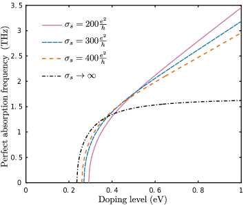
Numerical results and discussion.—Fig. 1 shows the operating frequency for CPA, , as a function of , as calculated from Eq. (7) with Eqs. (9)-(12). We observe a rapid increase in with above the threshold doping level, which, as noted above, depends on and . When short-range scattering is negligible (), saturates for large dopings at the value
| (14) |
For and , this corresponds to a maximum frequency of . When is non-negligible, does not saturate with increasing , but instead increases linearly at high doping levels. These operating frequencies correspond to energies in the range (), much lower than the doping level, which is . Hence, the Drude conductivity model in Eq. (6) is valid throughout.
When the system is tuned for perfect absorption at , light incident at nearby frequencies is also strongly absorbed. The absorption frequency bandwidth is determined by as well as the frequency dispersion of the substrate reflection phase in Eq. (5). The -limited frequency bandwidth is extremely large. In Eq. (4), assuming that is frequency-independent, if perfect absorption occurs at frequency , then at frequency ,
| (15) |
Eq. (6) then gives, for the absorbance,
| (16) |
Hence, the absorption bandwidth would simply be the inverse of the transport scattering time. For the parameters we have considered, 10 THz, on the order of itself. For practical purposes, therefore, the absorption bandwidth is limited by the detuning of . The substrate could be engineered to minimize this detuning; for example, one could use low-order modes for which has bandwidth on the order of the operating frequency.
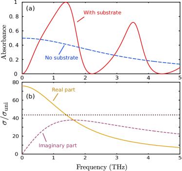
Fig. 2 shows the absorbance for a graphene sheet on a SiO2 substrate with a metal reflector on the far end, which is tuned to produce perfect absorption at . The system operates at the lowest-order cavity mode, with the cavity length being approximately equal to a quarter-wavelength. A broad absorption resonance, of relative bandwidth , is indeed observed. The bandwidth could be further optimized by designing a non-uniform cavity. By comparison, the relative absorption bandwidth was in the experiments demonstrating the principle of CPA in optical cavities cpa ; wan11 .
In the calculations of Fig. 2, we gave the substrate a thickness of m, chosen to achieve the phase shift satisfying the CPA condition (5). This thickness is determined by the choice of an operating frequency in the THz range, and is substantially larger than in typical electric gating experiments condrmp ; Jang ; sometransportexperiments , where nm substrates are used. With our thick dielectric substrate, achieving the necessary doping level of around may be challenging—though not impossible, since the breakdown voltage scales linearly and the capacitance inversely with distance. More realistically, one could first dope the graphene with charged impuritiesChen2008 , polymer electrolytes Efetov2010 , or organic molecules like F4TCNQ Coleti2010 ; Kim2012 , in order to increase the carrier density while remaining transparent to THz radiation. In these cases, the back-gate could still be used to fine-tune the carrier density to meet the CPA criteria.
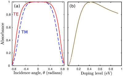
The absorption is robust against variations in the incidence angle. For oblique incidence, two different polarizations should be considered: transverse magnetic (TM; magnetic field parallel to the plane of the graphene sheet) and transverse electric (TE; electric field parallel to the plane). For incidence angle , the transfer matrix across the graphene sheet is
| (17) |
The reflection coefficients are thus obtained by replacing with in Eq. (4). The cavity phase delay also depends on . Supposing we have optimized the structure for perfect absorption at normal incidence footnote_optimization_at_finite_theta (), the reflectance can be calculated as a function of for each polarization; the result is
| (18) |
This is demonstrated numerically in Fig. 3(a).
The system can also be detuned from the CPA condition by varying the doping level, e.g. via the electrochemical potential of the metallic gate acting as the back-reflector thongrattanasiri_prl_2012 . As shown in Fig. 3(b), one can tune between perfect absorption at the tailored doping level and close to zero absorption at low doping levels.
As a final note, we would like to point out that even if the conductivity is nowhere near the magic value , the total absorption can generally be reduced to zero. This suppression of absorption is an interference effect. The absorptivity of the graphene sheet remains constant, but the total absorption goes to zero since the local intensity at the graphene sheet vanishes (i.e. the sheet lies at a node of a standing wave). This effect is similar to those reported in Ref. node, , where the absorption goes to zero (a large value) when there is a node (anti-node) at the position of the thin absorbing layer.
Acknowledgements.—CYD acknowledges support from the National Research Foundation Singapore under its Fellowship program (NRF-NRFF2012-01). SA is supported by the National Research Foundation Singapore under its Fellowship program (NRF-NRFF2012-01). MP acknowledges support by the EC under Graphene Flagship (contract no. CNECT-ICT-604391) and the Italian Ministry of Education, University, and Research (MIUR) through the program “FIRB–Futuro in Ricerca 2010”–Project PLASMOGRAPH (Grant No. RBFR10M5BT).
References
- (1) A. K. Geim and K. S. Novoselov, Nature Mater. 6, 183 (2007).
- (2) A. H. Castro Neto, F. Guinea, N. M. R. Peres, K. S. Novoselov, and A. K. Geim, Rev. Mod. Phys. 81, 109, (2009).
- (3) S. Das Sarma, S. Adam, E. H. Hwang, and E. Rossi, Rev. Mod. Phys. 83, 407 (2011).
- (4) M. I. Katsnelson, Graphene: Carbon in Two Dimensions (Cambridge University Press, Cambridge, 2012).
- (5) K. S. Novoselov, V. I. Fal’ko, L. Colombo, P. R. Gellert, M. G. Schwab, and K. Kim, Nature 490, 192 (2012).
- (6) A. C. Ferrari et al., Nanoscale (2014).
- (7) F. Bonaccorso, Z. Sun, T. Hasan, and A. C. Ferrari, Nature Photon. 4, 611 (2010).
- (8) F. H. L. Koppens, D. E. Chang, and F.J. García de Abajo, Nano Lett. 11, 3370 (2011).
- (9) A. N. Grigorenko, M. Polini, and K. S. Novoselov, Nature Photon. 6, 749 (2012).
- (10) A. B. Kuzmenko, E. van Heumen, F. Carbone, and D. van der Marel, Phys. Rev. Lett. 100, 117401 (2008); R. R. Nair, P. Blake, A. N. Grigorenko, K. S. Novoselov, T. J. Booth, T. Stauber, N. M. R. Peres, and A.K. Geim, Science 320, 1308 (2008); F. Wang, Y. Zhang, C. Tian, C. Girit, A. Zettl, M. Crommie, and Y. R. Shen, Science 320, 206 (2008); K. F. Mak, M. Y. Sfeir, Y. Wu, C. H. Lui, J. A. Misewich, and T. F. Heinz, Phys. Rev. Lett. 101, 196405 (2008).
- (11) M. Cai, O. Painter, and K. J. Vahala, Phys. Rev. Lett. 85, 74 (2000).
- (12) A. Yariv, IEEE Phot. Tech. Lett. 14, 483 (2002).
- (13) Y. D. Chong, L. Ge, H. Cao, and A. D. Stone, Phys. Rev. Lett. 105, 053901 (2010).
- (14) W. Wan, Y. D. Chong, L. Ge, H. Noh, A. D. Stone, and H. Cao, Science 331, 889 (2011).
- (15) J. Tischler, M. S. Bradley, and V. Bulović, Opt. Lett. 31, 2045 (2006).
- (16) S. Adam, E. H. Hwang, V.M. Galitski, and S. Das Sarma, Proc. Natl. Acad. Sci. (U.S.A.) 104, 18392 (2007).
- (17) C. Jang, S. Adam, J. H. Chen, E.D. Williams, S. Das Sarma, and M. S. Fuhrer, Phys. Rev. Lett. 101 146805 (2008).
- (18) S. Adam, E. H. Hwang, and S. Das Sarma, Physica E 40, 1022 (2008).
- (19) See e.g. L. Vicarelli, M. S. Vitiello, D. Coquillat, A. Lombardo, A. C. Ferrari, W. Knap, M. Polini, V. Pellegrini, and A. Tredicucci, Nature Mat. 11, 865 (2012); D. Spirito, D. Coquillat, S. L. De Bonis, A. Lombardo, M. Bruna, A. C. Ferrari, V. Pellegrini, A. Tredicucci, W. Knap, and M. S. Vitiello, Appl. Phys. Lett. 104, 061111 (2014).
- (20) A. Tomadin and M. Polini, Phys. Rev. B 88, 205426 (2013).
- (21) M. Engel, M. Steiner, A. Lombardo, A. C. Ferrari, H. v. Loehneysen, P. Avouris, and R. Krupke, Nature Commun. 3, 906 (2012).
- (22) M. Furchi, A. Urich, A. Pospischil, G. Lilley, K. Unterrainer, H. Detz, P. Klang, A. M. Andrews, W. Schrenk, G. Strasser, and T. Mueller, Nano Lett. 12, 2773 (2012).
- (23) G. Pirruccio, L. M. Moreno, G. Lozano, and J. G. Rivas, ACS Nano 7, 4810 (2013).
- (24) Z. Fei, A.S. Rodin, G.O. Andreev, W. Bao, A.S. McLeod, M. Wagner, L. M. Zhang, Z. Zhao, M. Thiemens, G. Dominguez, M. M. Fogler, A. H. Castro Neto, C. N. Lau, F. Keilmann, and D. N. Basov, Nature 487, 82 (2012).
- (25) J. Chen, M. Badioli, P. Alonso-González, S. Thongrattanasiri, F. Huth, J. Osmond, M. Spasenović, A. Centeno, A. Pesquera, P. Godignon, A. Zurutuza Elorza, N. Camara, F. J. García de Abajo, R. Hillenbrand, and F. H. L. Koppens, Nature 487, 77 (2012).
- (26) S. Thongrattanasiri, F. H. L. Koppens, and F. Javier García de Abajo, Phys. Rev. Lett. 108, 047401 (2012).
- (27) A. Yu. Nikitin, F. Guinea, F. J. Garcia Vidal, and L. Martin Moreno, Phys. Rev. B85, 081405(R) (2012).
- (28) M. Amin, M. Farhat, and H. Bağcı, Opt. Express 21 , 29938 (2013).
- (29) A. Ferreira and N. M. R. Peres Phys. Rev. B86, 205401 (2012)
- (30) S. P. Apell, G. W. Hanson, and C. Hägglund, arXiv 1201.3071
- (31) J.-T. Liu, N.-H. Liu, J. Li, X.J. Li, and J.-H. Huang, Appl. Phys. Lett. 101, 052104 (2012).
- (32) J.-T. Liu, N.-H. Liu, L. Wang, X.H. Deng, and F.-H. Su, arxiv:1311.2120
- (33) S. Adam, E.H. Hwang, and S. Das Sarma Phys. Rev. B85, 235413 (2012).
- (34) N. W. Ashcroft and N. D. Mermin, Solid State Physics (Saunders College, New York, 1976).
- (35) In principle, should vary with frequency, with its limit corresponding to the dc transport scattering time. However, since we will be working at frequencies , the frequency dependence of is negligible and will be neglected.
- (36) K. Nomura and A. H. MacDonald, Phys. Rev. Lett. 96, 256602 (2006).
- (37) Y. V. Bludov, A. Ferreira, N. M. R. Peres, and M. Vasilevskiy, Int. J. Mod. Phys. B 27, 1341001 (2013).
- (38) V. N. Kotov, B. Uchoa, V. M. Pereira, F. Guinea, and A. H. Castro Neto, Rev. Mod. Phys. 84, 1067 (2012).
- (39) See e.g. K. S. Novoselov, A. K. Geim, S. V. Morozov, D. Jiang, Y. Zhang, M. I. Katsnelson, I. V. Grigorieva, S. V. Dubonos, and A. A. Firsov, Nature 438, 197 (2005); Y. Zhang, Y. W. Tan, H. L. Stormer, and P. Kim, Nature 438, 201 (2005); X. Hong, K. Zou, and J. Zhu, Phys. Rev. B80, 241415(R) (2009); J. Yan and M. S. Fuhrer, Phys. Rev. Lett. 107, 206601 (2011).
- (40) J.-H. Chen, C. Jang, S. Adam, M. S. Fuhrer, E. D. Williams, and M. Ishigami, Nat. Phys. 4, 377 (2008).
- (41) D. K. Efetov and P. Kim, Phys. Rev. Lett. 105, 256805 (2010).
- (42) C. Coletti, C. Riedl, D. S. Lee, B. Krauss, L. Patthey, K. von Klitzing, J. H. Smet, and U. Starke, Phys. Rev. B 81, 235401 (2010).
- (43) D. Kim et al., Nat. Phys. 8, 459 (2012).
- (44) Note that one can achieve CPA at an incident angle . In this case, CPA can only occur for one polarization at a time. The CPA conditions at finite are and , for TM and TE polarizations, respectively. Therefore, for a TM (TE) mode we need larger (smaller) than .
- (45) J. Zhang, K.F. MacDonald, and N.I. Zheludev, Light: Sci. and Appl. e18, 1 (2012).