Electromotive Force Generated by Spin Accumulation in FM/-GaAs Heterostructures
Abstract
We report on a method of quantifying spin accumulation in Co2MnSi/-GaAs and Fe/-GaAs heterostructures using a non-magnetic probe. In the presence of a large non-equilibrium spin polarization, the combination of a non-constant density of states and energy-dependent conductivity generates an electromotive force (EMF). We demonstrate that this signal dephases in the presence of applied and hyperfine fields, scales quadratically with the polarization, and is comparable in magnitude to the spin-splitting. Since this spin-generated EMF depends only on experimentally accessible parameters of the bulk material, its magnitude may be used to quantify the injected spin polarization in absolute terms.
pacs:
72.25.Dc, 72.25.Hg, 85.75.-dDespite recent progress in demonstrating electrical spin injection and detection in a wide variety of semiconducting materials systemsLou et al. (2007); Ciorga et al. (2009); Salis et al. (2011); Uemura et al. (2011); van ’t Erve et al. (2007); Appelbaum et al. (2007); Dash et al. (2009); Suzuki et al. (2011); Jansen et al. (2012); Tombros et al. (2007); Zhou et al. (2011); Saito et al. (2013); Manzke et al. (2013); Akiho et al. (2013); Han et al. (2013), quantitative comparison among these experimental efforts is hindered primarily by difficulties in distinguishing between bulk and interfacial effects. All-electrical spintronic devices typically utilize ferromagnetic (FM) elements for both the generation and detection of spin accumulation in a non-magnetic channel. The resulting spin-dependent signal is thus a convolution of several processes: spin-injection (interface), spin-transport (bulk), and spin-detection (interface). Isolating the channel or either interface for characterization requires assumptions about the behavior of the other elements, which are not independently measurable. One possible resolution is to detect the spin accumulation via non-magnetic means, such as the inverse spin-Hall effectValenzuela and Tinkham (2006); Olejník et al. (2012). However, to serve as the basis for comparison across several materials systems, the parameters for any such spin-to-charge conversion must also be well-known functions of temperature and composition.
In this letter, we report on a different method of detecting the injected spin polarization in Co2MnSi/-GaAs and Fe/-GaAs heterostructures. In complete analogy with thermoelectric effects, the local increase in free energy density required to establish a non-equilibrium spin accumulation profile also generates an accompanying electromotive force (EMF). This is the inverse of the ability of drift currents to elongate or contract the effective spin diffusion lengthYu and Flatté (2002). Under open circuit conditions, this EMF may be detected as an electrostatic potential shift by ferromagnetic and non-magnetic contacts alike. The possibility of observing such an effect was first demonstrated by Vera-Marun et al. Vera-Marun et al. (2011, 2012) in graphene nanostructures. We show that for degenerately doped -GaAs, this effect is greatly enhanced in the regime of large spin polarization and may exceed the magnitude of the signals observed by traditional ferromagnetic detection techniques. One key advantage of this spin-to-charge conversion is that it may be characterized by independently accessible parameters of the channel material, allowing the polarization to be determined in absolute terms.
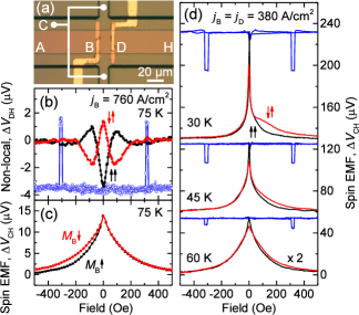
Epitaxial (001) Co2MnSi/-GaAs and Fe/-GaAs heterostructures were grown by molecular beam epitaxy and consist of a thick Si-doped channel , highly doped Schottky barrier, (, ), and ferromagnetic layerLou et al. (2007). Standard lithographic and etching techniques were used to subtractively process lateral spin-valve devices with the pattern shown in Fig. 1(a). Two ferromagnetic contacts, labeled B and D, were positioned on either side of a central Hall cross for the purposes of electrical spin injection and ferromagnetic detection. Fig. 1(b) shows typical non-local spin valve and Hanle effect curves observed at contact D for both the parallel and antiparallel configurations with a forward current bias of applied to contact B. Low-order polynomials were subtracted from all curves displayed in Fig. 1 using points outside the regions of interest to eliminate ordinary magnetoresistive contributions. At , the center-to-center separation between the contacts corresponds to approximately four spin diffusion lengths as determined from standard charge and spin transport measurements on companion devicesLou et al. (2007). The current and voltage counter-electrodes, labeled A and H respectively, are located away (not shown). These data establish the presence of a net spin current flowing into the channel and that contact D functions properly as a polarized detector of only one component of the non-equilibrium spin accumulation.
This spin accumulation was also detected as a common voltage shift in the central Hall arms, labeled C. These arms, each of length , were shorted together into a single contact to eliminate any contributions from charge- or inverse spin-Hall effects. Fig. 1(c) shows a large spin-dependent signal at contact C obtained under identical conditions as the Hanle curves in Fig. 1(b). In contrast to the signal observed at ferromagnetic detector D, the spin-dependent signal at contact C does not reverse sign upon reversal of the magnetization state of the injector (contact B). A Hanle effect of the same sign (not shown) was also observed when contact D was used as the injector for both magnetization states. These observations indicate that unlike the case of detection with a ferromagnet, which is only sensitive to a particular component of the polarization, the potential shift at contact C is sensitive to the total magnitude of the spin accumulation in the channel. This is supported by the observation that the width of the resulting line-shape in Fig. 1(c) matches the envelope of the Hanle curve shown in Fig. 1(a).
To further demonstrate that the observed potential shift depends on the total magnitude of the spin accumulation in the channel (although not its overall sign), two separate forward current biases were applied simultaneously to contacts B and D with contact A serving as the counter-electrode for both current sources. With both ferromagnetic contacts functioning as spin injectors, the total magnitude of the spin accumulation in the channel was increased (decreased) by aligning the magnetization of the two contacts parallel (anti-parallel) to each otherVera-Marun et al. (2012). As shown in Fig. 1(d), this allows observation of a spin valve effect at non-magnetic probe C when a magnetic field is swept along the in-plane ferromagnetic easy axis [110]. The switching events occurring at are the same as those observed in Fig. 1(b).
Fig. 1(d) shows the corresponding Hanle curves obtained by sweeping the magnetic field normal to the plane of the device. The difference between the parallel and anti-parallel Hanle curves at equals that of the spin valve signal, demonstrating that the signal at contact C is sensitive to the superposition of the spin accumulation arising from both ferromagnetic injectors B and D. The Hanle line-shape broadens at higher temperatures as expected due to an increased spin relaxation rate, with both Hanle curves trending to zero at higher applied field.
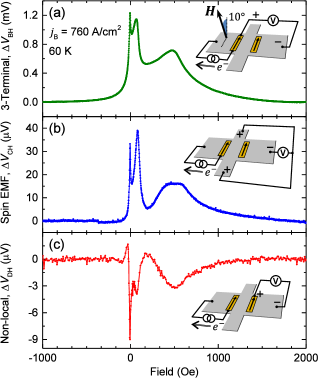
The additional low-field features in Fig. 1(d) at low temperatures are caused by hyperfine interactions with dynamically polarized nuclei, which exert large effective Overhauser fields on the electron spin dynamicsPaget (1981); Kölbl et al. (2012). This necessitates a more complex interpretation of Hanle line-shapesChan et al. (2009), yet also makes possible a robust test of whether a particular signal originates from spin-dependent processes. In the oblique Hanle geometry shown in Fig. 2, the magnetic field is applied at an intermediate angle between the device normal and the ferromagnetic easy axis. In this configuration, two additional satellite peaks appear at field values where the Overhauser field partially or wholly cancels the applied field. This cancellation reduces the Hanle dephasing effect and allows the electron spin ensemble to re-polarize. Fig. 2(a), (b) and (c) show the voltage measured on a second Co2MnSi device at contacts B (three-terminal), C (spin-generated EMF), and D (non-local) respectively as the field is swept at a constant ° orientation from the device normal. The appearance of satellite peaks at comparable positions in all three measurements provides conclusive evidence that the voltage shift observed at contact C is a direct measure of the spin accumulation in the channel. Since the sign of the Overhauser field in bulk GaAs is knownPaget et al. (1977), the position of the satellite peaks at positive field indicates majority spin accumulation in the channel. Note that the sign of the Hanle curve in Fig. 2(a) is opposite that of Fig.2(c) due to the inverted sign of the ferromagnetic detection efficiency at high forward biasCrooker et al. (2009).
The current density for spin-up (spin-down) electrons is given by the gradient of the total electrochemical potential as . denotes the number density-dependent chemical potentials and is the electrostatic potential common to both spin-bands. Following the approach in Ref. Yu and Flatté (2002), we make the assumption that the conductivity of each band is proportional to the number density with a spin-independent mobility . This allows the net charge current density to be written as
| (1) |
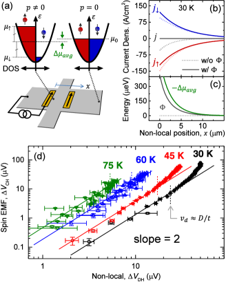
where is the fractional number polarization, is the total carrier concentration, and is the channel conductivity. Due to the presence of the first two terms, a ‘pure’ non-local spin current () cannot be achieved without establishing a non-zero electrostatic potential gradient . In the presence of a spin accumulation, the first term of Eq. 1 is non-zero due to the asymmetric shift of and relative to the unpolarized state. This is shown schematically in Fig. 3(a), where the decrease in is due to the non-constant density of states. The second term in Eq. 1 originates from the energy dependence of the conductivity, which for the Drude form above may be expressed in terms of the population imbalance of the two spin sub-bands. The dashed lines in Fig. 3(b) show the asymmetric nature of and for a typical polarization profile at 30 K (, ) in the absence of an electrostatic potential gradient . Here denotes the (non-local) position to the right of the injector contact. The solid lines indicate the steady-state condition after taking into account the spin-generated EMF.
For small polarizations , we can Taylor expand and about the background concentration :
| (2) |
where . This allows Eq. 1 to be simplified as
| (3) |
with
| (4) |
where the diffusion constant is defined via the Einstein relation Ashcroft and Mermin (1976). The first term in Eq. 4 is analogous to the first order term in the Sommerfeld expansion used to analyze the Seebeck effectAshcroft and Mermin (1976); Johnson and Lark-Horovitz (1953). The second term, absent in the usual Seebeck analysis, appears as a consequence of the imbalance in the number of carriers in the two spin sub-bands and is formally equivalent to the contribution discussed in Ref. Vera-Marun et al. (2011). For a parabolic density of states with effective mass , the function may be obtained by numerically inverting the usual relation , where is the quantum concentration and is the Fermi-Dirac integralSmith (1978). The pre-factor takes on a value of in the degenerate case and vanishes in the non-degenerate limit . Typical values for and are shown in Fig. 3(c) for a concentration of (Fermi energy, ) at .
In the non-local region where , Eq. 3 gives the electrostatic potential as . This may be regarded as a source of EMF which scales quadratically with the spin accumulation. This is in contrast to the non-local spin valve signal which scales linearly: , where is the FM spin detection efficiency. Fig. 3(d) shows the Hanle and spin valve magnitudes observed at contacts C and D plotted against each other on a log-log plot while varying the current bias applied to injector contact B. The data at low bias confirm the predicted slope of two. The departure from quadratic behavior at high bias is caused by drift currents which redistribute more of the polarization toward the interfacial region which, as discussed below, sets the boundary condition for observing the spin-generated EMF at contact C. The onset of this drift effect occurs when the effective spin diffusion lengthYu and Flatté (2002) becomes smaller than the channel thickness , i.e. drift velocity as indicated by the vertical dashed lines in Fig. 3(d).
To extract an absolute polarization from the magnitude of the voltage shift observed at contact C, we note that the electric field within the metallic interfacial regions is zero . Here is a unit vector normal to the surfaces of the contact regions B and D. The importance of the this condition is two-fold. First, it allows the shift in to be non-zero even in regions where . The layers beneath contacts B and D effectively short out any transverse potential dropIsenberg et al. (1948) across the width of the channel, allowing observation of a signal at contact C. Second, because the shorting effect causes the shift in to differ from , Eq. 3 implies the existence of divergenceless eddy currents sustained by the non-equilibrium spin polarization. These eddy currents circulate through the region into the bulk without significantly disturbing the spin accumulation profile since .
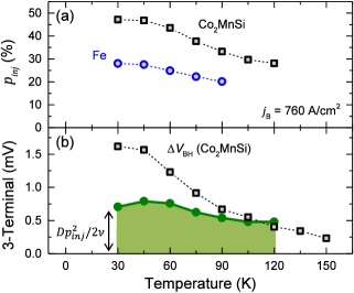
We determine the spin accumulation profile in the channel by discretizing the standard spin drift-diffusion relations in three dimensions and solving for the average injector polarization which upon Laplace relaxation yields the experimentally observed EMF111See Supplemental Material at [URL from Publisher] for calculation details.. Fig. 4(a) shows as a function of temperature for both a Co2MnSi device () and an Fe device (). Notably, these values were obtained solely from bulk semiconductor parameters and are independent of any assumptions about the efficiency of spin-dependent tunneling at the heterojuctions.
The experimental temperature dependence of the three-terminal signal is shown in Fig. 4(b), where injector contact B also functions as a polarized detector. The magnitude of the three-terminal Hanle signal may be decomposed as . The first term originates from the usual spin-dependence of the interfacial tunneling conductance. The second term represents a hitherto unconsidered contribution from the spin-generated EMF as a shift of the average electrochemical potential. The green shaded region in Fig. 4(b) indicates the magnitude of this contribution as determined from the polarization values in Fig. 4(a). The spin-generated EMF constitutes a significant fraction of the three-terminal signal across the entire temperature range. This contribution must therefore be taken into account when interpreting ferromagnetic detection signals in the regime of large spin polarization.
In conclusion, we have experimentally demonstrated the presence of an EMF which must accompany a spin accumulation in steady-state due to a non-constant density of states and population imbalance of the two spin sub-bands. The close analogy with thermoelectric physics suggests the possibility of observing a class of related effects in which the source of the deviation from equilibrium in free energy density is spin rather than heat. Since the behavior of this phenomenon may be parameterized by independent measurements, the spin accumulation in the channel may be identified unambiguously and quantified in absolute terms. This represents an attractive detection alternative in situations where traditional ferromagnetic techniques are either unfeasible or unreliable.
This work was supported by NSF Grant No. DMR-1104951; by C-SPIN, one of the six centers of STARnet, a Semiconductor Research Corporation program sponsored by MARCO and DARPA; and by the NSF MRSEC program. Parts of this work were carried out in the Minnesota Nano Center which receives partial support from NSF through the NNIN program.
References
- Lou et al. (2007) X. Lou, C. Adelmann, S. A. Crooker, E. S. Garlid, J. Zhang, K. S. M. Reddy, S. D. Flexner, C. J. Palmstrøm, and P. A. Crowell, Nature Phys. 3, 197 (2007).
- Ciorga et al. (2009) M. Ciorga, A. Einwanger, U. Wurstbauer, D. Schuh, W. Wegscheider, and D. Weiss, Phys. Rev. B 79, 165321 (2009).
- Salis et al. (2011) G. Salis, S. F. Alvarado, and A. Fuhrer, Phys. Rev. B 84, 041307 (2011).
- Uemura et al. (2011) T. Uemura, T. Akiho, M. Harada, K.-i. Matsuda, and M. Yamamoto, Appl. Phys. Lett. 99, 082108 (2011).
- van ’t Erve et al. (2007) O. M. J. van ’t Erve, A. T. Hanbicki, M. Holub, C. H. Li, C. Awo-Affouda, P. E. Thompson, and B. T. Jonker, Appl. Phys. Lett. 91, 212109 (2007).
- Appelbaum et al. (2007) I. Appelbaum, B. Huang, and D. J. Monsma, Nature 447, 295 (2007).
- Dash et al. (2009) S. P. Dash, S. Sharma, R. S. Patel, M. P. de Jong, and R. Jansen, Nature 462, 491 (2009).
- Suzuki et al. (2011) T. Suzuki, T. Sasaki, T. Oikawa, M. Shiraishi, Y. Suzuki, and K. Noguchi, Appl. Phys. Express 4, 023003 (2011).
- Jansen et al. (2012) R. Jansen, S. P. Dash, S. Sharma, and B. C. Min, Semicond. Sci. Technol. 27, 083001 (2012).
- Tombros et al. (2007) N. Tombros, C. Jozsa, M. Popinciuc, H. T. Jonkman, and B. J. van Wees, Nature 448, 571 (2007).
- Zhou et al. (2011) Y. Zhou, W. Han, L.-T. Chang, F. Xiu, M. Wang, M. Oehme, I. A. Fischer, J. Schulze, R. K. Kawakami, and K. L. Wang, Phys. Rev. B 84, 125323 (2011).
- Saito et al. (2013) T. Saito, N. Tezuka, M. Matsuura, and S. Sugimoto, Appl. Phys. Lett. 103, 122401 (2013).
- Manzke et al. (2013) Y. Manzke, R. Farshchi, P. Bruski, J. Herfort, and M. Ramsteiner, Phys. Rev. B 87, 134415 (2013).
- Akiho et al. (2013) T. Akiho, J. Shan, H.-x. Liu, K.-i. Matsuda, M. Yamamoto, and T. Uemura, Phys. Rev. B 87, 235205 (2013).
- Han et al. (2013) W. Han, X. Jiang, A. Kajdos, S.-H. Yang, S. Stemmer, and S. S. P. Parkin, Nature Communications 4, 1 (2013).
- Valenzuela and Tinkham (2006) S. O. Valenzuela and M. Tinkham, Nature 442, 176 (2006).
- Olejník et al. (2012) K. Olejník, J. Wunderlich, A. C. Irvine, R. P. Campion, V. P. Amin, J. Sinova, and T. Jungwirth, Phys. Rev. Lett. 109, 076601 (2012).
- Yu and Flatté (2002) Z. G. Yu and M. E. Flatté, Phys. Rev. B 66, 235302 (2002).
- Vera-Marun et al. (2011) I. J. Vera-Marun, V. Ranjan, and B. J. van Wees, Phys. Rev. B 84, 241408 (2011).
- Vera-Marun et al. (2012) I. J. Vera-Marun, V. Ranjan, and B. J. van Wees, Nature Phys. 8, 313 (2012).
- Paget (1981) D. Paget, Phys. Rev. B 24, 3776 (1981).
- Kölbl et al. (2012) D. Kölbl, D. M. Zumbühl, A. Fuhrer, G. Salis, and S. F. Alvarado, Phys. Rev. Lett. (2012).
- Chan et al. (2009) M. K. Chan, Q. O. Hu, J. Zhang, T. Kondo, C. J. Palmstrøm, and P. A. Crowell, Phys. Rev. B 80, 161206 (2009).
- Paget et al. (1977) D. Paget, G. Lampel, B. Sapoval, and V. I. Safarov, Phys. Rev. B 15, 5780 (1977).
- Crooker et al. (2009) S. A. Crooker, E. S. Garlid, A. N. Chantis, D. L. Smith, K. S. M. Reddy, Q. O. Hu, T. Kondo, C. J. Palmstrøm, and P. A. Crowell, Phys. Rev. B 80, 041305 (2009).
- Ashcroft and Mermin (1976) N. W. Ashcroft and N. D. Mermin, Solid State Physics (Holt, Rinehart and Winston, New York, 1976).
- Johnson and Lark-Horovitz (1953) V. A. Johnson and K. Lark-Horovitz, Physical Review 92, 226 (1953).
- Smith (1978) R. A. Smith, Semiconductors, 2nd ed. (Cambridge University Press, New York, 1978).
- Isenberg et al. (1948) I. Isenberg, B. R. Russell, and R. F. Greene, Rev. Sci. Instrum. 19, 685 (1948).
- Note (1) See Supplemental Material at [URL from Publisher] for calculation details.