Enhanced absorption of monolayer MoS2 with resonant back reflector
Abstract
By extracting the permittivity of monolayer MoS2 from experiments, the optical absorption of monolayer MoS2 prepared on top of one-dimensional photonic crystal (1DPC) or metal films is investigated theoretically. The 1DPC and metal films act as resonant back reflectors that can enhance absorption of monolayer MoS2 substantially over a broad spectral range due to the Fabry-Perot cavity effect. The absorption of monolayer MoS2 can also be tuned by varying either the distance between the monolayer MoS2 and the back reflector or the thickness of the cover layers.
Jiang-Tao Liu,1,2,∗ Tong-Biao Wang,2 Xiao-Jing Li,3 and Nian-Hua Liu1,2
1Nanoscale Science and Technology Laboratory, Institate for Advanced Study, Nanchang University, Nanchang 330031, China
2Department of Physics, Nanchang University, Nanchang 330031, China
3College of Physics and Energy, Fujian Normal University, Fuzhou 350007, China
∗Corresponding author: jtliu@semi.ac.cn
Monolayer MoS2 as a new kind of two dimensional (2D) semiconductor has elicited significant attention because of its distinctive electronic and optical properties [1, 2, 3, 4, 5, 6, 7, 8, 9, 10, 11, 12, 13, 14]. Monolayer MoS2 exhibits a direct band gap in the visible frequency range [1, 2, 3, 4], which is more favorable for optoelectronic applications than graphene in numerous cases. Monolayer MoS2 has show numerous potential applications in flexible phototransistors, photodetectors, photovoltaics, and signal amplification [5, 6, 7, 8, 9, 10, 11, 12, 13]. Notably, the photoresponsivity of monolayer MoS2 photodetectors can reach 880 A/W, which is 106 better than that of the first graphene photodetectors (0.5 mA/W) [5].
The optical absorbance in monolayer MoS2 is minimal () due to its ultrathin thickness, which is not conducive to fabrication of photodetectors, solar cells, and optical amplification. Thus, to promote the applications of monolayer MoS2, the optical absorptance in monolayer MoS2 waves should be enhanced. In studies of graphene, several mechanisms have been proposed to enhance the absorption of graphene, e.g., periodically patterned graphene, surface plasmon, microcavity, graphene-negative permittivity metamaterials, and attenuated total reflectance, etc [15, 16, 17, 18, 19, 20, 21, 22, 23]. The interaction between graphene and optical beams can also be enhanced when the graphene layers are prepared on top of one-dimensional photonic crystal (1DPC) or with resonant metal back reflectors because of the Fabry-Perot (F-P) cavity effect [24, 25, 26]. The proposed structures are very easy to fabricate using existing technology.
In this Letter, the optical absorption of monolayer MoS2 prepared on top of 1DPC or metal films with a spacer layer and cover layers is investigated theoretically. We find that the absorption of monolayer MoS2 can be enhanced by nearly four times because of the F-P interference. The absorption of monolayer MoS2 with 1DPC is slight larger than that of monolayer MoS2 with metal films. However, the full width at half maximum (FWHM) of the absorption spectrum of monolayer MoS2 with metal films is much larger than that of monolayer MoS2 on top of 1DPC. The absorption of monolayer MoS2 can also be tuned by varying the thickness of spacer layers and cover layers. Our proposal is very easy to implement and has potential important applications in monolayer MoS2 optoelectronic devices.
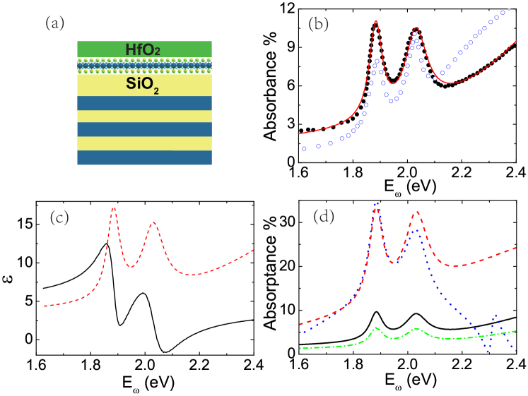
The details of the structure are shown in the inset of Fig. 1 (a). The 0.65 nm monolayer MoS2 is prepared on top of the SiO2 spacer layer with high- dielectric HfO2 cover layers. A 1DPC or 130 nm silver film is placed at the bottom of the SiO2 spacer layer as the resonant back reflector (RBR). The 1DPC is composed of alternating MgF2 and ZnS layers with a total of 8.5 periods. The permittivity for silver film is frequency dependent [27]. The refractive indices of SiO2, HfO2, MgF2, and ZnS at nm are , , , and , respectively [27].
To model the absorption of monolayer MoS2 in these structures, the details of the permittivity of monolayer MoS2 must be obtained first. Numerous methods based on first-principle calculations have been used in the calculations of the optical spectrum of monolayer MoS2 [28, 29, 30, 31]. However, the reported theory results are conflicting. Differences between theoretical results and experiment results have been noted. The permittivity of monolaye MoS2 can be extracted from experiments with the use of two exciton transition and the band transition [2]. The imaginary permittivity of exciton can be described by Lorentzian function. Neglecting the variation of the transition matrix elements with energy, the band absorption of a 2D semiconductor can be described by the step function and the corresponding imaginary permittivity is , where is the speed of light in vacuum and is the transverse component of the static refractive index [30]. Thus, the imaginary part of the total permittivity can be expressed as
| (1) | |||||
where (), (), and () are the linewidth, equivalent oscillator strength, and transition energy of A (B) excitons, respectively, is the band gap of monolayer MoS2, is the equivalent oscillator strength of interband transition, is the step function with a broadening of , where is the linewidth of the interband transition. The spin-orbit splitting is negligible in the band absorption because spin-orbit splitting is much smaller than the band gap. The real part of the permittivity of monolayer MoS2 can be obtained using Kramers-Kronig relations
| (2) |
where is the principal value integral.
The parameters in Eq. (1) are obtained by fitting the experimental data using the standard transfer matrix method [24]. The results are shown in Table 1 and Fig. 1(b). Although nine fitting parameters are in Eq. (1), these parameters are relatively independent. For instance, the parameters , , and are decided by the absorption peak located at about 1.88 eV. However, the parameters , , and are obtained by fitting the absorption peak located at 2.02 eV. The linewidth of the band transition is much larger than that of the traditional semiconductor quantum well, which may have been caused by the strong coulomb interaction and the strong electron-phonon interaction. The folds of monolayer MoS2 and the interaction with the substrate may also enhance the linewidth. The fitting of the absorption spectra is small, which indicates that it is mainly contributed by the quasiparticle band absorption.
| 1.884 eV | 28 meV | 2.02 eV | 42 meV | 0.32 eV |
| 0.43 eV | 2.43 eV | 0.398 eV | 59 |
The monolayer MoS2 has a large imaginary part of permittivity [Fig. 1(c)]. However, the maximum absorptance (i.e., the directly proportional ratio of the radiation absorbed by the monolayer MoS2 to that incident upon it) of suspended monolayer MoS2 is only about 9.6% due to its ultrathin thickness. By contrast, when a monolayer MoS2 is prepared on top of the 1DPC (silver film), the maximum absorptance can be as high as 34.9% (33.5%)[Fig. 1(c)]. Thus, the absorptance of monolayer MoS2 with 1DPC (silver) film can be enhanced by about 3.64 (3.49) times. In this structures, the monolayer MoS2 and the RBR act as the mirrors of the F-P cavity. The light propagates back and forth in the F-P cavity, which enhances the absorption of monolayer MoS2. The maximum absorption of monolayer MoS2 with 1DPC is slightly larger than that of monolayer MoS2 with a silver film due to the higher reflectivity of 1DPC. However, the reflectivity of 1DPC is limited to the photonic band gap width in 1DPC. By contrast, the silver film can reflect lights effectively within the visible light range. Thus, the FWHM of the absorption spectrum of monolayer MoS2 with silver film is much larger than that of monolayer MoS2 with 1DPC. To contrast, we also show the absorptance of the monolayer MoS2 prepared on top of thick SiO2 substrate in fig. 1(d). The maximum absorptance is only about 6.1%, which is smaller than that of suspended monolayer MoS2 due to that the traditional substrate material enhance the reflection of the monolayer MoS2.
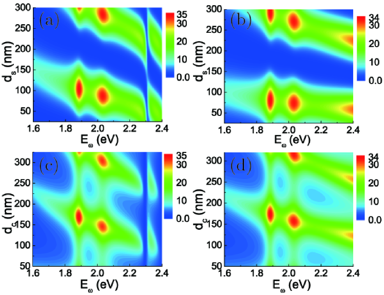
The absorption of monolayer MoS2 can also be tuned by varying the thickness of the spacer layer. In Figs. 2(a) and 2(b), we plot the absorptance of monolayer MoS2 as a function of the wavelength and the spacer layers thickness without cover layers. Similar to the microcavity, the resonant absorption wavelength of monolayer MoS2 with 1DPC can be described as with including the half-wave loss, where m is an integer. Thus, the absorption peak photon energy increases with decreasing spacer layer thickness. However, the resonant absorption wavelength of monolayer MoS2 with silver films is not strictly equal to duo to the dispersion and existing skin depth in the silver films. The absorption peak photon energy of monolayer MoS2 with silver films increases slowly with decreasing spacer layer thickness. The electron mobility in monolayer MoS2 can be enhanced several times by the high- dielectric HfO2 cover layers [32, 33]. The cover layers can also adjust the absorption of monolayer MoS2. The details are shown in Figs. 2(c) and 2(d). The normal cover layers cannot enhance the absorptance of monolayer MoS2. However, the peak photon energy can be tuned by varying the thickness of the cover layers. Different from the spacer layer, the absorption of monolayer MoS2 with both 1DPC and silver films are the same way when the cover layer thickness increases.
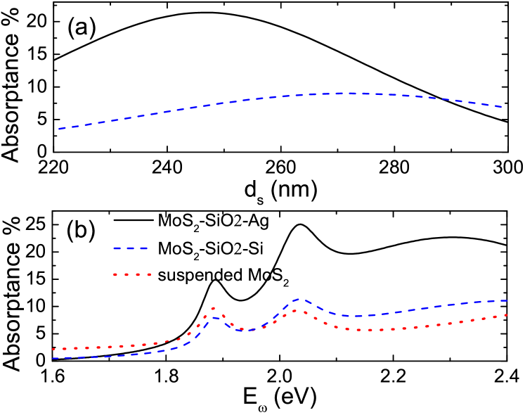
Finally, we turn to the discussion on the absorptance of the monolayer MoS2 prepared on top of Si substrate with SiO2 spacer layer. This structure has been fabricated in the experiment [5]. The Si substrate can also act as the RBR due to its high refractive index, and thus enhance the absorptance of the monolayer MoS2. The absorptance of the monolayer MoS2 with Si substrate as function of the spacer layers thickness for optical wavelength (same as in the experiment [5]). For nm, the maximum absorptance of the monolayer MoS2 is about 9% [Fig. 3(a)]. This is why a nm SiO2 spacer layer is fabricated in experiment. By contrast, the absorptance of suspended monolayer MoS2 is about 5.9% and the absorptance of monolayer MoS2 with sliver films is about 22% due to the higher reflectivity of sliver films. Furthermore, the FWHM of the absorption spectrum of monolayer MoS2 with metal films is larger than that of monolayer MoS2 with Si substrate [Fig. 3(b)]. Thus if the Si substrate is replaced by the metal films in the experiment, the photoresponsivity and the FWHM of monolayer MoS2 photodetectors can be further enhanced greatly.
In conclusion, the optical absorption of monolayer MoS2 prepared on top of 1DPC or silver films with a spacer layer is investigated theoretically. In these structures, the maximum optical absorptance of monolayer MoS2 can be raised to 35% with a large FWHM due to the F-P cavity effect. The absorption of monolayer MoS2 with 1DPC is slightly larger than that of monolayer MoS2 with silver films. However, the FWHM of the absorption spectrum of monolayer MoS2 with silver film is much larger than that of monolayer MoS2 with 1DPC. The absorption of monolayer MoS2 can also be tuned by varying the thickness of the spacer layers and cover layers. Our proposal is very easy to implement and may have potentially important applications in the development of monolayer MoS2 based optoelectronic devices.
This work was supported by the NSFC Grant Nos. 11264029, 11264030, and 11364033, the NSF from the Jiangxi Province No. 20122BAB212003.
Added Materials
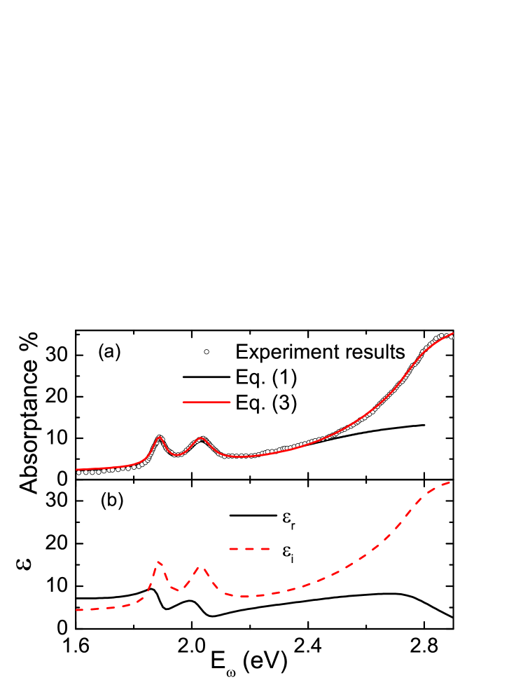
In the front section, the permittivity of monolayer MoS2 is extracted from experiment results[2]. In Ref. [2], experimental measurement is in the range about 1.6-2.4 eV. In the Fig. 2(d) in Ref. [28], a experiment result of the absorption monolayer MoS2 in the range about 1.6-2.9 eV is present. Next, we extract The permittivity of monolaye MoS2 in the range about 1.6-2.9 eV from the Fig. 2(d) in Ref. [28]. Similar Eq. (1) but using two band transition, the imaginary part of the total permittivity can be expressed as
| (3) | |||||
where (), (), and () are equivalent oscillator strength of interband transition, the linewidth, band gap, and linewidth of the interband transition of A (B) band, respectively, , meV is used in the calculation. The real part of the permittivity of monolayer is obtained by using Eq. (2). is adjusted to make (if the real part of the permittivity is not too large, the absorption of the monolayer MoS2 is only depended on the imaginary part of the permittivity). To compare with the experiment results, the absorbance of monolayer MoS2 is calculated by using the same method as in Refs. [2] and [34].
Results are shown in Fig. 4 and table 3 (at the last page of the paper). Compared with results in table 1, a little changes of the parameters of A and B exicitons can be found. However, the parameters of the band transition fitted by Eq. (3) is different with that fitted by using Eqs. (1).
| 1.887 eV | 28 meV | 2.03 eV | 46 meV |
| 0.29 eV | 0.40 eV | 2.60 eV | |
| 74 | 50 | 244 meV | 82 meV |
References
- [1] Q. H. Wang, K. Kalantar-Zadeh, A. Kis, J. N. Coleman, and M. S. Strano, Nat. Nanotech. 7, 699 (2012).
- [2] K. F. Mak, C. Lee, J. Hone, J. Shan, and T. F. Heinz, Phys. Rev. Lett. 105, 136805 (2010).
- [3] A. Splendiani, L. Sun, Y. Zhang, T. Li, J. Kim, C. Y. Chim, G. Galli, and F. Wang, Nano Lett. 10, 1271 (2010).
- [4] T. Li and G. Galli, J. Phys. Chem. C 111, 16192 (2007).
- [5] O. Lopez-Sanchez, D. Lembke, M. Kayci, A. Radenovic, and A. Kis, Nat. Nanotech. 8, 497 (2013).
- [6] Z. Yin, H. Li, H. Li, L. Jiang, Y. Shi, Y. Sun, G. Lu, Q. Zhang, X. Chen, and H. Zhang, ACS Nano 6, 74 (2011).
- [7] H. S. Lee, S. W. Min, Y. G. Chang, M. K. Park, T. Nam, H. Kim, J. H. Kim, S. Ryu, and S. Im, Nano Lett. 12, 3695 (2012).
- [8] W. Choi, M. Y. Cho, A. Konar, J. H. Lee, G. Cha, S. C. Hong, S. Kim, J. Kim, D. Jena, J. Joo, and S. Kim, Adv. Mater. 24, 5832 (2012).
- [9] M. Bernardi, M. Palummo, and J. C. Grossman, Nano Lett. 13, 3664 (2013).
- [10] J. Pu, Y. Yomogida, K. K. Liu, L. J. Li, Y. Iwasa, and T. Takenobu, Nano Lett. 12, 4013 (2012).
- [11] C. Janisch, N. Mehta, D. Ma, A. L. El as, N. Perea-L pez, M. Terrones, and Z. Liu, Opt. Lett. 39, 383 (2014).
- [12] A. Sobhani, A. Lauchner, S. Najmaei, C. Ayala-Orozco, F. Wen, J. Lou, and N. J. Halas, Appl. Phys. Lett. 104, 031112 (2014).
- [13] X. Gan, Y. Gao, K. F. Mak, X. Yao, R. J. Shiue, A. van der Zande, M. E. Trusheim, F. Hatami, T. F. Heinz, J. Hone, and D. Englund, Appl. Phys. Lett. 103, 181119 (2013).
- [14] Y. V. Bludov, M. I. Vasilevskiy, and N. M. R. Peres, J. Appl. Phys. 112, 084320 (2012).
- [15] S. Thongrattanasiri, F. H. L. Koppens, and F. J. G. de Abajo, Phys. Rev. Lett. 108, 047401 (2012).
- [16] A. Ferreira, N. M. R. Peres, R. M. Ribeiro, and T. Stauber, Phys. Rev. B 85, 115438 (2012).
- [17] M. A. Vincenti, D. de Ceglia, M. Grande, A. D’Orazio, and M. Scalora, Opt. Lett. 38, 3550 (2013).
- [18] A. Ferreira and N. M. R. Peres, Phys. Rev. B 86, 205401 (2012).
- [19] Z. Z. Zhang, K. Chang, and F. M. Peeters, Phys. Rev. B 77, 235411 (2008).
- [20] W. Zhao, K. Shi, and Z. Lu, Opt. Lett. 38, 4342 (2013).
- [21] Q. Ye, J. Wang, Z. Liu, Z. C. Deng, X. T. Kong, F. Xing, X. D. Chen, W. Y. Zhou, C. P. Zhang, and J. G. Tian, Appl. Phys. Lett 102, 021912 (2013).
- [22] R. Alaee, M. Farhat, C. Rockstuhl, and F. Lederer, Optics Express 20, 28017 (2012).
- [23] X. Zhu, W. Yan, P. U. Jepsen, O. Hansen, N. A. Mortensen, and S. Xiao, Appl. Phys. Lett. 102, 131101 (2013).
- [24] J. T. Liu, N. H. Liu, J. Li, X. J. Li, and J. H. Huang, Appl. Phys. Lett 101, 052104 (2012).
- [25] N. M. R. Peres and Y. V. Bludov, EPL 101, 58002 (2013).
- [26] J. T. Liu, N. H. Liu, L. Wang, X. H. Deng, and F. H. Su, EPL 104, 57002 (2013).
- [27] E. D. Palik, ed., Handbook of Optical Constants of Solids (Academic Press, Boston, 1985).
- [28] D. Y. Qiu, F. H. da Jornada, and S. G. Louie, Phys. Rev. Lett. 111, 216805 (2013).
- [29] H. Shi, H. Pan, Y. W. Zhang, and B. I. Yakobson, Phys. Rev. B 87, 155304 (2013).
- [30] T. Cheiwchanchamnangij and W. R. L. Lambrecht, Phys. Rev. B 85, 205302 (2012).
- [31] A. Ramasubramaniam, Phys. Rev. B 86, 115409 (2012).
- [32] B. Radisavljevic, A. Radenovic, J. Brivio, V. Giacometti, and A. Kis, Nat. Nanotech. 6, 147 (2011).
- [33] Y. Yoon, K. Ganapathi, and S. Salahuddin, Nano Lett. 11, 3768 (2011).
- [34] Kin Fai Mak, Matthew Y. Sfeir, Yang Wu, Chun Hung Lui, James A. Misewich, and Tony F. Heinz, Phys. Rev. Lett. 101, 196405 (2008).
| (eV) | (eV) | (eV) | ||||||
|---|---|---|---|---|---|---|---|---|
| 1.60 | 7.17 | 4.43 | 2.04 | 4.01 | 14.29 | 2.48 | 7.26 | 12.61 |
| 1.61 | 7.16 | 4.46 | 2.05 | 3.39 | 13.32 | 2.49 | 7.34 | 12.94 |
| 1.62 | 7.16 | 4.48 | 2.06 | 3.05 | 12.14 | 2.50 | 7.42 | 13.29 |
| 1.63 | 7.15 | 4.51 | 2.07 | 2.95 | 11.03 | 2.51 | 7.49 | 13.65 |
| 1.64 | 7.16 | 4.54 | 2.08 | 2.99 | 10.11 | 2.52 | 7.56 | 14.02 |
| 1.65 | 7.16 | 4.58 | 2.09 | 3.11 | 9.39 | 2.53 | 7.63 | 14.40 |
| 1.66 | 7.17 | 4.61 | 2.10 | 3.27 | 8.85 | 2.54 | 7.69 | 14.79 |
| 1.67 | 7.18 | 4.65 | 2.11 | 3.44 | 8.45 | 2.55 | 7.75 | 15.20 |
| 1.68 | 7.20 | 4.70 | 2.12 | 3.61 | 8.15 | 2.56 | 7.81 | 15.62 |
| 1.69 | 7.23 | 4.74 | 2.13 | 3.78 | 7.94 | 2.57 | 7.87 | 16.06 |
| 1.70 | 7.26 | 4.79 | 2.14 | 3.94 | 7.79 | 2.58 | 7.92 | 16.50 |
| 1.71 | 7.29 | 4.85 | 2.15 | 4.09 | 7.69 | 2.59 | 7.97 | 16.96 |
| 1.72 | 7.33 | 4.91 | 2.16 | 4.23 | 7.62 | 2.60 | 8.01 | 17.44 |
| 1.73 | 7.38 | 4.98 | 2.17 | 4.36 | 7.59 | 2.61 | 8.05 | 17.92 |
| 1.74 | 7.44 | 5.06 | 2.18 | 4.48 | 7.58 | 2.62 | 8.09 | 18.43 |
| 1.75 | 7.51 | 5.15 | 2.19 | 4.60 | 7.59 | 2.63 | 8.13 | 18.95 |
| 1.76 | 7.59 | 5.26 | 2.20 | 4.72 | 7.62 | 2.64 | 8.16 | 19.50 |
| 1.77 | 7.68 | 5.38 | 2.21 | 4.83 | 7.66 | 2.65 | 8.19 | 20.07 |
| 1.78 | 7.79 | 5.53 | 2.22 | 4.93 | 7.72 | 2.66 | 8.22 | 20.66 |
| 1.79 | 7.92 | 5.72 | 2.23 | 5.04 | 7.79 | 2.67 | 8.24 | 21.29 |
| 1.80 | 8.07 | 5.95 | 2.24 | 5.14 | 7.87 | 2.68 | 8.25 | 21.95 |
| 1.81 | 8.25 | 6.24 | 2.25 | 5.23 | 7.96 | 2.69 | 8.25 | 22.65 |
| 1.82 | 8.46 | 6.63 | 2.26 | 5.33 | 8.06 | 2.70 | 8.23 | 23.40 |
| 1.83 | 8.70 | 7.18 | 2.27 | 5.42 | 8.17 | 2.71 | 8.19 | 24.18 |
| 1.84 | 8.97 | 7.95 | 2.28 | 5.52 | 8.28 | 2.72 | 8.12 | 25.01 |
| 1.85 | 9.23 | 9.09 | 2.29 | 5.61 | 8.41 | 2.73 | 8.02 | 25.86 |
| 1.86 | 9.38 | 10.78 | 2.30 | 5.70 | 8.54 | 2.74 | 7.87 | 26.73 |
| 1.87 | 9.16 | 13.09 | 2.31 | 5.79 | 8.69 | 2.75 | 7.68 | 27.60 |
| 1.88 | 8.15 | 15.39 | 2.32 | 5.88 | 8.84 | 2.76 | 7.44 | 28.44 |
| 1.89 | 6.45 | 16.02 | 2.33 | 5.97 | 9.00 | 2.77 | 7.17 | 29.24 |
| 1.90 | 5.09 | 14.46 | 2.34 | 6.06 | 9.17 | 2.78 | 6.86 | 29.98 |
| 1.91 | 4.61 | 12.30 | 2.35 | 6.15 | 9.35 | 2.79 | 6.53 | 30.66 |
| 1.92 | 4.68 | 10.68 | 2.36 | 6.24 | 9.54 | 2.80 | 6.17 | 31.27 |
| 1.93 | 4.97 | 9.69 | 2.37 | 6.33 | 9.73 | 2.81 | 5.81 | 31.81 |
| 1.94 | 5.31 | 9.19 | 2.38 | 6.42 | 9.94 | 2.82 | 5.44 | 32.30 |
| 1.95 | 5.65 | 9.04 | 2.39 | 6.51 | 10.16 | 2.83 | 5.07 | 32.72 |
| 1.96 | 5.97 | 9.17 | 2.40 | 6.59 | 10.38 | 2.84 | 4.71 | 33.10 |
| 1.97 | 6.24 | 9.55 | 2.41 | 6.68 | 10.62 | 2.85 | 4.34 | 33.43 |
| 1.98 | 6.46 | 10.16 | 2.42 | 6.77 | 10.87 | 2.86 | 3.98 | 33.71 |
| 1.99 | 6.58 | 11.03 | 2.43 | 6.85 | 11.13 | 2.87 | 3.63 | 33.97 |
| 2.00 | 6.54 | 12.12 | 2.44 | 6.94 | 11.40 | 2.88 | 3.29 | 34.19 |
| 2.01 | 6.24 | 13.30 | 2.45 | 7.02 | 11.69 | 2.89 | 2.95 | 34.39 |
| 2.02 | 5.65 | 14.27 | 2.46 | 7.10 | 11.98 | 2.90 | 2.62 | 34.56 |
| 2.03 | 4.83 | 14.67 | 2.47 | 7.19 | 12.29 |