One-dimensional Silicon and Germanium Nanostructures With No Carbon Analogues
E. Perim ∗ a, R. Paupitz b, T. Botari a and D. S. Galvaoa
a Instituto de Física ‘Gleb Wataghin’, Universidade Estadual de Campinas, 13083-970, Campinas, SP, Brazil.
b Departamento de Física - Universidade Estadual Paulista Av.24A 1515 - 13506-900 - Rio Claro - SP - Brazil.
∗ Corresponding author: eric.perim@gmail.com
In this work we report new silicon and germanium tubular nanostructures with no corresponding stable carbon analogues. The electronic and mechanical properties of these new tubes were investigated through ab initio methods. Our results show that the structures have lower energy than their corresponding nanoribbon structures and are stable up to high temperatures (500 and 1000 K, for silicon and germanium tubes, respectively). Both tubes are semiconducting with small indirect band gaps, which can be significantly altered by both compressive and tensile strains. Large bandgap variations of almost were observed for strain rates as small as , suggesting possible applications in sensor devices. They also present high Young’s modulus values (0.25 and 0.15 TPa, respectively). TEM images were simulated to help the identification of these new structures.
I Introduction
Carbon nanostructures present very interesting electronic and mechanical properties. The discovery of fullerenes Kroto et al. (1985), carbon nanotubes Iijima (1991), and more recently graphene Novoselov et al. (2004), has created a new era in materials science. In particular, the discovery of new and very unusual graphene properties has led to a renewed interest in the search for other similar structures.
A natural question is whether other atoms in the same column of the periodic table as carbon (such as, silicon and germanium) could produce similar structures. This has motivated many studies Röthlisberger et al. (1994); Takeda and Shiraishi (1994); Zunger and Wang (1996); Singh et al. (2004), which produced important results. It has been demonstrated that silicon and germanium are able to produce many analogues of the carbon nanostructures, such as closed cage structures Röthlisberger et al. (1994), nanotubes Singh et al. (2004); Fagan et al. (2000); Guo et al. (2012); Bai et al. (2004); Sha et al. (2002); Zhang et al. (2002); Durgun et al. (2005); Pradhan and Ray (2006), and even two-dimensional honeycomb graphene-like sheets Takeda and Shiraishi (1994); Cahangirov et al. (2009); Topsakal and Ciraci (2010); Zhao (2012); Botari et al. (2014), the so-called silicene and germanene, which have been already experimentally realized Ni et al. (2011); O’hare et al. (2012); Vogt et al. (2012); Dávila et al. (2014). More recently, multilayer silicene has been synthesized and shown to be promising for electronic applications Vogt et al. (2014) as well as stable under ambient conditions Padova et al. (2014).
However, despite all these similarities, there are important and significant differences among carbon and silicon and/or germanium structures. Due to the pseudo Jahn-Teller effect (PJTE) Hobey (1965); Jose and Datta (2012); Bersuker (2013), silicon and germanium nanostructures tend to form buckled geometries, as a consequence of a stronger character, in comparison to carbon ones. Structural buckling of both silicene and germanene structures has been already demonstrated Cahangirov et al. (2009). In principle, due to these differences, it is possible that unique silicon and germanium structures can exist, with no corresponding carbon counterpart. In this work we report new one-dimensional silicon and germanium nanostructures, with no corresponding stable carbon analogues. Not only these structures break the usual analogy, they are also mechanically robust and present promising electronic properties for technological applications.
II Methodology
The structural, electronic and mechanical properties of these new structures were investigated through ab initio density functional theory (DFT) methods using the DMol Delley (2000) package, as implemented in the Accelrys Materials Studio Suite. The DFT calculations were carried out in the generalized gradient approximation (GGA), with the Perdew-Burke-Ernzerhof (PBE) Perdew et al. (1996) functional for exchange-correlation terms. All calculations were carried with double-numeric quality basis set with polarization function and all-electron core treatment. Geometric optimizations were carried out with a tolerance of Ha in energy, 0.002 Ha/Å in force and 0.005Å in spatial displacement with full cell parameter optimizations. A k-point grid of 5x1x1 was used, yielding a separation of Å-1 between k-points in the reciprocal space. The molecular dynamics (MD) simulations were performed under the Born-Oppenheimer aproximation in a NVT ensemble, with time steps of 1.0fs and massive generalized gaussian moments (GGM) thermostat with Nosé chain length of 2 and a Yoshida parameter Delley (2000) of 3 for a simulation time of 5ps.
III Results and Discussion
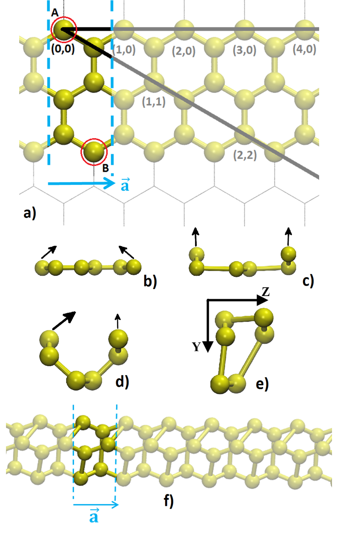
The new proposed silicon and germanium nanotubes are presented in Figure 1. These are the smallest possible nanotubes which can be formed from a two-ring wide zigzag nanoribbon structure. One unique aspect of these tubes is that they present no helicity despite being neither armchair or zigzag (see Figure 1 (a)). These structures can be generated moving the three atomic chains that compose the nanoribbon into a tubular configuration (see Figure 1) with six atoms in the unit cell. The transverse dimensions along the directions y and z specified in Figure 1 are, respectively, 6.36Å and 4.69Å for the Si tube and 6.98Å and 5.15Å for the Ge tube.
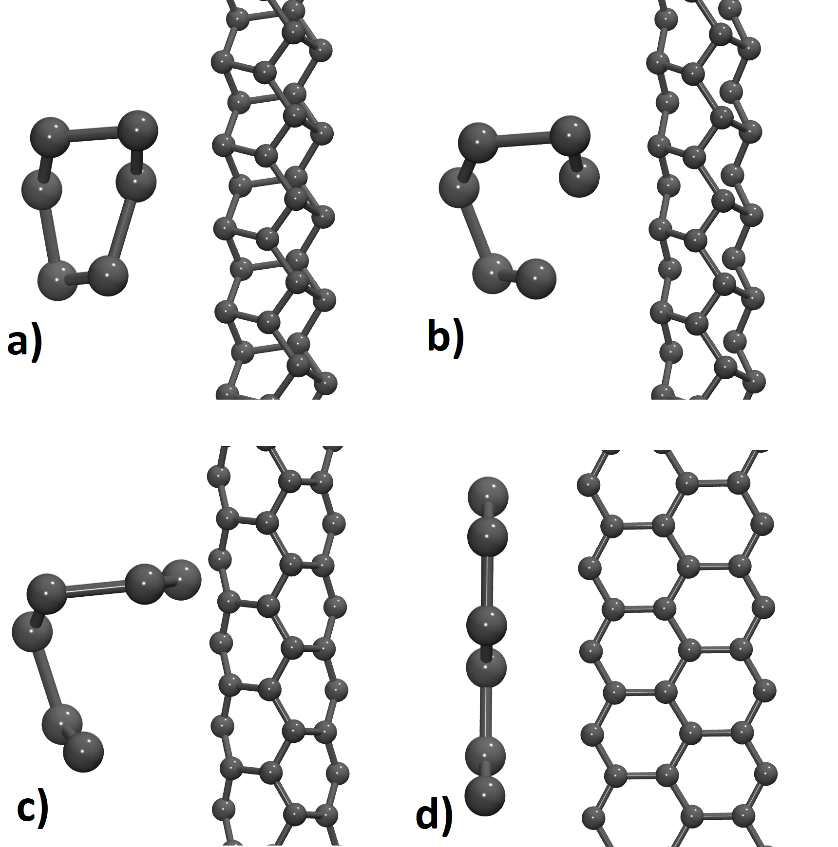
No stable carbon structure can be formed with this morphology, the simulations showed it collapses into its planar nanoribbon conformation. Successive snapshots of the carbon nanotube optimization process are shown in Figure 2, depicting the transition from the tubular structure, which has a partial character, to the planar and purely nanoribbon. To understand why these silicon and germanium structures are stable while the carbon one is not, we must consider the pseudo Jahn-Teller Effect (PJTE) Hobey (1965); Jose and Datta (2012); Bersuker (2013). Since silicon and germanium orbitals are much closer in energy than the corresponding carbon ones Jose and Datta (2012), the PJTE is much stronger in silicon and germanium structures than on their carbon counterparts. This is reflected into a stronger hybridization character, which favors and stabilizes the -like tubular structures. In the carbon case, since the hybridization is favored (and more stable), the small-diameter tubular structures become unstable. The manifestation of the PJTE in these aspects is very interesting, as it breaks the usual structural analogy between carbon and silicon or germanium, leading to the existence of stable nanostructures with no carbon analogues. The silicon and germanium tubes are thermally stable up to temperatures of 500 and 1000 K, respectively. See Supplemental Material for a video showing successive geometry optimization cycles of the C tube, depicting the transition from the tubular morphology to the nanoribbon.
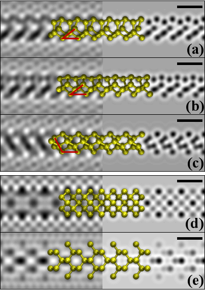
In order to facilitate their possible identification, we simulated transmission electron microscopy (TEM) images of the structures and compared them with an image of a very thin silicon nanowire grown along the (1 0 0) direction. This comparison is shown in Figure 3. The TEM images were generated using the QSTEM software Koch (2002) with a voltage of 200kV, Scherzer defocus and two different values for the spherical aberration, 0.5mm and 0.005mm, trying to emulate a more conventional microscope and a higher end one, respectively. We speculate that such structures could be observed as a result of experiments similar to those performed by Takayanagi et al. Ohnishi et al. (1998), Lou et al. Lu et al. (2010), Yacaman et al. Troiani et al. (2003) or Ajayan and IIjima Ajayan and Iijima (1992), where strain is used to induce the formation of one-dimensional structures. Considering the recent efforts on the production of silicene and germanene Ni et al. (2011); O’hare et al. (2012); Vogt et al. (2012), the successful production of free-standing silicene and germanene layers will greatly increase the chances of the observation of such structures.
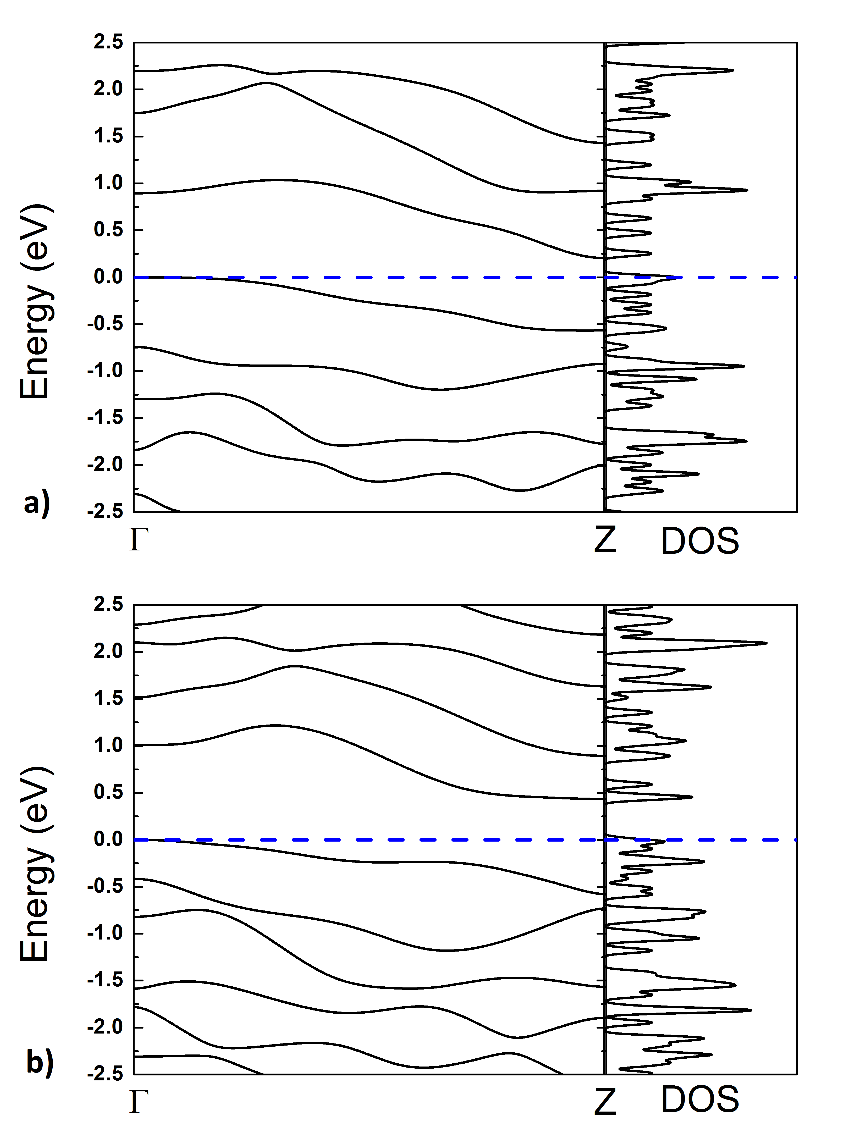
In Figure 4 we present the band structures and the density of states (DOS) for both silicon and germanium tubes. All structures present bands with significant dispersion and small indirect band gaps. The bandgap values are of 0.44 eV and 0.22 eV for silicon and germanium structures, respectively. Even considering the fact that DFT calculations usually underestimate bandgap values Perdew and Levy (1983), these values are reasonably small.
| Bandgap (eV) | (Å) | Young Modulus (TPa) | Poisson Ratio | (eV) | |
|---|---|---|---|---|---|
| Si Tube | 0.22 | 3.777 | 0.25 | 0.12 - 0.12 | -4.02 |
| Si Bulk | - | - | 0.08 | - | -4.93 |
| SiNR | - | - | - | - | -3.84 |
| Ge Tube | 0.44 | 4.026 | 0.15 | 0.07 - 0.06 | -3.52 |
| Ge Bulk | - | - | 0.06 | - | -4.14 |
| GeNR | - | - | - | - | -3.29 |
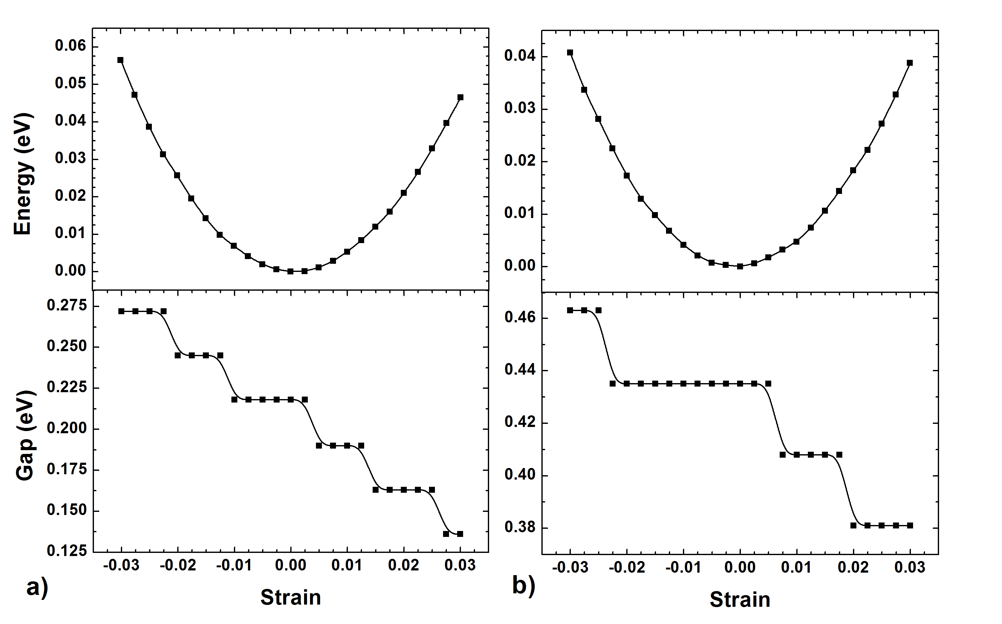
In order to investigate the mechanical properties of these tubes we studied their response to both tensile and compressive strains along their main axis direction. The energy versus strain curves are presented in Figure 5. We restrict ourselves to small strain values in order to maintain the system in the elastic region. In this regime, from the curves in Figure 5 we can estimate the Young’s modulus values for both structures by using
| (1) |
where Y is the Young’s modulus, is the equilibrium volume, U is the total strain energy and is the strain. Using this equation we obtain values of and for the silicon and germanium tubes respectively. These values are quite high and comparable to the values found in strong metal alloys, although not as high as that of graphene, indicating these novel structures present promising mechanical properties. We have also calculated the Poisson’s ratios along the directions shown in Figure 1. This ratio is defined by:
| (2) |
where is the Poisson ratio along the i direction, is the strain along the i direction and is the strain along the axial direction (assuming axial strain is applied). We obtained values of equal to 0.12 and 0.07 and equal to 0.12 and 0.06 for the silicon and germanium structures, respectively.
The electronic and mechanical properties are summarized in Table 1 along with the formation energy, which is defined as the energy per atom necessary for assembling the structure from isolate atoms. The formation energy values shown in Table 1 indicate that the tubular structures are more stable than their corresponding nanoribbons, which is in good accordance with the fact that silicon and germanium nanostructures favor hybridizations over ones. The nanoribbon structures had their geometry optmized following the exact same procedure applied to the tubular structures and presented structural buckling Cahangirov et al. (2009). In order to have a conclusive proof of the stability of the tubular structures, the eigenvalues of the Hessian matrix were calculated. Considering that no negative values were found, we can affirm that they represent a local minimum Banerjee et al. (1985), thus characterizing stable geometries Baker (1986).
Concomitantly with the total energy analysis as a function of strain, we have also analysed the gap variation. The results are presented in Figure 5. The plateaus in the depicted curve are a consequence of the precision of our bandgap calculations of (which is approximately ). As we can see from this figure, there are significant changes on the gap values for both structures as axial strain is applied. Both tubes undergo significant gap opening under compressive strain (negative values of horizontal axis) and gap closing under tensile strain (positive values of horizontal axis). Large gap changes of almost occur under strain rates as small as . These changes at the gap values suggest possible applications of these novel structures as strain sensors and/or other applications where easy tuning of the gap is required.
IV Summary and Conclusions
In summary, we report the theoretical discovery of new silicon and germanium nanotubes which do not have carbon analogues due to the manifestation of the pseudo Jahn-Teller effect. These new structures do not present any helicity despite being neither armchair or zigzag. The tubes exhibit remarkable thermal and electronic properties. Silicon tubes are stable at temperatures as high as 500 K, while germanium ones can reach temperatures as high as 1000 K. Young’s modulus values are considerably high at and and they have small indirect band gap values of and , respectively. These band gap values can be significantly altered, for both structures, by compressive and tensile axial strains. Gap variations almost as large as for strain rates as small as were observed. Such properties could be extremely useful in the design of sensors and other technological devices. We believe these results can motivate new studies of silicon and germanium nanostructures, leading to searches beyond the limited spectrum of existing carbon nanostrucutres and, possibly, to the discovery of new unique and exciting materials.
V ACKNOWLEDGMENTS
The authors thank Dr. Felix Hanke and Prof. J. A. Brum for helpful discussions. We would especially like to thank Prof. D. M. Ugarte for his assistance with the TEM image calculations and very helpful discussions. Work supported in part the the Brazilian Agencies CAPES, CNPq and FAPESP. The authors acknowledge the Center for Computational Engineering and Sciences at Unicamp for financial support through the FAPESP/CEPID Grant #2013/08293-7. RP acknowledges financial support of Fapesp Grant #2011/17253-3.
References
- Kroto et al. (1985) H. W. Kroto, J. R. Heath, S. C. O’Brien, R. F. Curl and R. E. Smalley, Nature, 1985, 318, 162–163.
- Iijima (1991) S. Iijima, nature, 1991, 354, 56–58.
- Novoselov et al. (2004) K. S. Novoselov, A. K. Geim, S. Morozov, D. Jiang, Y. Zhang, S. Dubonos, I. Grigorieva and A. Firsov, Science, 2004, 306, 666–669.
- Röthlisberger et al. (1994) U. Röthlisberger, W. Andreoni and M. Parrinello, Physical review letters, 1994, 72, 665.
- Takeda and Shiraishi (1994) K. Takeda and K. Shiraishi, Physical Review B, 1994, 50, 84246–14922.
- Zunger and Wang (1996) A. Zunger and L.-W. Wang, Applied surface science, 1996, 102, 350–359.
- Singh et al. (2004) A. K. Singh, V. Kumar and Y. Kawazoe, Journal of Materials Chemistry, 2004, 14, 555–563.
- Fagan et al. (2000) S. B. Fagan, R. Baierle, R. Mota, A. J. da Silva and A. Fazzio, Physical Review B, 2000, 61, 9994.
- Guo et al. (2012) L. Guo, X. Zheng, C. Liu, W. Zhou and Z. Zeng, Computational and Theoretical Chemistry, 2012, 982, 17–24.
- Bai et al. (2004) J. Bai, X. Zeng, H. Tanaka and J. Zeng, Proceedings of the National Academy of Sciences of the United States of America, 2004, 101, 2664–2668.
- Sha et al. (2002) J. Sha, J. Niu, X. Ma, J. Xu, X. Zhang, Q. Yang and D. Yang, Advanced Materials, 2002, 14, 1219–1221.
- Zhang et al. (2002) R. Zhang, S. Lee, C.-K. Law, W.-K. Li and B. K. Teo, Chemical physics letters, 2002, 364, 251–258.
- Durgun et al. (2005) E. Durgun, S. Tongay and S. Ciraci, Physical Review B, 2005, 72, 075420.
- Pradhan and Ray (2006) P. Pradhan and A. K. Ray, Journal of Computational and Theoretical Nanoscience, 2006, 3, 128–133.
- Takeda and Shiraishi (1994) K. Takeda and K. Shiraishi, Phys. Rev. B, 1994, 50, 14916–14922.
- Cahangirov et al. (2009) S. Cahangirov, M. Topsakal, E. Aktürk, H. Şahin and S. Ciraci, Physical review letters, 2009, 102, 236804.
- Topsakal and Ciraci (2010) M. Topsakal and S. Ciraci, Physical Review B, 2010, 81, 024107.
- Zhao (2012) H. Zhao, Physics Letters A, 2012, 376, 3546–3550.
- Botari et al. (2014) T. Botari, E. Perim, P. A. S. Autreto, A. C. T. van Duin, R. Paupitz and D. S. Galvao, Phys. Chem. Chem. Phys., 2014, 16, 19417–19423.
- Ni et al. (2011) Z. Ni, Q. Liu, K. Tang, J. Zheng, J. Zhou, R. Qin, Z. Gao, D. Yu and J. Lu, Nano letters, 2011, 12, 113–118.
- O’hare et al. (2012) A. O’hare, F. Kusmartsev and K. Kugel, Nano letters, 2012, 12, 1045–1052.
- Vogt et al. (2012) P. Vogt, P. De Padova, C. Quaresima, J. Avila, E. Frantzeskakis, M. C. Asensio, A. Resta, B. Ealet and G. Le Lay, Physical Review Letters, 2012, 108, 155501.
- Dávila et al. (2014) M. Dávila, L. Xian, S. Cahangirov, A. Rubio and G. Le Lay, New Journal of Physics, 2014, 16, 095002.
- Vogt et al. (2014) P. Vogt, P. Capiod, M. Berthe, A. Resta, P. De Padova, T. Bruhn, G. Le Lay and B. Grandidier, Applied Physics Letters, 2014, 104, 021602.
- Padova et al. (2014) P. D. Padova, C. Ottaviani, C. Quaresima, B. Olivieri, P. Imperatori, E. Salomon, T. Angot, L. Quagliano, C. Romano, A. Vona, M. Muniz-Miranda, A. Generosi, B. Paci and G. L. Lay, 2D Materials, 2014, 1, 021003.
- Hobey (1965) W. D. Hobey, The Journal of Chemical Physics, 1965, 43, 2187.
- Jose and Datta (2012) D. Jose and A. Datta, The Journal of Physical Chemistry C, 2012, 116, 24639–24648.
- Bersuker (2013) I. B. Bersuker, Chemical Reviews, 2013, 113, 1351–1390.
- Delley (2000) B. Delley, Computational materials science, 2000, 17, 122–126.
- Perdew et al. (1996) J. P. Perdew, K. Burke and M. Ernzerhof, Physical review letters, 1996, 77, 3865.
- Koch (2002) C. T. Koch, Determination of core structure periodicity and point defect density along dislocations, 2002.
- Ohnishi et al. (1998) H. Ohnishi, Y. Kondo and K. Takayanagi, Nature, 1998, 395, 780–783.
- Lu et al. (2010) Y. Lu, J. Y. Huang, C. Wang, S. Sun and J. Lou, Nature nanotechnology, 2010, 5, 218–224.
- Troiani et al. (2003) H. Troiani, M. Miki-Yoshida, G. Camacho-Bragado, M. Marques, A. Rubio, J. Ascencio and M. Jose-Yacaman, Nano letters, 2003, 3, 751–755.
- Ajayan and Iijima (1992) P. Ajayan and S. Iijima, Philosophical magazine letters, 1992, 65, 43–48.
- Perdew and Levy (1983) J. P. Perdew and M. Levy, Physical Review Letters, 1983, 51, 1884.
- Banerjee et al. (1985) A. Banerjee, N. Adams, J. Simons and R. Shepard, The Journal of Physical Chemistry, 1985, 89, 52–57.
- Baker (1986) J. Baker, Journal of Computational Chemistry, 1986, 7, 385–395.