Corresponding author: B. Wohlfeil
URL: http://www.tu-berlin.de
URL: http://www.zib.de
URL: http://www.jcmwave.com
URL: http://www.ihp-microelectronics.com
Numerical Simulation of Grating Couplers
for Mode Multiplexed Systems
Abstract
A numerical investigation of a two dimensional integrated fiber grating coupler capable of exciting several LP fiber modes in both TE and TM polarization is presented. Simulation results and an assessment of the numerical complexity of the 3D, fully vectorial finite element model of the device are shown.
keywords:
3D rigorous electromagnetic field simulation, finite-element method,This paper will be published in Proc. SPIE Vol. 8988
(2014) 89880K, (Integrated Optics: Devices, Materials, and Technologies XVIII, DOI: 10.1117/12.2044461),
and is made available
as an electronic preprint with permission of SPIE, ![]() Society of Photo-Optical
Instrumentation Engineers (2014).
One print or electronic copy may be made for personal use only.
Systematic reproduction and distribution, duplication of any
material in this paper for a fee or for commercial purposes,
or modification of the content of the paper are prohibited.
Society of Photo-Optical
Instrumentation Engineers (2014).
One print or electronic copy may be made for personal use only.
Systematic reproduction and distribution, duplication of any
material in this paper for a fee or for commercial purposes,
or modification of the content of the paper are prohibited.
1 Introduction
To avoid the approaching capacity crunch in single mode fiber based transmission systems, which are slowly coming to their theoretical limits, much research has been focused recently on the exploitation of spatial division multiplexing (SDM), especially in the form of multimode transmission. However, to compete with current technologies, the additional modes have to be generated and received in an efficient and cost effective way. Current solutions either lack efficiency [1] or are too complex for a cost effective implementation [2]. Integration on the other hand has proven itself in the past to be a big improvement in these areas. Therefore several solutions based on photonic integrated circuits have been presented [3, 4], albeit still with room for optimization. The device presented in this paper aims to improve upon other solutions by using a single standard sized two dimensional fiber grating coupler, which couples the commonly used fiber modes LP01, LP11a, LP11b and LP21a in TE and TM polarization from photonic nanowires on silicon on insulator to a standard few mode fiber with a high modal overlap and low losses. Simulation results for the performance of the device as well as an estimation of the numerical effort for optimization are presented.
The paper is structured as follows: First the concept for the device itself is presented, followed by an overview over the numerical effort required for the modelling of the device in a three dimensional, fully vectorial finite element solver. Simulation results for the theoretical performance of the coupler are shown and finally the results are summarized with an outlook to future work.
2 Concept
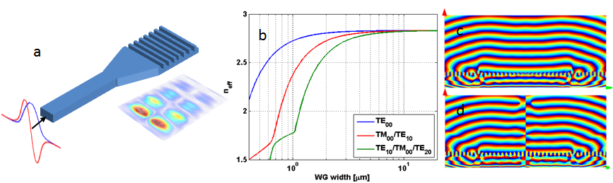
For the excitation of fiber modes the intensity and phase profile of the scattered field of the grating coupler have to be matched to the fiber mode. A standard fiber grating coupler only couples to the LP01 mode, since it only requires a single intensity maximum with a flat phase. For higher order modes, however, several intensity maxima with a relative phase shift between them have to be generated. In the case of the first higher order fiber mode (LP11a), the TE10 integrated waveguide mode can be used to provide the necessary field distribution since it already comes with two intensity maxima with a relative phase shift of 180∘ between them. According to the Bragg condition a grating coupler capable of scattering such a mode can be designed if the period is chosen in accordance with the phase constant of the TE10 mode in the integrated waveguide.
In Figure 1a the scattered vector field above such a grating is shown. As can be seen, the grating excites two very distinct intensity maxima along the transversal direction of the waveguide as it is prescribed by the TE10 waveguide mode. In the lateral direction the grating shows an identical behavior to a standard fiber grating coupler for the fundamental waveguide mode.
For large waveguide widths of around 10 m and larger, which is the usual dimension for fiber grating couplers, the effective indices of the first few guided modes in nanowires are approximately equal (c.f. Figure 1b), resulting in - according to the Bragg relation - equal scattering characteristics, when diffracted by a grating with fixed grating period . Indeed, simple scattering simulations show equal diffraction angle and fraction of out-coupled power for one grating fed with TE00 and TE10 mode, respectively. Therefore, analogously to the excitation of the fundamental fiber mode LP01 through the fundamental waveguide mode TE00 the first higher order waveguide mode TE10 can be used to excite a LP11 fiber mode with a single grating coupler. For the generation of the other LP11 fiber mode the grating is fed from both ends with the fundamental waveguide mode TE00 with a relative phase difference of 180∘ between them. By doing this two distinct intensity maxima along the lateral waveguide direction are excited, as it is necessary for the LP11b fiber mode. If on the other hand the phase shift between the incoming TE00 modes is 0∘ the fields scattered from the opposing ends of the grating do not feature the necessary phase difference to maintain two distinct intensity maxima, resulting in a degeneration to a single intensity maximum. This effect can again be utilized to excite the fundamental fiber mode LP01. Figures 1 c and d show the phase profiles of the electric fields in a cross-sectional view of a grating coupler that is excited from both ends (left and right) with the fundamental waveguide mode with a 0∘ (c) and a 180∘ (d) phase difference, respectively.
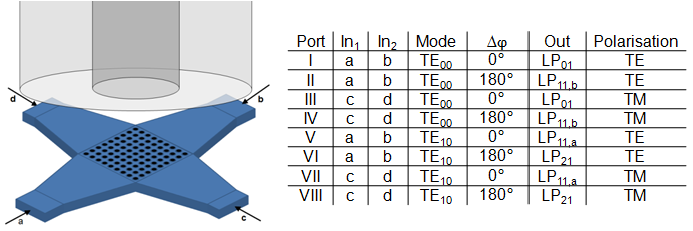
Since the grating shows equal scattering properties for TE00 and TE10 modes the same is true for an incoming TE10 from both ends of the grating: If the phase difference is 0∘ the fields from both ends will melt together, producing the LP11a fiber mode. With a phase difference of 180∘ the incoming TE10 modes from both ends are detached from each other creating four distinct intensity maxima as exhibited by the LP21 fiber mode. The complete layout of the grating together with a table of all excitable fiber modes can be seen in Figure 2. Note that a two dimensional grating is used for the operation in both TE and TM polarization. To excite fiber modes in TE polarization input waveguides a and b are used, while for TM polarized modes waveguides c and d need to be excited. Each waveguide pair is fed with TE00 or TE10 modes with either 0∘ or 180∘ phase difference resulting in four different fiber modes per polarization. Due to the forced symmetry by the way of excitation the coupled fiber needs to be strictly vertical in contrast to conventional fiber-grating coupling. Therefore, more care has to be taken, when considering reflections between fiber facet and grating.
Since the orthogonality of the fiber modes is maintained at every part of the device all modes can be excited independently of each other at the same time.
3 Numerical method
For optimizing the design parameters of a fiber grating coupler we perform numerical simulations of light propagation through the device. The relevant physical model in this case are Maxwell’s equations, with the full 3D geometrical structure of the device. As we are interested in the wavelength-dependence of the coupling efficiency of specific field patterns we perform time-harmonic (steady-state) light scattering simulations of incoming waveguide modes for the wavelength range of interest. For this we use the Maxwell solver JCMsuite [5] based on the finite-element method (FEM) [6].
Due to the relatively large size of the 3D computational domain and possible resonance / interference effects, it can be challenging to obtain field solutions which are accurate enough for reliable optimization [7]. However, using finite-elements of higher polynomial order allows to obtain sufficiently accurate results within resonable computation times. The simulation flow is as follows: A wavelength scan is performed for the wavelength range of interest. For each wavelength :
-
•
the waveguide modes of the waveguides entering the computational domain from the side are computed,
-
•
a specific mode is defined as source field for a light scattering problem for the full 3D computational domain containing the grating coupler and the incoming waveguides (see, e.g., Fig. 2 left),
-
•
the full 3D near field field distribution is computed as solution to above scattering problem,
-
•
the electromagnetic near field distribution is exported in a plane parallel to the grating coupler surface, located m above the grating surface,
-
•
overlap integrals between above scattered light field and the light fields corresponding to fundamental and higher order fiber modes are computed.
For computation of the waveguide modes we solve an eigenvalue problem on a 2D computational domain containing the waveguide structure. By using higher order finite-elements and adaptive mesh refinement, very high accuracies can easily be reached, such that the influence of numerical discretization errors in this step can be neglected [8]. Typically we choose the following numerical parameters: polynomial degree of the finite-element ansatz functions and several adaptive mesh refinement steps resulting in an unstructured spatial mesh with triangle sidelengths of sizes between roughly nm and few nm. For the 3D computations, a prismatoidal mesh is generated by extruding a description of the -cross-section of the device in direction. In each layer of the extrusion, variable domain identifiers are attributed to the extruded 3D objects. This allows for fast and stable construction of the 3D mesh. The mesh is constructed from prism elements, and typical sidelengths of the prisms in -direction depend on sizes of the involved layers, up to microns. Typical sidelengths of the mesh elements in the -plane depend on (and are smaller than) the dimensions of the etched structures of few nm. Automatic, error-controlled mesh refinement in -direction, performed by the FEM solver and depending on chosen parameter yields correspondingly fine meshes also in -direction. For the study presented in this paper we have choosen the numerical parameter polynomial degree of the finite-element ansatz functions as . We have also tested (not shown here) to choose different finite-element degrees in horizontal and vertial direction, and found that performance can be improved by using higher degrees in -direction.
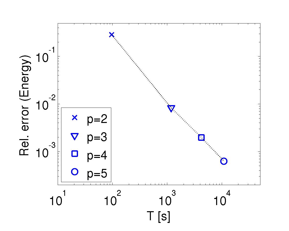
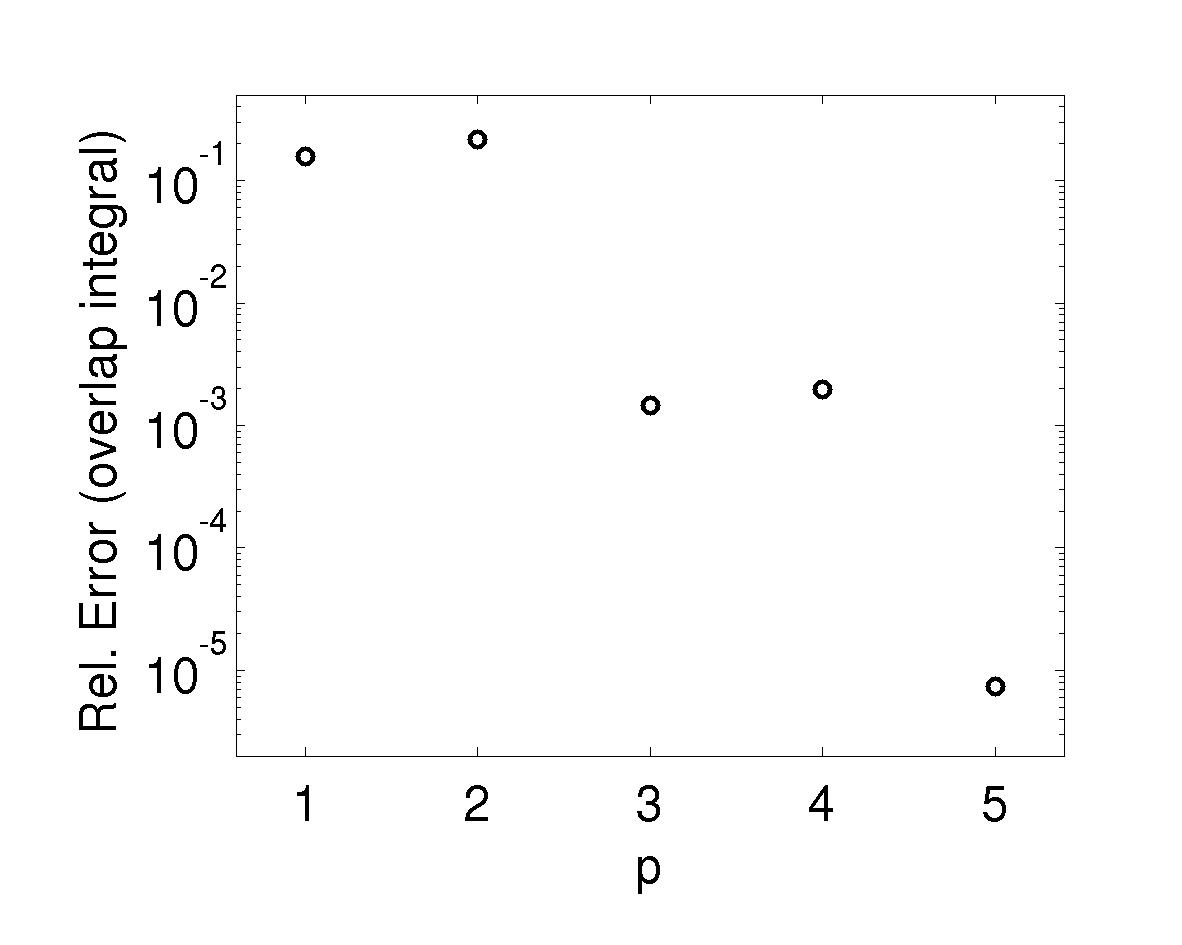
The choice of the numerical parameters is validated in a convergence study: For this aim we have varied finite-element degree and observed quantitative impact on the simulation results. The model problem for the convergence study consists of a 3D grating with square-shaped etched pits () at a periodicity length of nm. In propagation direction () of the incoming waveguide, the grating has 21 pits, while in the transveral direction () infinite periodicity is assumed, such that the size of the computational domain in -direction is with appropriate boundary conditions. The total computational domain, including incoming waveguides, substrate, buffer layer (2 m), grating structure and air superspace is , corresponding to roughly 200 cubic wavelengths at vacuum wavelength of m.
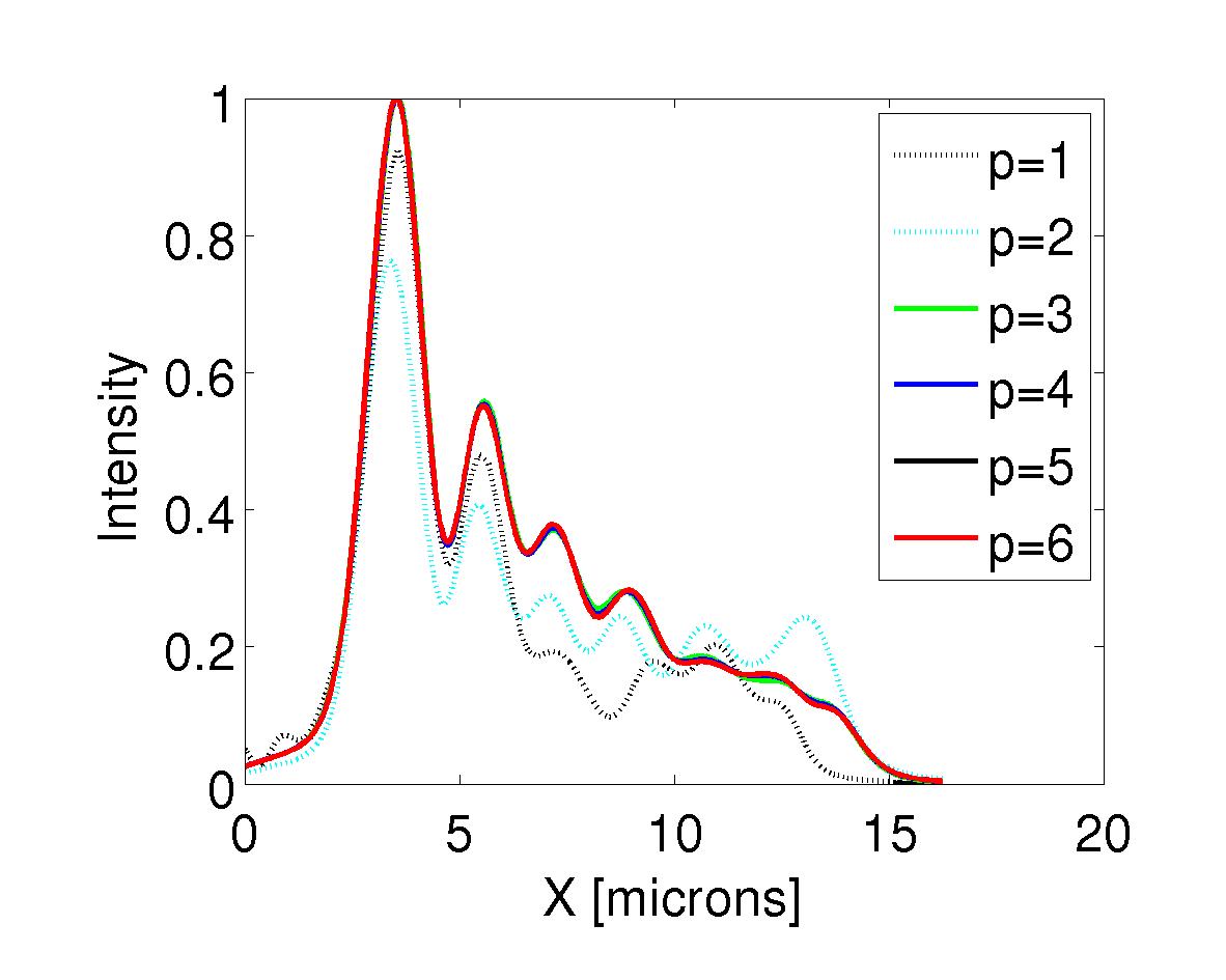
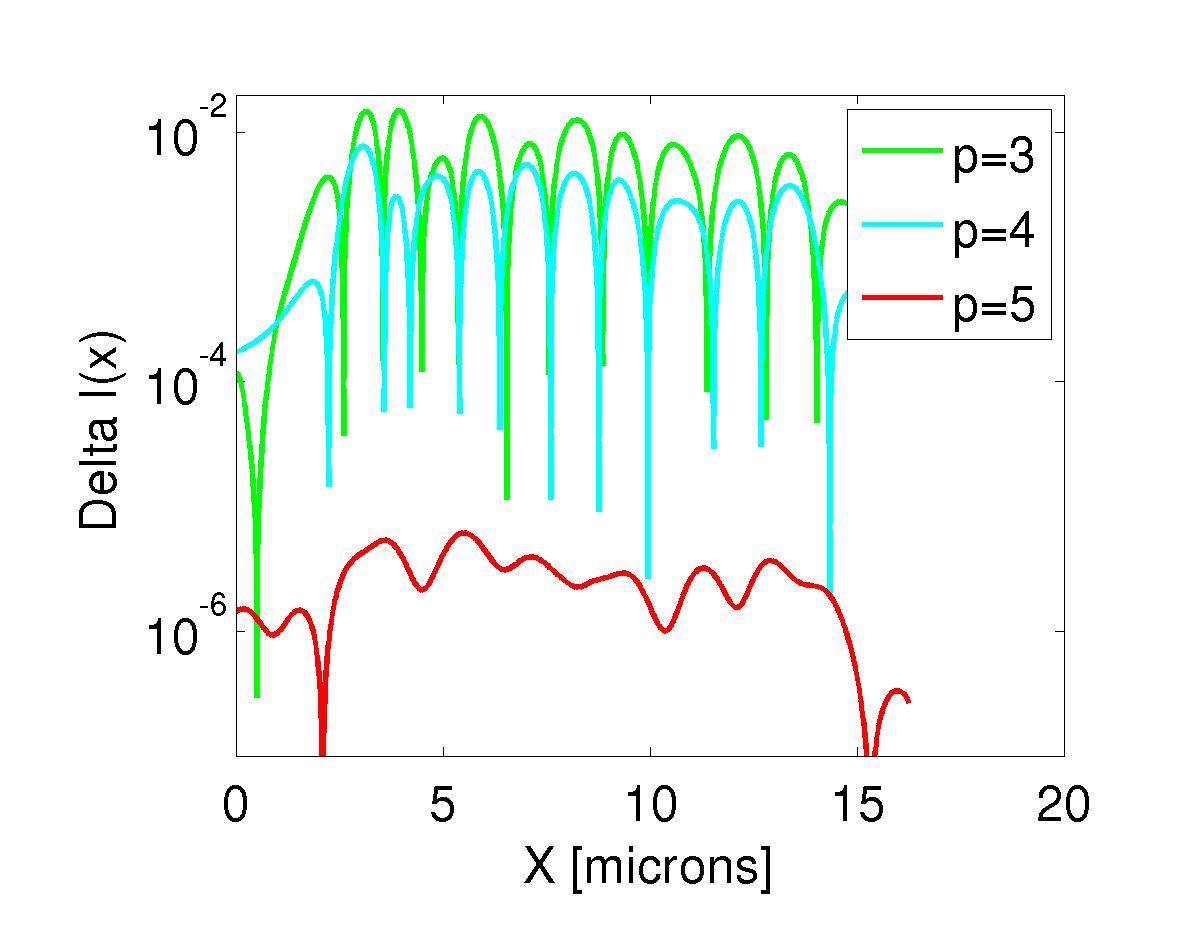
Figure 3 shows convergence of the results with varied finite-element degree : in Fig. 3 a the relative error of the total field energy, , is plotted for various settings of in dependence of total computation time (CPU time on a standard workstation). The total field energy is the integral over the electromagnetic field energy density, integrated over the volume of the computational domain. The relative error is in relation to the value computed from the FEM solution at highest numerical resolution (at , also called quasi-exact solution). Figure 3 b shows convergence of the overlap integral of the intensity distribution exported to a cartesian grid with points with the intensity distribution exported from the quasi-exact solution. This is the quantity of interest for the optimization of the grating geometrical parameters. From the Figure it can be seen that relative numerical errors well below 1% are reached for . This error level is sufficient for performing optimizations where the quantity of interest varies by significantly larger amounts.
Figure 4 a shows the field distributions for the solutions at different numerical resolution in -direction, above the grating, integrated in -direction. As expected from the convergence results above, the field distributions are quite stable for . Figure 4 b shows the deviations of the same distributions from the quasi-exact solution. For pointwise deviations are well below 1%. In summary, the convergence study shows that the numerical error for this problem type is well controllable and that numerical parameter regimes can easily be found which allow for fast and sufficiently accurate performance of the solver in optimization loops. In principle, performance can further be improved by, e.g., using reduced basis methods [9] or / and automatic computation of parameter derivatives [10].
4 Numerical results
In the best case one can achieve a consistently high field overlap between scattered fields and desired fiber modes together with a high directionality (fraction of power scattered towards the fiber) of the grating. For this device an epitaxial silicon overlay of 150 nm on top of the grating was employed to increase the overall coupling efficiency of the grating. The two most important design parameters for this device are the grating length as determined by the number of grating periods and the etch depth of the grating, which mainly defines the grating strength and therefore at which position along the axis of propagation in the grating the intensity maxima are located. Together the parameters need to be chosen so that the distance between fields scattered from opposing ends of the grating is not too big to prevent a melting together of the fields for the generation of the LP01 mode and not too small for the formation of the LP11b fiber mode. The shape of the LP11a mode is mainly determined by the width of the grating coupler, which is equal to its length, due to symmetry (see Figure 2). The grating period is for the most part a function of the wavelength the device is operated at. The duty cycle of the grating (fraction of etched to non-etched area) can be chosen freely, but should not be too small since this would result in a transparent grating. Here a grating etch depth of 210 nm was chosen, since in combination with a silicon overlay of 150 nm on top of the 220 nm waveguide height results in a high directionality (fraction of power scattered upwards) of the grating coupler. Together with 21 grating periods this leads to good field overlaps between scattered fields and fiber modes. As a figure of merit across all fiber modes was introduced, where p is the fraction of power scattered towards the fiber independent of the way of excitation and is the overlap with the excited fiber mode. The overlap with LP21 is missing here since only one of the modes in this group can be excited and therefore the mode group would be incomplete.
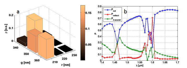
Figure 5a shows the figure of merit as a function of two grating design parameters groove-width g (etched part of the grating period) and ridge-width r (non etched part of the grating period). A grating with a period of around 560 nm gives the best results on average across all three fiber modes. However, for slightly varying grating periods the performance of the device drops rapidly, indicating a low tolerance for the manufacturing process. Nevertheless, with an adaptation of the etch depth a potential deviation of the grating period can be compensated. A filter curve of a two dimensional grating with a period of 560 nm is depicted in Figure 5b, where the blue line indicates the out-coupled power. Due to the silicon overlay and the deep etch depth such a grating can be quite efficient, peaking at a wavelength of 1550 nm. For longer wavelengths the power scattered towards the fiber decreases sharply and transmission (green line) and reflection (red line) increase.
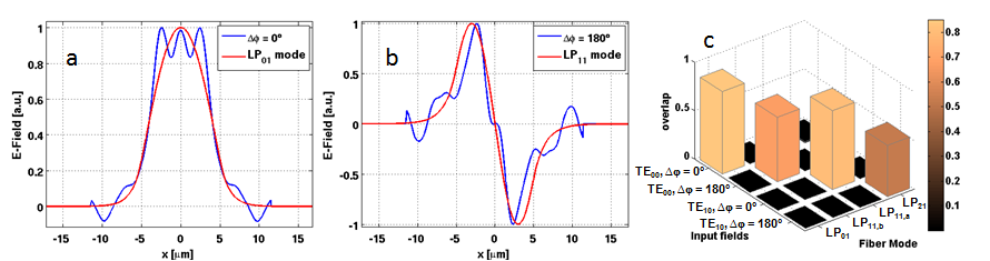
A cross section of the electric fields emitted by the grating can be seen in Figures 6a and b. The overlap with the desired fiber modes (here LP01 and LP11b) is clearly evident, thus – together with the high directionality of the grating – giving a good coupling efficiency. Figure 6c shows the complete overlaps calculated from the fields of fully 3D light scattering simulations with all excitable fiber modes. Being in a not fully excitable mode group the performance of the LP21a mode was neglected for the optimization of the grating, resulting in the lowest field overlap of only 50%. All other modes show a high overlap of 70% and above with the scattered fields, when the grating is excited correspondingly. Higher overlaps of 90% for singular modes can be achieved with adapted grating designs, but the performance of other modes would be affected negatively. Due to the mentioned orthogonality of the fields involved at every stage in the device the extinction of unwanted modes is also very large, with power ratios always below 10-6.
5 Conclusion
We presented a numerical investigation of a two dimensional fiber grating coupler capable of exciting the LP01, LP11a, LP11b and LP21a fiber mode in TE and TM polarization. Accurate solutions for the challenging 3D light scattering problem have been validated in a convergence study. Simulations show a good performance of the grating and high modal overlaps between scattered fields and fiber modes and a very low crosstalk between modes.
Acknowledgments
This work has been partially supported by the European commission through project ICT-GALACTICO, grant agreement 258407, by BMBF within project Mosaic (FKZ 13N12438), and by German Research Foundation DFG through SFB 787.
References
- [1] Salsi, M., Koebele, C., Sperti, D., Tran, P., Brindel, P., Mardoyan, H., Bigo, S., Boutin, A., Verluise, F., Sillard, P., Bigot-Astruc, M., Provost, L., Cerou, F., and Charlet, G., “Transmission at 2x100Gb/s, over two modes of 40km-long prototype few-mode fiber, using LCOS based mode multiplexer and demultiplexer,” in [Optical Fiber Communication Conference/National Fiber Optic Engineers Conference 2011 ], PDPB9, Optical Society of America (2011).
- [2] Klaus, W., Sakaguchi, J., Puttnam, B., Awaji, Y., Wada, N., Kobayashi, T., and Watanabe, M., “Free-space coupling optics for multicore fibers,” Photonics Technology Letters, IEEE 24, 1902–1905 (2012).
- [3] Doerr, C. R., Fontaine, N., Hirano, M., Sasaki, T., Buhl, L., and Winzer, P., “Silicon photonic integrated circuit for coupling to a ring-core multimode fiber for space-division multiplexing,” 37th European Conference and Exposition on Optical Communications , Th.13.A.3, Optical Society of America (2011).
- [4] Fontaine, N. K., Doerr, C. R., Mestre, M. A., Ryf, R., Winzer, P., Buhl, L., Sun, Y., Jiang, X., and Lingle, R., “Space-division multiplexing and all-optical MIMO demultiplexing using a photonic integrated circuit,” Optical Fiber Communication Conference , PDP5B.1, Optical Society of America (2012).
- [5] Burger, S., Zschiedrich, L., Pomplun, J., and Schmidt, F., “JCMsuite: An adaptive FEM solver for precise simulations in nano-optics,” in [Integrated Photonics and Nanophotonics Research and Applications ], ITuE4, Optical Society of America (2008).
- [6] Pomplun, J., Burger, S., Zschiedrich, L., and Schmidt, F., “Adaptive finite element method for simulation of optical nano structures,” phys. stat. sol. (b) 244, 3419 (2007).
- [7] Maes, B., Petráček, J., Burger, S., Kwiecien, P., Luksch, J., and Richter, I., “Simulations of high-Q optical nanocavities with a gradual 1D bandgap,” Opt. Express 21, 6794 (2013).
- [8] Burger, S., Zschiedrich, L., Pomplun, J., and Schmidt, F., “Finite element method for accurate 3D simulation of plasmonic waveguides,” Proc. SPIE 7604, 76040F (2010).
- [9] Pomplun, J. and Schmidt, F., “Accelerated a posteriori error estimation for the reduced basis method with application to 3D electromagnetic scattering problems,” SIAM J. Sci. Comput. 32, 498–520 (2010).
- [10] Burger, S., Zschiedrich, L., Pomplun, J., Schmidt, F., and Bodermann, B., “Fast simulation method for parameter reconstruction in optical metrology,” Proc. SPIE 8681, 868119 (2013).