Investigation of the Mn3-δGa/MgO interface for magnetic tunneling junctions
Abstract
The Mn3Ga Heusler compound and related alloys are the most promising materials for the realization of spin-transfer-torque switching in magneto tunneling junctions. Improved performance can be achieved by high quality interfaces in these multilayered structured devices. In this context, the interface between Mn1.63Ga and MgO is of particular interest because of its spin polarization properties in tunneling junctions. We performed a chemical characterization of the MgO/Mn1.63Ga junction by hard x-ray photoelectron spectroscopy. The experiment indicated the formation of Ga-O bonds at the interface and evidenced changes in the local environment of Mn atoms in the proximity of the MgO film. In addition, we show that the insertion of a metallic Mg-layer interfacing the MgO and Mn–Ga film strongly suppresses the oxidation of gallium.
pacs:
79.60.Jv, 79.60.Dp, 75.30.Gw, 75.70.AkThe engineering of a high performance magnetic tunneling junction (MTJ) is crucial for the emergence of a new class of non-volatile memories and spintronic devices. Directly related with these recent technologies, Mn2YZ Heusler compounds, where Y is a transition metal and Z is a main group element, have shown interesting properties such as high spin polarization, high Curie temperature (Tc), low net magnetic moment, and strong magneto-crystalline anisotropyGraf, Felser, and Parkin (2011). Mn3Ga and related alloys appear as promising materials in the realization of switching type spin-transfer-torque mangnetoresistive random access memories (STT-MRAMs). Mn–Ga films present perpendicular magneto anisotropy (PMA) and a nearly compensated ferrimagnetic phaseDjayaprawira et al. (2005); Ikeda et al. (2010); Kubota et al. (2011a); Mizukami et al. (2012); Bai et al. (2012). These characteristics are important for the reduction of the switching current and downscaling of the dimensions while maintaining thermal stability in STT-MRAM devicesBalke et al. (2007). The full understanding and control of growth properties of the Mn–Ga/MgO system will open up avenues for the exploitation of Heusler compounds in ultra-high density memory technologies.
The performance of MTJ devices is strongly influenced by the quality of the film interfaces. Long-range ordering of the two-dimensional interfaces is required for conservation of the electron moment transverse to the tunneling current propagation ().Zhang and Butler (2004) The integration of Heusler compounds in MTJs has been successfully demonstrated for Co2MnSiKrumme et al. (2012); Tsunegi et al. (2008). The great advantage of the Mn2YZ family over other Heuslers is the tetragonal distortion of the crystalline structure leading to the PMA. This allows an unique combination of high-spin polarization with perpendicular magnetization in MTJs. Recent studies on the engineering of MTJs using Mn–Ga alloys by Kubota et al. Kubota et al. (2011b, c, a) resulted in the optimized layered structure: Cr buffer/Mn–Ga/MgO/CoFe. The MgO grows compressed on the Mn–Ga structure with a lattice mismatch of approximately 7%Kubota et al. (2011a), which can cause lattice dislocations reducing the crystalline ordering. An insertion of a 4 Å metallic Mg layer interfacing MgO and Mn–Ga promotes a slight increase of the tunneling magnetoresistance ratio, which reached 23% in Mn1.63GaKubota et al. (2011a). The insertion is believed to improve the crystalline quality of MgO film and acts to diminish the oxidation of the Mn and Ga atoms at the interface.Kubota et al. (2011a) The knowledge of the actual chemical composition at the interface is essential for taking full advantage of the special spin properties of the Mn–Ga films and reaching higher TMR ratios.
In the present work, the MgO(001)/Mn1.63Ga(001) junction was investigated by hard x-ray photoelectron spectroscopy (HAXPES). We found the presence of a gallium oxide layer at the interface and show that the insertion of the metallic Mg layer strongly suppresses the formation of this oxide. HAXPES can efficiently probe burier layers Kozina et al. (2011) and interfacesPaul et al. (2009) because of the large escape depth of high kinetic energy photoelectrons. The experiments using a photon energy of h = 3.0 keV, with a total resolution of 400 meV, were carried out in the P09 beamline of DESY (Germany); and those using h = 7.9 keV, with a total resolution of 250 meV, were carried out in the BL47-XU beamline of SPring-8 (Japan)Ikenaga et al. (2013). Fig. 1(a) depicts the experimental geometry in both setups. The angle between the electron spectrometer and photon propagation is fixed at and the photoemitted electrons were collected at angle . Samples were measured at RT ( 300 K). We investigated the following structures: Cr buffer(40)/Mn1.63Ga(30)/Mg()/MgO(2)/AlO(1) with = 0 (sample 1) and 0.4 (sample 2), where the numbers in parentheses indicate the thickness in nm. Films were grown using an ultrahigh-vacuum magnetron sputtering system on MgO(001) substrate and capped with 1 nm Al layer. Growth details can be found in the Ref. Kubota et al., 2011b.
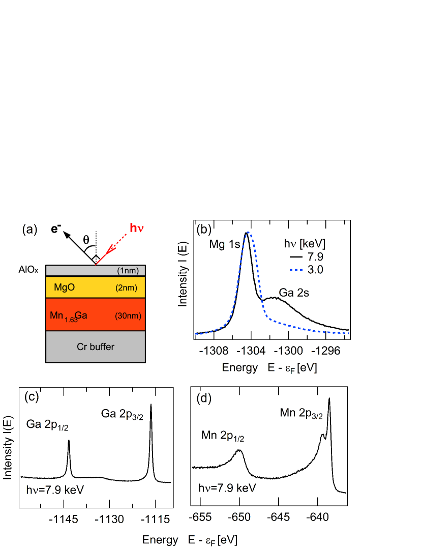
To understand the chemical composition near to the MgO/Mn1.63Ga interface, we compared the photoemission spectral shapes measured by different photon energies. Fig. 1(b) shows the spectra of the Mg 1s and Ga 2s measured by a photon energy of 7.9 (solid line) and 3.0 keV (dashed line). The Ga 2s peak from the buried Mn1.63Ga film is clearly visible in the 7.9 keV spectra, while it is only distinguishable as a shape asymmetry of the Mg 1s peak in the 3.0 keV spectra. This is because the photon energy of 7.9 keV produces photoelectrons with a large escape depth and, consequently, positions much deeper than the interface were probed. In contrast, the probed depth using a photon energy of 3.0 keV extends only up to near the MgO/Mn1.63Ga interface. For Ga 2s photoelectrons, the mean free path through MgO and the capping layer is about 10 (3.3) nm for a photon excitation of 7.9 (3.0) keV, according to the TPP-2M formulaTanuma, Powell, and Penn (1994).
By using 7.9 keV, we measured the Ga and Mn 2p core states as shown in Figs. 1(c) and (d), respectively. The presence of Ga oxides are commonly identified by a shoulder at high binding energy tail of the main Ga 2p3/2 peak, as will be discussed later. In Fig. 1(c), a direct inspection in the Ga 2p3/2 peak, located at 1143.4 eV, excludes any substantial amount of oxides in the bulk part of the film. In Fig. 1(d), the Mn 2p1/2 state was assigned to a broad peak at about 650.0 eV, while Mn 2p3/2 exhibited a sharp double-peak structure around 638.8 eV. The higher binding energy peak of the 2p3/2 level originated from poorly screened states, while the lower binding energy peak was associated with well-screened final statesFujii et al. (2011). The relative high intensity of the well-screened peak is not usually observed in the presence of Mn oxides, which exhibits a Mn 2p3/2 peak located at energies above 640 eVNelson, Reynolds, and Roos (2000); Hishida, Ohbayashi, and Saitoh (2013). The Ga and Mn 2p spectra shown in Figs 1(c) and (d) can therefore be safely assumed as references of the spectral shape expected for a homogeneous Mn1.63Ga film.
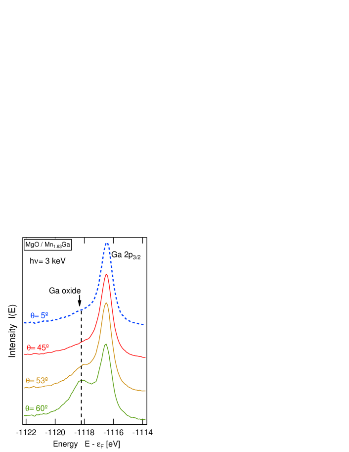
Information about the depth profile of the interface was obtained by comparing near-normal () and off-normal () photoemission spectra using 3 keV photon energy. Electrons emitted at off-normal directions travel longer distances inside the material, for this reason they are more subjected to scattering, resulting in an escape depth of approximately 3cos(). Fig. 2 shows the Ga 2p3/2 spectra for the sample 1 measured from to . Spectra measured at (dashed line) presented a small shoulder at higher binding energies consistent with the presence of Ga oxides near the interface. The shoulder was due to the overlap of the main peak with the oxide peak, which chemically shifted to higher binding energies, as reported for oxidized GaAs filmsMassies and Contour (1985); Paul et al. (2009). As increases, the probe depth is reduced and the contribution of the interface is enhanced. At , the shoulder slightly increased. From the shoulder strongly increased until it became a distinguishable peak at , which was located 1.7 eV below the main peak. The sudden onset of the Ga oxide peak between and can be explained by a sharp concentration of the oxide at the interface, which contributes to the photoemission spectra at high photoemission angles (short electron escape depth).
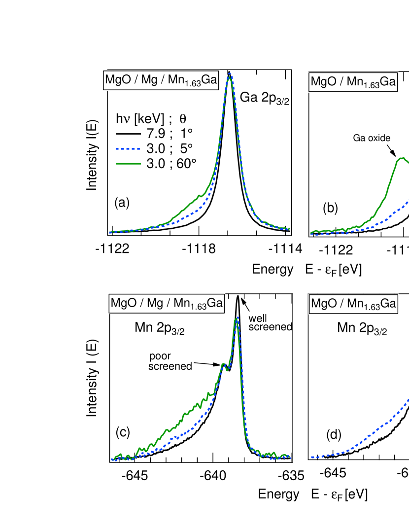
In Fig. 3, we show the influence of the insertion of the Mg metallic layer by comparison of the spectra obtained for the sample 2; (a) and (c); and sample 1; (b) and (d). Figs. 3(a) and (b) show the Ga 2p3/2 spectra measured in different configurations. For both samples, it was observed an increase of the high binding energy shoulder from 7.9 to 3.0 keV photon energy in near-normal photoemission. However, in contrast with sample 1, sample 2 does not exhibit a distinguishable oxide peak at high photoemission angles (). The absence of a clear oxide peak in the Fig. 3(a) implies that the insertion of metallic Mg layer suppressed the formation of Ga oxide at the interface.
Fig. 3(c) shows the Mn 2p3/2 spectra for sample 2. From 7.9 to 3.0 keV, we observed a broadening of the spectra towards high binding energies. We also noticed a reduction of the well-screened peak with respect to the poorly screened peak. Interestingly, the broadening increased at , which means that this feature is enhanced in the proximity of the MgO/Mn1.63Ga interface. The relative intensity of the double peaks was unaltered by changing the photoemission angle. In Fig. 3(d), the Mn 2p3/2 spectra measured with 7.9 keV photon energy for sample 1 [shown also in Fig. 1(d)] is compared with the measurement using 3.0 keV photon energy. The same trends observed for sample 2 were also present here.
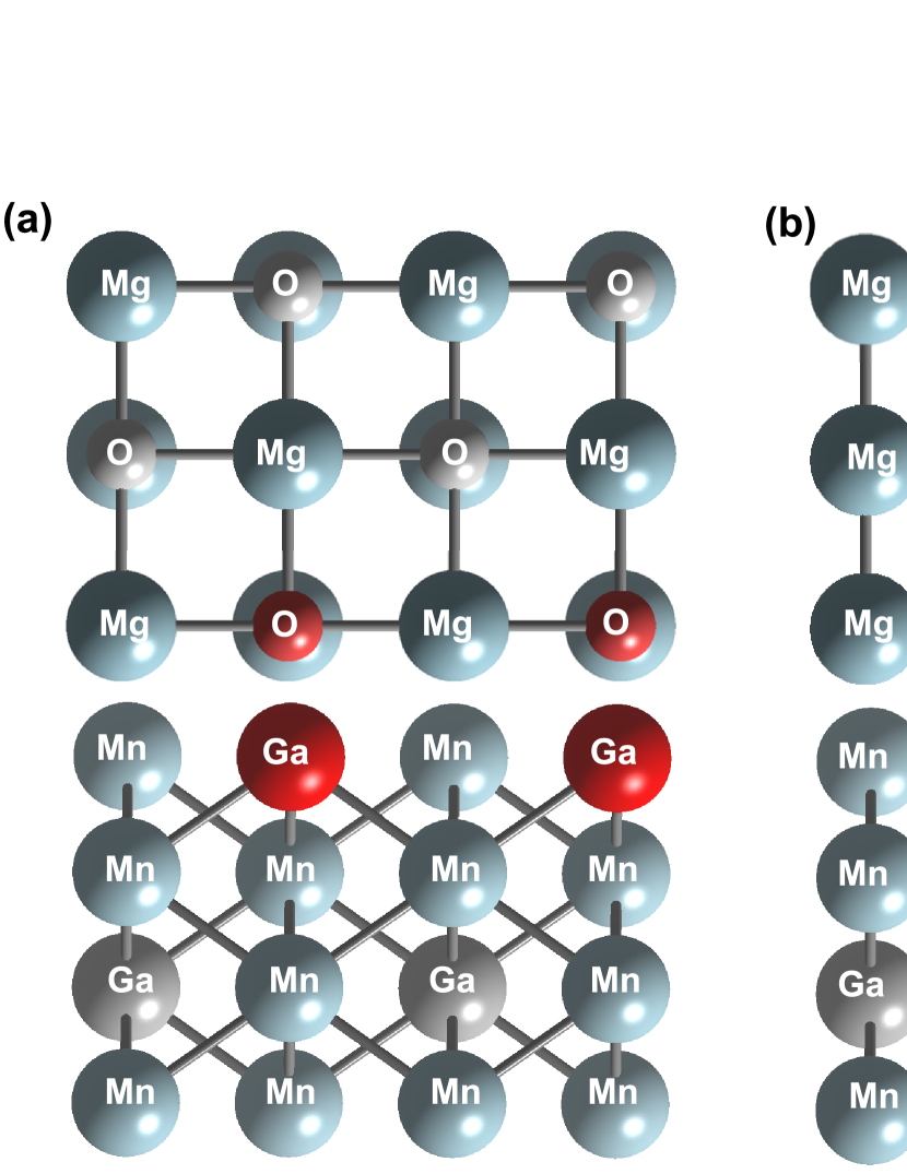
The comparison between spectra measured at different photoemission angles was not conclusive in respect to the presence of Mn oxides. Clearly, the local environment of Mn atoms changes from deep positions inside the film to that near the MgO interface independently on the presence of the Mg layer. The reduction of the well-screened peak intensity and broadening of the Mn 2p3/2 spectra, when measured by the 3 keV photon energy, indicate a weakening of the hybridization of Mn valence states near the interface. Concerning the Ga oxides, their high concentration at the interface of sample 1 can be explained by the hypotheses of a Ga-rich interface. The Mn3Ga structure is composed of periodically stacked Mn–Mn and Ga–Mn atomic layers. The interface with the Ga–Mn termination plane is thermodynamically the most stable according to recent ab-initio calculationsMiura and Shirai (2014), as illustrated in Fig. 4(a). Therefore, Mn1.63Ga might present a Ga–Mn termination plane, which is formed mostly by Ga atoms due to the low Mn content. This would prompt the formation of Ga oxides at the interface. The oxidation of Ga is strongly reduced by using the metallic Mg spacer layer as depicted in Fig. 4(b).
At this point, the investigation of other Mn2YZ systems providing better interface properties with MgO would be an interesting option. The Mn3Ge is one feasible candidateMizukami et al. (2013), since ab-initio calculations predicted high TMR ratios independently on the interface terminationMiura and Shirai (2014). Alternatively, the engineering of compounds using main group elements Z with larger atomic radii, as Sb and Sn, would favor better lattice matching with MgO. The optional configuration should also take into account the reactivity of the elements with oxygen. The combination of these properties will be the key for reaching ultra-high TMR ratios in Heusler-base MTJ, consisting in a challenge for both theoreticians and experimentalists.
In summary, we investigated the MgO/Mn1.63Ga junction grown by sputtering deposition and the influence of the insertion of a thin metallic Mg layer at the interface. Depth-resolved chemical information could be obtained by changing the photon energy and photoemission angle in the HAXPES experiment. The local environment of Mn atoms strongly changes near the MgO interface. The experiment points to a reduction of the hybridization for shallow Mn atoms. This behavior seems not to be affected by the insertion of the metallic Mg layer. The angular dependence of photoelectrons provides evidences for the formation of Ga oxide concentrated at MgO/Mn1.63Ga interface. The formation of Ga oxide is suppressed by the insertion of the metallic Mg layer. We ascribe the presence of Ga oxide to a Ga-rich interface due to the low Mn content in the Mn1.63Ga film. This information will stimulate the investigation of new growth methodologies and engineering of MTJs.
Acknowledgments
Financial support by Deutsche Forschungsgemeinschaft and the Strategic International Cooperative Program of JST (DFG-JST) (Project P1.3-A of research unit FOR 1464: ASPIMATT) is gratefully acknowledged. HAXPES experiments were performed at BL47XU of SPring-8 with approval of JASRI (Proposal No. 2012B0043) and at P09 of DESY (Project No. I-20120684).
References
- Graf, Felser, and Parkin (2011) T. Graf, C. Felser, and S. S. Parkin, Progress in Solid State Chemistry 39, 1 (2011).
- Djayaprawira et al. (2005) D. D. Djayaprawira, K. Tsunekawa, M. Nagai, H. Maehara, S. Yamagata, N. Watanabe, S. Yuasa, Y. Suzuki, and K. Ando, Applied Physics Letters 86, 092502 (2005).
- Ikeda et al. (2010) S. Ikeda, K. Miura, H. Yamamoto, K. Mizunuma, H. D. Gan, M. Endo, S. Kanai, J. Hayakawa, F. Matsukura, and H. Ohno, Nat Mater 9, 721 (2010), 10.1038/nmat2804.
- Kubota et al. (2011a) T. Kubota, M. Araidai, S. Mizukami, X. Zhang, Q. Ma, H. Naganuma, M. Oogane, Y. Ando, M. Tsukada, and T. Miyazaki, Applied Physics Letters 99, 192509 (2011a).
- Mizukami et al. (2012) S. Mizukami, T. Kubota, F. Wu, X. Zhang, T. Miyazaki, H. Naganuma, M. Oogane, A. Sakuma, and Y. Ando, Phys. Rev. B 85, 014416 (2012).
- Bai et al. (2012) Z. Bai, Y. Cai, L. Shen, M. Yang, V. Ko, G. Han, and Y. Feng, Applied Physics Letters 100, 022408 (2012).
- Balke et al. (2007) B. Balke, G. H. Fecher, J. Winterlik, and C. Felser, Applied Physics Letters 90, 152504 (2007).
- Zhang and Butler (2004) X.-G. Zhang and W. H. Butler, Phys. Rev. B 70, 172407 (2004).
- Krumme et al. (2012) B. Krumme, D. Ebke, C. Weis, S. I. Makarov, A. Warland, A. Hatten, and H. Wende, Applied Physics Letters 101, 232403 (2012).
- Tsunegi et al. (2008) S. Tsunegi, Y. Sakuraba, M. Oogane, K. Takanashi, and Y. Ando, Applied Physics Letters 93, 112506 (2008).
- Kubota et al. (2011b) T. Kubota, Y. Miura, D. Watanabe, S. Mizukami, F. Wu, H. Naganuma, X. Zhang, M. Oogane, M. Shirai, Y. Ando, and T. Miyazaki, Applied Physics Express 4, 043002 (2011b).
- Kubota et al. (2011c) T. Kubota, S. Mizukami, D. Watanabe, F. Wu, X. Zhang, H. Naganuma, M. Oogane, Y. Ando, and T. Miyazaki, Journal of Applied Physics 110, 013915 (2011c).
- Kozina et al. (2011) X. Kozina, G. H. Fecher, G. Stryganyuk, S. Ouardi, B. Balke, C. Felser, G. Schönhense, E. Ikenaga, T. Sugiyama, N. Kawamura, M. Suzuki, T. Taira, T. Uemura, M. Yamamoto, H. Sukegawa, W. Wang, K. Inomata, and K. Kobayashi, Phys. Rev. B 84, 054449 (2011).
- Paul et al. (2009) M. Paul, A. Müller, A. Ruff, B. Schmid, G. Berner, M. Mertin, M. Sing, and R. Claessen, Phys. Rev. B 79, 233101 (2009).
- Ikenaga et al. (2013) E. Ikenaga, M. Kobata, H. Matsuda, T. Sugiyama, H. Daimon, and K. Kobayashi, Journal of Electron Spectroscopy and Related Phenomena 190, Part B, 180 (2013), recent advances in Hard X-ray Photoelectron Spectroscopy (HAXPES).
- Tanuma, Powell, and Penn (1994) S. Tanuma, C. J. Powell, and D. R. Penn, Surface and Interface Analysis 21, 165 (1994).
- Fujii et al. (2011) J. Fujii, M. Sperl, S. Ueda, K. Kobayashi, Y. Yamashita, M. Kobata, P. Torelli, F. Borgatti, M. Utz, C. S. Fadley, A. X. Gray, G. Monaco, C. H. Back, G. van der Laan, and G. Panaccione, Phys. Rev. Lett. 107, 187203 (2011).
- Nelson, Reynolds, and Roos (2000) A. J. Nelson, J. G. Reynolds, and J. W. Roos, Journal of Vacuum Science and Technology A 18, 1072 (2000).
- Hishida, Ohbayashi, and Saitoh (2013) T. Hishida, K. Ohbayashi, and T. Saitoh, Journal of Applied Physics 113, 043710 (2013).
- Massies and Contour (1985) J. Massies and J. P. Contour, Journal of Applied Physics 58, 806 (1985).
- Miura and Shirai (2014) Y. Miura and M. Shirai, Magnetics, IEEE Transactions on 50, 1 (2014).
- Mizukami et al. (2013) S. Mizukami, A. Sakuma, A. Sugihara, T. Kubota, Y. Kondo, H. Tsuchiura, and T. Miyazaki, Applied Physics Express 6, 123002 (2013).