Electrons and phonons in single layers of hexagonal indium chalcogenides from ab initio calculations
Abstract
We use density functional theory to calculate the electronic band structures, cohesive energies, phonon dispersions, and optical absorption spectra of two-dimensional In2X2 crystals, where X is S, Se, or Te. We identify two crystalline phases ( and ) of monolayers of hexagonal In2X2, and show that they are characterized by different sets of Raman-active phonon modes. We find that these materials are indirect-band-gap semiconductors with a sombrero-shaped dispersion of holes near the valence-band edge. The latter feature results in a Lifshitz transition (a change in the Fermi-surface topology of hole-doped In2X2) at hole concentrations cm-2, cm-2, and cm-2 for X=S, Se, and Te, respectively, for -In2X2 and cm-2, cm-2, and cm-2 for -In2X2.
pacs:
73.63.-b, 78.67.-n, 63.22.-m, 71.15.MbI Introduction
The discovery of graphenenovoselov_2004 ; geim_2007 has triggered the growth of a family of two-dimensional (2D) nanomaterials, including hexagonal boron nitride,BN01 ; BN02 silicene,Silicene01 ; Silicene02 ; Silicene03 ; DrummondSilicene germanane,Germanane and a variety of transition metal dichalcogenides.mos2exfol ; KisA_2011_2 ; KisA_2011 ; WS2exp01 ; WS2exp02 These materials are of great interest due to their potential applications in optoelectronics.KisA_2011_2 ; AtacaC_2012 ; WS2exp01 ; Morpurgo Recently we discussed a new member of this family: atomically thin layers of hexagonal gallium chalcogenides,ZolyomiGaX which are indirect-band-gap semiconductors with unusual, sombrero-shaped valence-band edges and optical absorption spectra that are dominated by zone-edge transitions. In this work we study closely related materials: 2D crystals of indium chalcogenides (In2X2, where X is S, Se, or Te).
Chalcogenides of indium take several forms,BarronBook ; InSeLit01 ; InSeLit02 ; InSeLit03 ; InSeLit04 including tetragonal, rhombohedral, cubic, monoclinic, and orthorhombic phases, as well as the hexagonal structures on which we focus here. Indium selenide (InSe) exists in a layered hexagonal structure in nature with an in-plane lattice parameter of 4.05 Å and a vertical lattice parameter of 16.93 Å, and has been proposed for use in ultrahigh-density electron-beam-based data storage.GibsonGA_2005 Very recently, samples of few-layer hexagonal InSe have been produced and their optical properties have been studied.lei_2014 ; Mudd2014 Indium sulfide (InS) and indium telluride (InTe) exhibit orthorhombic and tetragonal structures, respectively, but this does not exclude the possibility of growing metastable hexagonal structures (structural changes induced by annealing have been reported in transmission electron microscopy of indium chalcogenide thin filmsFitzgeraldIOP ). We have investigated whether monolayers of the hexagonal phase are stable in any of these three materials.
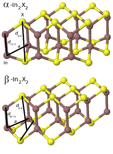
The structures of two stable or metastable polytypes of monolayer hexagonal In2X2 identified in this work are shown in Fig. 1. Viewed from above, a monolayer of -In2X2 forms a 2D honeycomb lattice, with vertically aligned In2 and X2 pairs at the different sublattice sites. Its point group is . The orbitals of the In atoms in each dimer are strongly hybridized, and each of the two In atoms is bound to three neighboring chalcogens. The lattice structure of -In2X2 is depicted in the bottom panel of Fig. 1, with one of the X layers shifted with respect to the other, breaking the mirror symmetry of the original structure but establishing inversion symmetry in its stead. The point group of -In2X2 is . The lattice parameters calculated using ab initio density functional theory (DFT) for these two polytypes of In2X2 are discussed in Sec. II, along with lattice dynamics. We find that the and polytypes can be distinguished by comparing optically active [infrared (IR) and Raman] phonon spectra and that the band structures of -In2X2 crystals are very similar to those of hexagonal Ga2X2 crystals.ZolyomiGaX In Secs. III and IV we report first-principles calculations of the electronic band structures of -In2X2 and -In2X2.
Our DFT calculations were performed using the castepcastep and vaspvasp plane-wave-basis codes to calculate the structural parameters of In2X2. We used both the local density approximation (LDA) and the Perdew-Burke-Ernzerhofpbe (PBE) generalized gradient approximation exchange-correlation functionals in our calculations. The same functionals were used to calculate the electronic band structures, optical absorption spectra, and phonon dispersion curves. For the electronic band structures we also used the screened Heyd-Scuseria-Ernzerhof 06 (HSE06) hybrid functionalhse to compensate at least partially for the underestimation of the band gap by the LDA and PBE functionals. The HSE06 band structure calculations used the geometry optimized using the PBE functional. The plane-wave cutoff energy used in our calculations was 600 eV. During the geometry relaxations a Monkhorst-Pack k-point grid was used, while band structures were obtained with a grid. The optical absorption spectra were obtained with a very dense grid of k points. The artificial out-of-plane periodicity of the monolayer was set to 20 Å in each case. Phonon dispersion curves were calculated in vasp using the method of finite displacements in a supercell with k-points, and in castepcastep2 using density functional perturbation theory (DFPT). We also evaluated the infrared intensity and Raman intensity tensors for the zone-center optical phonons in In2X2. The DFPT calculations used a plane-wave cutoff of 816 eV, a Monkhorst–Pack grid, norm-conserving DFT pseudopotentials, and an artificial periodicity of 15.9 Å.
II Lattice structure and lattice dynamics of -In2X2 and -In2X2
II.1 Lattice structures
Our geometry-optimization calculations show that the lattice parameters in -In2X2 increase with the atomic number of the chalcogen atom X, while the In–In bond lengths hardly change: see Table 1. The bond lengths obtained with the PBE functional are systematically larger than those optimized within the LDA, as expected.FavotF_1999 As shown in Sec. II.2, we find all three -In2X2 crystals to be dynamically stable. The cohesive energy is also shown in Table 1. This is the energy of two isolated indium atoms plus the energy of two isolated chalcogen atoms minus the energy per unit cell of the In2X2 layer. We have not included the zero-point phonon energy in the latter. The difference between the LDA and PBE cohesive energies is significant; nevertheless, both functionals predict the cohesive energy to be largest for In2S2 and smallest for In2Te2.
| -In2X2 | ||||||||||
|---|---|---|---|---|---|---|---|---|---|---|
| (Å) | (Å) | (Å) | (eV/cell) | ZPE (eV/cell) | ||||||
| X | LDA | PBE | LDA | PBE | LDA | PBE | LDA | PBE | LDA | PBE |
| S | ||||||||||
| Se | ||||||||||
| Te | ||||||||||
| -In2X2 | ||||||||||
| (Å) | (Å) | (Å) | (eV/cell) | ZPE (eV/cell) | ||||||
| X | LDA | PBE | LDA | PBE | LDA | PBE | LDA | PBE | LDA | PBE |
| S | ||||||||||
| Se | ||||||||||
| Te | ||||||||||
We have also performed calculations to investigate the -In2X2 polytypes. We find that these structures are dynamically stable, but the static-lattice cohesive energy is slightly lower than the structure by 0.022 and 0.013 eV per unit cell according to the LDA and PBE functionals, respectively. The relative energy of the and polytypes is almost the same for each chalcogen X. The phonon zero-point energies (ZPEs) reported in Table 1 demonstrate that lattice dynamics does not affect the relative stability of the and polytypes. The optimal lattice parameters of these structures are summarized in the bottom half of Table 1.
II.2 Lattice dynamics
| -In2X2 | ||||||||
|---|---|---|---|---|---|---|---|---|
| (cm-1) | IR intensity (D2Å-2amu-1) | Polarization of Raman- | ||||||
| Branch | In2S2 | In2Se2 | In2Te2 | Irrep. | In2S2 | In2Se2 | In2Te2 | active modes |
| 4 | – | – | – | |||||
| 5 | – | – | – | |||||
| 6 | – | – | – | |||||
| 7 | – | – | – | |||||
| 8 | – | – | – | |||||
| 9 (TO) | () | 5.18 | 3.57 | |||||
| 10 (LO) | () | 5.18 | 3.57 | |||||
| 11 (ZO) | () | 0.10 | 0.061 | – | ||||
| 12 | – | – | – | |||||
| -In2X2 | ||||||||
| (cm-1) | IR intensity (D2Å-2amu-1) | Polarization of Raman- | ||||||
| Branch | In2S2 | In2Se2 | In2Te2 | Irrep. | In2S2 | In2Se2 | In2Te2 | active modes |
| 4 | 40.8 | 35.8 | 31.2 | – | – | – | ||
| 5 | 40.8 | 35.8 | 31.2 | – | – | – | ||
| 6 | 134 | 106 | 84.9 | – | – | – | ||
| 7 | 261 | 177 | 146 | – | – | – | ||
| 8 | 261 | 177 | 146 | – | – | – | ||
| 9 (TO) | 262 | 180 | 149 | 10.4 () | 5.4 | 3.8 | – | |
| 10 (LO) | 262 | 180 | 149 | 10.4 () | 5.4 | 3.8 | – | |
| 11 (ZO) | 281 | 198 | 161 | 0.25 () | 0.10 | 0.06 | – | |
| 12 | 293 | 228 | 207 | – | – | – | ||
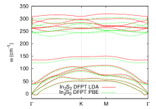
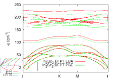
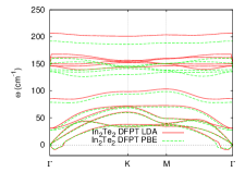
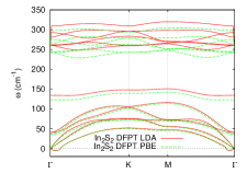
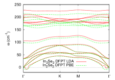
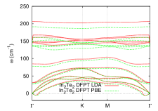
We have calculated phonon dispersion curves for In2X2 using both the finite-displacement approach and DFPT. The DFPT results are presented in Fig. 2. The finite-displacement approach agrees very well with these dispersion curves at a supercell size of primitive unit cells. Other than a small pocket near , we find no trace of imaginary frequencies in the Brillouin zone. This small pocket of instability (shown in detail in the inset beside the middle panel of Fig. 2 for -In2Se2) is extremely sensitive to the details of the calculation and in some cases disappears altogether. This suggests that it merely indicates the difficulty of achieving numerical convergence for the flexural phonon branch, which appears to be a common issue in first-principles calculations for 2D materials.footnote:instability Therefore the phonon dispersion curves suggest that isolated atomic crystals of hexagonal indium chalcogenides, In2X2, are dynamically stable. The spurious imaginary modes were assumed not to contribute to the ZPEs reported in Table 1. The nonanalytic contribution to the dynamical matrix due to long-range Coulomb interactions (longitudinal/transverse optical mode splitting) is neglected in this work. For a discussion of this issue in 2D materials, see App. A of Ref. sanchez-portal, .
The DFT-LDA phonon dispersions for - and -In2X2 are shown in Fig. 2. The caption for this figure also contains a tabulated list of all IR- and Raman-active optical phonon modes at the point. We have used a unit cell with lattice vectors and , where is the lattice parameter. The lattice parameters and other structural parameters are given in a separate Table 1. , , and are unit vectors in the Cartesian directions. The most important difference between the and structures is the number of Raman-active -point phonons. We find that there are two fewer Raman-active modes in -In2X2, offering a way to distinguish the polytypes. Note that -In2X2 possesses inversion symmetry, while -In2X2 does not. Raman and IR activity are mutually exclusive in materials with inversion symmetry. If none of the IR-active modes found in In2X2 appears in the Raman spectrum of a sample, this would point towards the -In2X2 polytype. We discuss the electronic band structure of the energetically more favorable phase in Sec. III, and then discuss the phase in Sec. IV.
III Electronic and optical properties of monolayers of -In2X2
III.1 Band structures
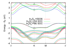
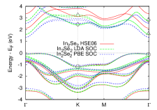
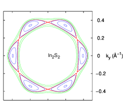
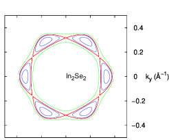
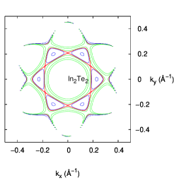
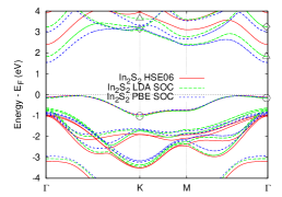
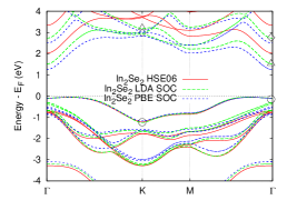
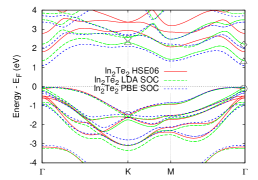
The calculated electronic band structures of -In2X2 are summarized in Fig. 3, with the orbital compositions and spin–orbit splittings tabulated in the figure caption. All three materials are indirect-gap semiconductors, primarily due to the valence-band maximum (VBM) lying between the and K points. Further analysis of the valence band reveals a saddle point along the –M line, illustrated in Fig. 4. This saddle point gives rise to a Van Hove singularity in the density of states. Due to the presence of these saddle points, hole-doping causes In2X2 to undergo a Lifshitz transition when the hole concentration reaches the critical value where all states are depleted above the energy of the saddle point, since this leads to a change in the topology of the Fermi surface. The carrier density at which the Lifshitz transition takes place in each material is tabulated in the caption of Fig. 4 and was obtained by integrating the DFT density of states from the saddle point to the valence-band edge.
It is possible to fit an inverted sombrero polynomial to the valence-band dispersions around the VBM:
| (1) |
where and are the radial and polar coordinates of wave vectors about the point. The polar angle is measured from the –K line. The parameters and were obtained by fitting Eq. (1) to the DFT valence band in the ranges Å Å-1, Å Å-1, and Å Å-1 in In2S2, In2Se2, and In2Te2, respectively. The fitting ranges are centered on the position of the VBM and their widths are chosen to ensure a quantitatively accurate fit at both the VBM and the saddle point. The coefficients are tabulated in the caption of Fig. 4. This fit should provide a good starting point for a simple analytical model of the valence band in these materials. Note, however, that the fit is designed to describe the immediate vicinity of the VBM and the saddle point, and is of limited accuracy at the point; this is due to the fact that the quality of the fit would drop significantly if we were to extend the fitting range as far as the point. The fitting was performed using the same procedure as that used in Ref. ZolyomiGaX, .
| X | Band | K | (meV) | ||
|---|---|---|---|---|---|
| S | |||||
| S | |||||
| S | |||||
| Se | |||||
| Se | |||||
| Se | |||||
| Te | |||||
| Te | |||||
| Te |
| X | (meV) | ( cm-2) | |||||
|---|---|---|---|---|---|---|---|
| S | |||||||
| Se | |||||||
| Te |
We find that the conduction-band minimum (CBM) is at the point in all cases except the LDA band structure of -In2Te2, where it is at the M point. The HSE06 band structure is expected to be the most reliable and hence we predict that the CBM occurs at in all cases. Nevertheless, there are local minima of the conduction band at , K, and M in each case, with the exception of the PBE band structure of -In2Te2. The HSE06 band gaps of -In2X2 are summarized in Table 2. The HSE06 band gap is expected to underestimate the quasiparticle band gap by no more than 10%,hse10percent and is known to be accurate in 2D materials.hse10scuseria The effective masses at the high-symmetry points in the conduction band are summarized in Table 2. The effective mass is isotropic at the and K points, but not at M. We note that the effective mass is quite sensitive to the fitting range. The data in Table 2 were obtained by fitting in one dimension in a range corresponding to of the K–M line in the Brillouin zone.footnote:mass_fitting If the fitting range is doubled, the effective masses change by up to 10%.
| X | (eV) | Kc | M | M | |
|---|---|---|---|---|---|
| -In2X2 | |||||
| S | 2.53 | ||||
| Se | 2.16 | ||||
| Te | 2.00 | ||||
| -In2X2 | |||||
| S | 2.45 | – | |||
| Se | 2.07 | – | |||
| Te | 1.88 | – | |||
The band structures computed using semilocal density functionals are also plotted in Fig. 3 for comparison. The LDA and PBE functionals give very similar results to the HSE06 functional up to the Fermi level, but above that significant discrepancies arise. This is most notable in the case of -In2Te2, where the position of the CBM is ambiguous: the LDA predicts that the CBM is at the M point, while the PBE functional puts it at the point, in agreement with HSE06. A similar behavior was found in 2D hexagonal gallium chalcogenides.ZolyomiGaX
In the semilocal DFT calculations we took spin-orbit (SO) coupling into account using a relativistic DFT approach.vasp As can be seen in Fig. 3 (also listed in its caption), some of the bands exhibit spin splitting, including the highest valence () and lowest conduction () bands near the K point (see the table in Fig. 3). While we were unable to calculate the SO splittings in HSE06 due to limited computational resources, we expect that they will exhibit a similar magnitude to that found in the semilocal band structures. The caption of Fig. 3 also contains lists describing the orbital decomposition of the valence and conduction band states at the and K points into the most relevant atomic orbitals of In and the chalcogens.
III.2 Optical absorption spectra
The orbital composition of the bands was obtained by projecting the orbitals in the plane-wave basis set of vasp onto spherical harmonics, and the results are reported in the caption of Fig. 3. We have found that these bands around the Fermi level are dominated by - and -type orbitals. Although one expects the orbitals to substantially influence the electronic structure in In-based compounds, the valence and conduction bands of In2X2 monolayers do not appear to contain any significant contributions from states, despite the explicit inclusion of all the electrons in our calculations. States in each band are either odd or even with respect to symmetry (this information is obtained from the complex phases of the orbital decomposition in vasp). Therefore, the interband absorption selection rules require that photons polarized in the plane of the 2D crystal are absorbed by transitions between bands whose wave functions have the same symmetry (eveneven and oddodd), and photons polarized along the axis cause transitions between bands with opposite symmetry (evenodd and oddeven).
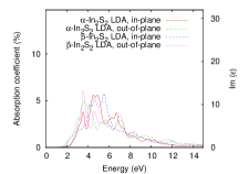
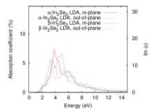
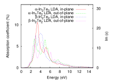
The calculated LDA optical absorption spectra are shown in Fig. 5. The intensities are obtained from the imaginary part of the dielectric function and normalized to absolute units by using graphene as a benchmark,ZolyomiGaX since we know that graphene absorbs 2.3% of light intensity over a broad spectral range. We calculated the LDA dielectric function of graphene at low energies and rescaled the absorption coefficients to reproduce the 2.3% absorption, then applied the same scaling to the In2X2 spectra. Note that LDA results are only qualitatively accurate and should only be used for a comparative study of the different In2X2 monolayers and for an order-of-magnitude estimate of the expected peak positions. Furthermore, local-field effects, which are expected to influence out-of-plane absorption, are not included. A better description would require a computationally much more expensive calculation using the approximation and the Bethe–Salpeter equation for excitonic corrections.bse_example Much like Ga2X2 monolayers, In2X2 sheets exhibit a prominent absorption peak (originating from the vicinity of the K point) near 3–5 eV, where the absorption coefficients of In2X2 are comparable to and even exceed that of monolayer and bilayer graphene. As such, we suggest that ultrathin films of InX biased in vertical tunneling transistors with graphene electrodes could be used as an active element for the detection of ultraviolet photons. It is not surprising to find absorptions of a similar order of magnitude in In2X2 and graphene, since both are atomically thin materials.
IV Electronic and optical properties of monolayers of -In2X2
IV.1 Band structures
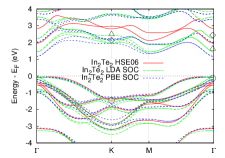
Figure 6 depicts the electronic band structures of -In2X2, which shows that the valence band is strikingly similar to that of the structure in Fig. 3, with the VBM once again between the and K points. This is due to the valence band being dominated by the Ga orbitals, which are in the same configuration in the two polytypes. Unsurprisingly, -In2X2 possesses the same anisotropic sombrero-shaped dispersion as -In2X2 and therefore a Lifshitz transition can be achieved in this case as well. However, the coefficients of the polynomial fit and the critical carrier concentration are quite different, as shown in Table 3. The band structures with SO coupling taken into account are also shown in Fig. 6, with the band wave functions decomposed into the most relevant atomic orbitals of In and the chalcogens listed in the caption.
| X | Band | K | ||
|---|---|---|---|---|
| S | ||||
| S | ||||
| S | ||||
| Se | ||||
| Se | ||||
| Se | ||||
| Te | ||||
| Te | ||||
| Te |
| X | (meV) | ( cm-2) | |||||
|---|---|---|---|---|---|---|---|
| S | |||||||
| Se | |||||||
| Te |
The conduction band of the polytype is similar to that of the polytype near the point; however, some significant differences arise at the K point, where a doubly degenerate band appears at the bottom of the conduction band with a completely different orbital composition from the lowest conduction band of the structure. The orbital composition (see the caption of Fig. 6) of the valence band on the other hand is almost identical to that found in -In2X2.
IV.2 Optical absorption spectra
The optical absorption spectra of -In2X2 are shown in Fig. 5. These show a good deal of similarity to those of -In2X2. The absorption is dominated by a large peak in the ultraviolet range in all cases and the peak absorption exceeds that of graphene.
V Conclusions
We have used DFT to show that 2D hexagonal indium chalcogenides (In2X2 where X is S, Se, or Te) are dynamically stable. We have identified two polytypes of In2X2, and we have shown how these can be distinguished by IR and Raman spectroscopy. We find that all of these materials are indirect-band-gap semiconductors with an unusual inverted-sombrero-shaped valence band. The presence of saddle points in the valence band along the –M line leads to a Lifshitz transition in the event of hole doping, for which we have calculated the critical carrier density. We have provided an analytical fit of the valence-band edge and have given a qualitative description of the optical absorption spectra, which suggest that atomically thin films of InX could find application in ultraviolet photon detectors.
Acknowledgements.
We acknowledge financial support from EC-FET European Graphene Flagship Project, EPSRC Science and Innovation Award, ERC Synergy Grant “Hetero2D,” the Royal Society Wolfson Merit Award, and the Marie Curie project CARBOTRON.References
- (1) K. S. Novoselov, A. K. Geim, S. V. Morozov, D. Jiang, Y. Zhang, S. V. Dubonos, I. V. Grigorieva, and A. A. Firsov, Science 306, 666 (2004).
- (2) A. K. Geim and K. S. Novoselov, Nature Materials 6, 183 (2007).
- (3) Y. Kubota, K. Watanabe, O. Tsuda, and T. Taniguchi, Science 317, 932 (2007)
- (4) M. P. Levendorf, C.-J. Kim, L. Brown, P. Y. Huang, R. W. Havener, D. A. Muller, and J. Park, Nature 488, 627 (2012).
- (5) B. Aufray, A. Kara, S. Vizzini, H. Oughaddou, C. Léandri, B. Ealet, and G. L. Lay, Appl. Phys. Lett. 96, 183102 (2010).
- (6) P. E. Padova, C. Quaresima, C. Ottaviani, P. M. Sheverdyaeva, P. Moras, C. Carbone, D. Topwal, B. Olivieri, A. Kara, H. Oughaddou, B. Aufray, and G. L. Lay, Appl. Phys. Lett. 96, 261905 (2010).
- (7) B. Lalmi, H. Oughaddou, H. Enriquez, A. Kara, S. Vizzini, B. Ealet, and B. Aufray, Appl. Phys. Lett. 97, 223109 (2010).
- (8) N. D. Drummond, V. Zólyomi, and V. I. Fal’ko, Phys. Rev. B 85, 075423 (2012).
- (9) E. Bianco, S. Butler, S. Jiang, O. D. Restrepo, W. Windl, and J. E. Goldberger, ACS Nano 7, 4414 (2013).
- (10) K. F. Mak, C. Lee, J. Hone, J. Shan, and T. F. Heinz, Phys. Rev. Lett. 105, 136805 (2010).
- (11) B. Radisavljevic, A. Radenovic, J. Brivio, V. Giacometti, and A. Kis, Nature Nanotechnol. 6, 147 (2011)
- (12) B. Radisavljevic, M. B. Whitwick, and A. Kis, ACS Nano 5, 9934 (2011).
- (13) T. Georgiou, R. Jalil, B. D. Belle, L. Britnell, R. V. Gorbachev, S. V. Morozov, Y.-J. Kim, A. Gholinia, S. J. Haigh, O. Makarovsky, L. Eaves, L. A. Ponomarenko, A. K. Geim, K. S. Novoselov and A. Mishchenko, Nature Nanotechnol. 8, 100 (2013).
- (14) J. N. Coleman, M. Lotya, A. O’Neill, S. D. Bergin, P. J. King, U. Khan, K. Young, A. Gaucher, S. De, R. J. Smith, I. V. Shvets, S. K. Arora, G. Stanton, H.-Y. Kim, K. Lee, G. T. Kim, G. S. Duesberg, T. Hallam, J. J. Boland, J. J. Wang, J. F. Donegan, J C. Grunlan, G. Moriarty, A. Shmeliov, R. J. Nicholls, J. M. Perkins, E. M. Grieveson, K. Theuwissen, D. W. McComb, P. D. Nellist, and V. Nicolosi, Science 331, 568 (2011).
- (15) C. Ataca, H. Sahin, and S. Ciraci, J. Phys. Chem. C 116, 8983 (2012).
- (16) D. Braga, L. I. Gutiérrez, H. Berger, and A. F. Morpurgo, Nano Lett. 12, 5218 (2012).
- (17) V. Zólyomi, N. D. Drummond, and V. I. Fal’ko, Phys. Rev. B 87, 195403 (2013).
- (18) Chemistry of the Main Group Elements, ed. A. R. Barron, CONNEXIONS, Rice University, Houston, Texas (2010).
- (19) A. Segura, J. Bouvier, M. V. Andrés, F. J. Manjón, and V. Muñoz, Phys. Rev. B 56, 4075 (1997).
- (20) O. Z. Alekperov, M. O. Godjaev, M. Z. Zarbaliev, and R. Suleimanov, Solid State Commun. 77, 65 (1991).
- (21) C. De Blasi, G. Micocci, S. Mongelli, and A. Tepore, J. Cryst. Growth 57, 482 (1982).
- (22) A. Gouskov, J. Camassel, and L. Gouskov, Prog. Cryst. Growth Charact. 5, 323 (1982).
- (23) G. A. Gibson, A. Chaiken, K. Nauka, C. C. Yang, R. Davidson, A. Holden, R. Bicknell, B. S. Yeh, J. Chen, H. Liao, S. Subramanian, D. Schut, J. Jasinski, and Z. Liliental-Weber, Appl. Phys. Lett. 86, 051902 (2005).
- (24) S. Lei, L. Ge, S. Najmaei, A. George, R. Kappera, J. Lou, M. Chhowalla, H. Yamaguchi, G. Gupta, R. Vajtai, A. D. Mohite, and P. M. Ajayan, ACS Nano 8, 1263 (2014).
- (25) G. W. Mudd, S. A. Svatek, T. Ren, A. Patanè, O. Makarovsky, L. Eaves, P. H. Beton, Z. D. Kovalyuk, G. V. Lashkarev, Z. R. Kudrynskyi, and A. I. Dmitriev, Adv. Mater. 25, 5714 (2013).
- (26) A. G. Fitzgerald, Conf. Series IoP 147, 409 (1995).
- (27) S. J. Clark, M. D. Segall, C. J. Pickard, P. J. Hasnip, M. I. J. Probert, K. Refson, and M. C. Payne, Z. Kristallogr. 220, 567 (2005).
- (28) G. Kresse and J. Furthmüller, Phys. Rev. B 54, 11169 (1996).
- (29) J. P. Perdew, K. Burke, and M. Ernzerhof, Phys. Rev. Lett. 77, 3865 (1996).
- (30) J. Heyd, G. E. Scuseria, and M. Ernzerhof, J. Chem. Phys. 118, 8207 (2003); A. V. Krukau, O. A. Vydrov, A. F. Izmaylov, and G. E. Scuseria, ibid. 125, 224106 (2006).
- (31) K. Refson, P. R. Tulip, and S. J. Clark, Phys. Rev. B 73, 155114 (2006).
- (32) F. Favot and A. Dal Corso, Phys. Rev. B 60, 11427 (1999).
- (33) We have observed the existence of small regions of phonon instability in the flexural acoustic (ZA) modes around in graphene, silicene, molybdenum disulfide, and gallium chalcogenides. The region of instability shows extreme sensitivity to simulation parameters such as supercell size and -point sampling. Moreover, the absolute values of the imaginary frequencies are similar to the amount by which the acoustic branches of the dispersion curve miss zero when Newton’s third law is not imposed on the matrix of force constants. For these reasons we believe that these regions of instability are spurious.
- (34) D. Sánchez-Portal and E. Hernández, Phys. Rev. B 66, 235415 (2002).
- (35) S. Park, B. Lee, S. H. Jeon, and S. Han, Current Applied Physics 11, S337 (2011).
- (36) J. K. Ellis, M. J. Lucero, and G. E. Scuseria Appl. Phys. Lett. 99, 261908 (2011).
- (37) To determine the effective mass at the K point, we fitted , where is the distance from the K point, is the polar angle and the are fitting parameters, to our energy bands along the K– and the K–M lines. At the point we used a similar procedure, but with a fitting function . At the M point, where the effective mass is anisotropic, we fitted separately along the M– and M–K directions to obtain the effective masses along the two principal axes of the effective mass tensor.
- (38) G. Onida, L. Reining, and A. Rubio, Rev. Mod. Phys. 74, 601 (2002).