Exciton Binding Energy of Monolayer WS2
Abstract
The optical properties of monolayer transition metal dichalcogenides (TMDC) feature prominent excitonic natures. Here we report an experimental approach toward measuring the exciton binding energy of monolayer WS2 with linear differential transmission spectroscopy and two-photon photoluminescence excitation spectroscopy (TP-PLE). TP-PLE measurements show the exciton binding energy of 0.710.01eV of the band-edge excitons around K valley in the Brillouin zone.
pacs:
78.66.-w 73.22.-f 78.20.-e 78.67.PtCoulomb interactions are significantly enhanced in low dimensional systems as a result of spatial confinement and reduced screening, and consequently excitons, quasiparticles of electron-hole pairs bounded by Coulomb force play a pronounced role in their optical aspects. A few paradigms of the pronounced excitonic effects have been demonstrated in quantum dots and carbon nanotubes where the exciton binding energies are found to be a fraction of their band gaps in these quasi-zero dimensional (0D) and one dimensional (1D) systems. Prominent exciton effects are also widely expected in intrinsic 2D systems for instance monolayer crystals of transition metal dichalcogenides (TMDC) owing to the reduced dielectric screening and spatial confinementkey-1 (1, 2). Monolayer TMDC is an intrinsic 2D crystal consisting of two hexagonal planes of chalcogen atoms and an intermediate hexagonal plane of metal atoms in a prismatic unit cell. Particularly MX2 (MoS2, MoSe2, WS2 and WSe2) experiences a transition from indirect gap in bulk form to direct gap of visible frequency in monolayers, where the band gap is located at K(K’) valley of the Brillouin zonekey-3 (3, 4, 5, 6). Ab initio calculations show the direct-gap exciton binding energy in the range of 0.5-1eV which is around 1/3-1/2 of the corresponding optical direct gapkey-1 (1, 2, 7, 8). The modulated absorption/reflection spectroscopy shows the binding energy of direct gap excitons around 55meV in bulk crystalsbulkcrystal_ref . Such a big exciton binding energy in bulk form guarantees the robust excitonic nature of optical properties in ultrathin counterparts. Furthermore, photoluminescence (PL) experiments identify electron(hole)-bounded excitons, so called trions, with a charging energy of 18meV, 30meV and 20-40meV in monolayer MoS2, MoSe2 and WS2 respectivelytrion-mose2 ; trion_mos2 ; trion-WS2 . With a simple 2D exciton model, one could estimate the exciton binding energy around 10 times that of the trion, if equal effective electron’s and hole’s mass are assumedtrion-model . As yet the direct measurement of exciton binding energy in monolayer TMDC is lacking.
Here we report experimental approaches toward measuring the exciton binding energy of monolayer WS2 with linear differential transmission spectroscopy and two-photon photoluminescence excitation spectroscopy (TP-PLE). The TP-PLE resolves the excited states of excitons and the interband transition continuum. The exciton binding energy of 0.710.01eV of the band-edge excitons around K valley in the Brillouin zone is extracted by the energy difference between the ground state exciton and the onset of the interband continuum.
Monolayer WS2 was mechanically exfoliated from single crystal WS2 and identified with optical microscope and photoluminescence spectroscopy (supplementary information). The samples in differential transmission measurements were made by transferring from silicon substrates to freshly cleaved mica substrates as described in Reftransfer . The electric gate dependent PL measurements were carried out with a field effect transistor structure on silicon wafers with a 300nm oxide cap layer. The TP-PLE spectroscopy was carried out with a confocal setup with a 20X achromatic objective and a Ti:sapphire oscillator (80MHz, 100fs).
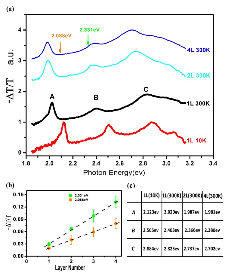
Figure 1a summarizes linear optical measurements of monolayer and multilayer WS2. There are distinct peaks in the differential transmission spectra, labeled as “A”, “B” and “C” respectivelykey-6 (6, ). Peaks “A” around 2eV and “B” around 2.4eV at room temperature present the excitonic absorptions at the direct gap located at K valley of the Brillouin zones. The separation between “A” and “B” of 0.38eV rising from the splitting of valence band minimum (VBM) due to spin-orbit coupling (SOC) at K(K’) valley is almost constant in all the layers with various thickness, consistent with the PL spectrakey-6 (6, 5). It is the direct result of the suppression of interlayer coupling at K(K’) valley owing to the giant SOC and spin-valley coupling in tungsten TMDC with 2H stacking order in which each unit layer is a rotation of its adjacent layerskey-5 (5). The peak “C” around 2.8eV was recognized as the excitonic transitions from multiple points near point of the Brillouin zonekey-2 (2, ). Unlike in many semiconductors, the linear absorption spectra of WS2 display no gap between distinct excitons and the continuum of interband transitions. The continuous absorption originates from the strong electron(hole)-phonon coupling in TMDCs and the efficient phonon scattering fills the gap between the ground state excitons and the interband continuum in the linear absorption spectrakey-2 (2). As the temperature drops to 10K, the peak “A” and “B” are both blue-shifted by around 0.1eV and peak “C” is shifted by 0.06eV as shown in Figure 1c. The difference of the blue-shift is the direct consequence of the diverse locations of the excitons in the Brillouin zone: exciton “A” and “B” are formed at K valley while “C” is around point. Nevertheless, the continuous absorption still survives and no distinct single-particle band edge emerges at cryogenic temperature (10K). The linear absorption spectra cannot resolve the exciton binding energy.
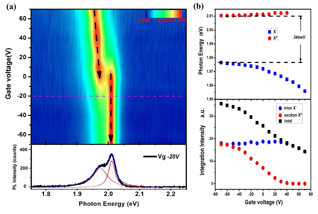
Figure 1b shows the absorbance of WS2 atomically thin films as a function of the thickness above their ground exciton energy, which is approximated with the differential transmission. The absorbance of monolayer and multilayers is linearly proportional to their thickness, each layer absorbing around 2.0% and 3.4% at excitations of 2.088eV and 2.331eV respectively. The linear layer dependence of the absorption gives an experimental evidence of the suppression of interlayer hopping in 2H stacked WS2 as a result of spin-valley couplingkey-5 (5, ). The thickness dependence could also be used as a thickness monitor for multilayer/monolayer characterization. There is a side bump at the red side of exciton A, which modifies the lineshape away from the symmetric Lorentzian or Gaussian shape. We tentatively attribute the bump to the effect of electron/hole bound exciton or triontrion-mose2 ; trion-WS2 ; trion_mos2 . Although the monolayer WS2 is not intentionally doped, the structural defects and substrate effects such as charge transfer and defects modulate the carrier density away from its insulating state. To confirm the origin of the bump around exciton A, we record the PL spectra of monolayer WS2 at various electric gating (from 70V to -70V) which continuously tunes the Fermi level of monolayer WS2 as illustrated in figure 2a.
There is a prominent peak X- at the red side of the free exciton X0 at and the PL spectrum could be described by a superposition of two Lorentzian curves which center at peak X0 and X- respectively as illustrated in figure 2b. As the gate voltage goes towards positive values (Vg>0), the free exciton X0 gradually diminishes and disappears at Vg>40V. Meanwhile the red-side X- rises to take over the overwhelming weight of the whole PL until starts to decrease at Vg>20V probably due to the electrostatic screening effectkey-20 , and the peak X- is further red-shifted. The electric gating dependence attributes X- to n-type trion (electron-bounded exciton) states. As Vg goes to negative bias , the free exciton state X0 takes over the weight of the PL and tends to saturate around Vg=-70V. While the trion state X- monotonically diminishes, the redshift also shows a sign of saturation of -34meV at around Vg=-70V. This confirms the trion (electron-bound exciton) origin of the side bump around exciton A in the monolayer transmission spectrum and the trion binding energy of 34meV in monolayer. If we follow the simplified trion model in conventional quantum wellstrion-model and take the effective mass of either me=0.37 and mh=-0.48key-21 or me=0.27,mh=-0.32key-7 (7), the binding energy of free exciton is estimated at .
Two-photon excitation is a third order optical process involving simultaneous absorption of the two photons which follows selection rules different from those in one-photon (linear) process. As a photon has an odd intrinsic parity, one- and two-photon transitions are mutually exclusive in systems with inversion symmetry : one-photon transitions are allowed between states with different parity and two-photon transitions between states with the same parity; in systems without inversion symmetry like monolayer TMDCs described by a point group of D3h symmetry, parity is not a good quantum number and there exist transitions which are both one- and two-photon allowed. Nevertheless, the oscillator strengths of exciton states are generally different between one- and two-photon processes. A simplified exciton model could be described as where ( presents the electron (hole) wave function, and is the function of relative motion of electron-hole. The optical transition rates for one- and two-photon processestwo-photon
where A denotes the vector potential of the excitation, the light polarization unit vector, the interband matrix elements, and the line-shape function of interband exciton. In a 2D system, could be described by a solution of 2D Wannier-Mott exciton and the exciton binding energy could be described as where n=1,2… is the principle quantum number, l=0,1,..(n-1) is the angular quantum number, and is the associate Laguerre polynomial. As the exciton oscillator strength decays as , only the ground state (n=1) and the first two excited states are considered. In a one-photon process, the ground state 1s (n=1,l=0) dominates; Whereas in a two-photo process the ground state and ns states (l=0) are dramatically subsidized owing to and the p state dominates. Analyzing the difference between one- and two-photon processes would lead to extracting the exciton binding energy of monolayer TMDC.
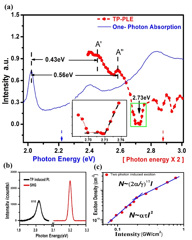
Figure 3 shows a TP-PLE spectrum of monolayer WS2, where the PL intensity of free band-edge exciton A is recorded as a function of the pulsed excitation energy. With the contrasting optical transition strength, two-photon excitation resonant with p type exciton states dominates while s type is nearly invisible. The prominent PL occurs at the excitation around 1.2eV which is the half of the exciton B energy and 1.29eV. There is a significant gap state in the range of 1.35-1.36eV where the PL intensity drops to nearly negligible. The negligible but nonzero PL intensity likely results from the re-absorption of the second harmonic excitation, since the SHG intensity is more than one order of magnitude higher than that of two-photon luminescence as shown in Figure 3b. Upon the excitation just above the gap (> 1.365eV) as indicated by the arrow in Figure 3a, the PL intensity shows a linear increase with the excitation energy as indicated in the inset. It is the signature of two-photon absorption with in-plane polarization in 2D systemtwo-photon . Besides, the two local minimums at higher excitation energy around 1.44eV and 1.46eV have significant PL intensity and therefore are unlikely to be the single-particle band gap state. Thus the single-particle gap could be determined at 2.73eV (2X1.365eV), consistent with RefYe . Given that the PL peaks at 2.02eV presenting the energy of the ground-state exciton, the exciton binding energy of is extracted from the energy difference between the ground-state exciton and the onset of the inter-band continuum.
With the band-edge exciton binding energy of 0.71eV we could attribute the peaks around 2.42eV (2X1.21eV) and 2.58eV (2X1.29eV) in the TP-PLE spectrum to the excited states of excitons, which are qualitatively consistent with the recent ab initio calculationYe . As the exciton A and B both originate from the spin-split valence bands at K(K’) valley with the similar effective mass, a similar strength of binding energy is expected. Besides, the PL intensity around the peak A’ and A” monotonically decreases. Both peaks are likely to be the excited state of the same exciton, and we tentatively attribute peaks A’ and A” to the 2p and 3p states of exciton A respectively. The exciton binding energy could also be evaluated from the energy difference between exciton 1s and np states. The 2D hydrogen model gives the energy difference between 1s and 2p(3p)
which correspond to and respectively. The alternative assignment for example peak A’ to 3p state leads to . These are significantly smaller than extracted from the energy difference between the ground state exciton and the onset of the inter-band continuum, and the distribution of these excited states also significantly deviates from that of the 2D hydrogen model. The difference may lie in the modification of the 2D hydrogen model by electron-phonon and electron correlation interactions in monolayer TMDC. Recent first principle simulation shows that q-dependent screening dramatically enhances the binding energy of the excited states of excitonskey-2 (2, ). Nevertheless, it is safe to extract the exciton binding energy of by the energy difference between 1s exciton and the onset of the interband continuum, independent of the assignments of the excited states. It also implies that the model to estimate the exciton binding energy via trion binding energy is inappropriate.
The two-photon absorption has a quadratic dependence on the excitation intensity in principle. The two-photon photoluminescence (TP-PL) intensity from monolayer WS2 displays a clear quadratic dependence on the excitation intensity at low power as shown in figure 3c. As the excitation intensity increases above , the PL intensity experiences a clear transition from quadratic to linear dependence on the excitation intensity. If we follow the simple model
where N denotes the exciton density, I the excitation intensity, the two-photon absorption cross section, the exciton lifetime and the exciton-exciton annihilation rate, the fitting of the quadratic dependence () gives two-photon absorption cross section of at 1.59eV where the PL quantum yield of key-3 (3) and the exciton lifetime of 100ps are assumedJF . Subsequently the linear dependence slope at high intensity yields the exciton-exciton annihilation rate which is qualitatively consistent with that in monolayer MoSe2 measured by pump-probe reflection spectroscopyzhaohui . The linear intensity dependence of TP-PL is the evidence of the strong exciton-exciton interactions in monolayer TMDCs.
In summary, the linear absorption spectroscopy cannot resolve the electronic interband transition edge down to 10K due to the strong electron-phonon scattering and the overlap of excitons around point. The TP-PLE measurements successfully probe the excited states of the band-edge exciton and the single-particle band gap. The exciton binding energy of 0.710.01eV is extracted by the energy difference between 1s exciton and the single-particle gap in monolayer WS2. The distribution of the exciton excited states significantly deviates from the 2D hydrogen model. The giant exciton binding energy manifests the unprecedented strong Coulomb interactions in monolayer TMDCs.
References
- (1) T. Cheiwchanchamnangij and W. R. L. Lambrecht, Physical Review B 85, 205302 (2012).
- (2) D. Y. Qiu, F. H. da Jornada, and S. G. Louie, Physical Review Letters 111, 216805 (2013).
- (3) K. F. Mak, C. Lee, J. Hone, J. Shan, and T. F. Heinz, Physical Review Letters 105, 136805 (2010)
- (4) A. Splendiani, L. Sun, Y. Zhang, T. Li, J. Kim, C.-Y. Chim, G. Galli, and F. Wang, Nano Letters 10, 1271 (2010).
- (5) H. Zeng et al., Sci. Rep. 3 (2013)
- (6) W. Zhao, Z. Ghorannevis, L. Chu, M. Toh, C. Kloc, P.-H. Tan, and G. Eda, ACS Nano 7, 791 (2012).
- (7) H. L. Shi, H. Pan, Y. W. Zhang, and B. I. Yakobson, Physical Review B 87, 155304(2013).
- (8) A. Ramasubramaniam, Physical Review B 86, 115409 (2012).
- (9) A. A. Mitioglu, P. Plochocka, J. N. Jadczak, W. Escoffier, G. L. J. A. Rikken, L. Kulyuk, and D. K. Maude,Phys. Rev. B 88, 245403(2013)
- (10) J. Bordas, Some Aspects of Modulation Spectroscopy in Optical and electrical properties (Springer, 1976), pp. 145.
- (11) K. F. Mak, K. He, C. Lee, G. H. Lee, J. Hone, T. F. Heinz, and J. Shan, Nat Mater 12, 207 (2013).
- (12) J. S. Ross et al., Nat Commun 4, 1474 (2013).
- (13) A. Thilagam, Physical Review B 55, 7804 (1997).
- (14) A. Reina, H. Son, L. Jiao, B. Fan, M. S. Dresselhaus, Z. Liu, and J. Kong. J. Phys. Chem. C. 112, 17741 (2008).
- (15) A. Shimizu, T. Ogawa, and H. Sakaki, Physical Review B 45, 11338 (1992).
- (16) Z. Ye, T. Cao, K. O’Brien, H. Zhu, X. Yin, Y. Wang, S. G. Louie and X. Zhang, arXiv:1403.5568
- (17) T. Ando, Y. Zheng, and H. Suzuura, Journal of the Physical Society of Japan 71, 1318 (2002).
- (18) Z. Gong, G.-B. Liu, H. Yu, D. Xiao, X. Cui, X. Xu, and W. Yao, Nat Commun 4 (2013).
- (19) S. Tongay et al., Nano Letters 13, 2831 (2013).
- (20) D. Xiao, G.-B. Liu, W. Feng, X. Xu, and W. Yao, Physical Review Letters 108, 196802 (2012).
- (21) N. Kumar, Q. Cui, F. Ceballos, D. He, Y. Wang and H. Zhao, arXiv:1311.1079
- (22) B. Zhu, H. Zeng, J. Dai,Z. Gong and X. Cui, ArXiv:1403.6224