Mechanical Strain can Switch the Sign of Quantum Capacitance from Positive to Negative
Abstract
Quantum capacitance is a fundamental quantity that can directly reveal many-body interactions among electrons and is expected to play a critical role in nanoelectronics. One of many tantalizing recent physical revelations about quantum capacitance is that it can posses a negative value, hence allowing for the possibility of enhancing the overall capacitance in some particular material systems beyond the scaling predicted by classical electrostatics. Using detailed quantum mechanical simulations, we find an intriguing result that mechanical strains can tune both signs and values of quantum capacitance. We use a small coaxially-gated carbon nanotube as a paradigmatical capacitor system and show that, for the range of mechanical strain considered, quantum capacitance can be adjusted from very large positive to very large negative values (in the order of plus/minus hundreds of attofarads), compared to the corresponding classical geometric value (0.31035 aF). We elucidate the mechanisms underpinning the switching of the sign of quantum capacitance due to strain. This finding opens novel avenues in designing quantum capacitance for applications in nanosensors, energy storage, and nanoelectronics.
pacs:
73.22.-f, 73.63.-b, 84.32.TtThe behavior of nanoscale capacitors is remarkably rich and exhibits features unanticipated by conventional electrostatic theory Buttiker93 ; Spaldin06 ; Spaldin09 . Intense research activity has recently ensued on materials development, elucidation of the fundamental science and applications related to nano capacitors. Conventional wisdom, with its origins in text-book electrostatics, suggests that high capacitance can be achieved by reducing the characteristic size of the dielectric materials with high dielectric permittivity. For example, in the case of a thin film configuration, the classical electrostatic capacitance per unit area is taken to be where is the dielectric permittivity and is the thickness of the dielectric sandwiched between the electrodes. Accordingly, materials development have tended to focus on the selection and engineering of high dielectric permittivity materials at the nanoscale along with the concomitant challenges of their fabrication and testing. Unfortunately, experiments have shown that in many thin and high-permittivity insulators (such as Ta2O5), their capacitance values are orders of magnitude smaller Mead61 ; Saad04 ; Boesch08 —compared to what may be expected from classical electrostatics. Using ab inito calculations and many-body quantum theory, this perplexing discovery has been explained in part by the existence of the atomically thin two-dimensional electron gas (2DEG) between the insulators and the metallic gates Spaldin06 ; Spaldin09 ; Kopp09 . The electron accumulation at such interfaces is due to the imperfect screening at the metallic interface, causing an extraneous contribution to overall capacitance, termed quantum capacitance. In the metallic (gate)-insulator-metallic (gate) setup, the quantum capacitance is incorporated into a series capacitor model as:
| (1) |
Here is the capacitance measured by mounting leads to an external voltmeter, is the classical geometric capacitance obtained from electrostatic principles, and is the aforementioned quantum capacitance. In general is many orders of magnitude greater than the geometric capacitance , hence its effects in sub-micron or larger scales are nearly nonexistent. can be only realized in nanoscale or in devices containing high-dielectric materials.
Despite having been identified for nearly three decades Luryi88 , quantum capacitance has only gained much interest for in recent years Ilani06 ; Li11 ; Liu12 ; Yu13 . From first-principles viewpoint, quantum capacitance arises from many-body interactions among electrons, and it relates to the change in electron density with the chemical potential of the 2DEG as
| (2) |
Contributions to stems from density of states, and exchange/correlation energy functional of the 2DEG. At a glance, it may seem as if quantum capacitance will always tend to diminish the overall capacitance . However, due to the negative exchange-correlation contribution, quantum capacitance can very well enhance the overall capacitance. Recently, a few materials systems have been identified in experiments as plausible realization of this enhancement effects. Examples include C-CuO2-Cu coaxial nanowires and LaAlO3/SrTiO3 films system where about % and 40% enhancement of capacitance have been reported respectively Li11 ; Liu12 .
A number of quantitative effects, including the finite thickness of the two-dimensional sheets, interface reconstruction, among many others can influence quantum capacitance Kopp09 . We report here a surprising aspect of the quantum capacitance pertaining to mechanical deformation. This notion may be motivated by considering a 2DEG in low-electronic density limit. A dimensionless distance may be defined as where is the total carrier density. This distance characterizes the inter particle distances which directly depend on the amount of applied strain. Using this argument, we rationalize that mechanical strain should alter the electronic densities, and the exchange contribution to quantum capacitance. Although existing studies have already established the fundamental science underlying quantum capacitance Giuliani05 ; Fogler05 ; Kopp09 ; Kusminskiy08 ; Borghi10 , the potential role of mechanical effects remains unexplored.
In this Letter, we explore the possibility of tuning quantum capacitance (hence the overall capacitance ) via mechanical strain. We find that, for a model system based on carbon nanotube, in conjunction with appropriate doping levels, mechanical strain can indeed substantially change the values of quantum capacitance and more intriguingly, switch its sign from positive to negative (and vice versa).
The model configuration is shown in Fig. 1(a). A (10,0) nanotube is coaxially gated by a metallic stripe. The stripe is separated from the nanotube by a SiO2 insulator with the relative permittivity of . All features are placed inside a Poisson box where the electronic charge and potential is solved self-consistently. Two metallic planes act as a grounded reference contacts which serve as source/drain of electrons in response to applied fields of the cylindrical gate.
Quantum capacitance has been obtained using a combination of Density Functional Tight-Binding Theory (DFTB) and methods in nonequilibrium Green’s functions (NEGF)—the details related to the specific computational code may be found in Refs. Aradi07 ; Pecchia04 ; DiCarlo05 . The exchange-correlation (XC) contribution to the total electronic energy is approximated by the Hubbard model. The carbon-carbon interactions are those provided in the Slater-Koster parameter set in Latessa05 , and PBC-0-1 Rauls99 . The DFTB+NEGF package used Aradi07 has been modified to allow for the aforementioned coaxially gated nanotube configuration. The underlying principles of the setup will become clear in a moment. Emphasizing first on model description, the nanotube considered contains 2,160 atoms and has about 22.6 nm in length. It has been coaxially gated by a hollow metallic cylindrical stripe located at a distance about 11.1 Å away. The separating insulator gives rise to the regular geometric capacitance () as expected. Dirichlet boundary conditions have been enforced on the metallic planes to simulate grounded contacts at source and drain. The same boundary condition is also used to apply a constant voltage at the cylindrical metallic gate. The source/drain outside of the Poisson box are used for induced charge accumulation (or depletion) at the surface of the nanotube which is treated within the NEGF framework. Our geometric set up follows ones in Latessa05 ; Latessa07 .
It is well accepted that the exchange contribution to the total energy of a solid depends strongly on the number of charge carriers Kopp09 . Here, the number of charge carriers is allowed to vary continuously by fractional n-doping of the nanotube. Doping is simulated by adjusting numbers of fractional electron in valence orbital of each carbon atom. In this way, the number of electron filling in the conduction subband can be tuned continuously. This numerical doping routine has been proved successful in studying capacitance of various mechanically-neutral one-dimensional structures Latessa05 ; Latessa07 . Ultimately, the induced charge on the cylindrical surface enables us to numerically extract quantum capacitance.
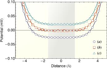
The model of all-around gated nanotube, inspired by the seminal paper of Luryi Luryi88 , can be simplified into an equivalent circuital model shown in Fig. 1(b). A modification beyond the original work is an addition external capacitance () in parallel to the main circuit. This external capacitance accounts for possible charge accumulations at the metallic planes outer to the nanotube. The capacitance accounts for the separating oxide insulator, while quantifies the accumulated charge at the metallic plates inner to the CNT. The induced charge on the surface of the nanotube leads to quantum capacitance, denoted by . The numerical values of as a function of carrier density can be straightforwardly obtained after establishing relations between electrostatic potential profiles and doping level . Fig. 2 shows three regimes of potential profiles along the direction (shown in Fig. 1) where the carrier densities are (a) , (b) , and (c) Å-1 respectively, and the applied gate voltage is mV. Explanations of these potential regimes in relations to carrier densities are detailed in the caption. The nanotube either (a) overscreens, (b) completely screens, or (c) partially screens the gate potential depending on the carrier densities Giuliani05 . This screening behavior of the nanotube are largely caused by the exchange energy function (through varying carrier densities).
The preceding paragraphs and the accompanying figures make it clear that the rather specific geometric setup of the nanotube, insulator, metallic gate and planes allows for direct calculations of . Taking advantage of the three screening regimes and the circuit model shown in Fig. 1(b), the quantum capacitance is obtained by computing the number of induced charge as a function of the carrier densities. By numerically evaluating the charged induced on the metallic planes shown in Fig. 1 (a), we find that both and for all current long CNTs studied are negligible. The gate capacitance in the circuit model in Fig. 1(b) hence reduces to . In the case of complete screening, we have whereas, for partial screening or over screening . Since the gate voltage is externally controlled, in both cases can be equated to yield the quantum capacitance as
| (3) |
where is a critical value of the carrier densities when complete screening is observed. The task of computing quantum capacitance then reduces to determining , and the induced charge at each doping levels. Here, an additional numerical optimizing routine has been implemented in coordination with the DFTB+NEGF package Aradi07 ; Pecchia04 ; DiCarlo05 in order to obtain the induced charge. This numerical routine appropriately sets Fermi levels, necessary for integrating the energy subbands for charge densities. A necessary condition to determine the Fermi levels is the charge neutrality. The charge tolerance in the Fermi energy optimizing routine is set to a.u. After obtaining appropriate Fermi energies, the NEGF routine is then utilized to draw electrons from source and drain onto the cylindrical surface of the nanotube Pecchia04 ; DiCarlo05 .
Small uniaxial stretch and compression can be applied the nanotube using the relation . Quantum capacitances at three strain levels are shown in Fig. 3. As well-evident from the figure, for an appropriate doping level, can change both its sign and magnitude depending upon the level of applied mechanical strain. For example at the carrier density of about 0.10 Å-1, changes from very high positive value at the % to about aF at %. For the (10,0) nanotube considered, this change in amounts for about % change in the overall capacitance in the classical complete screening case. Computed from from expressions leading Eq.(3), the classical capacitance is aF. The change in sign at the carrier density Å-1 can be interpreted as follows.
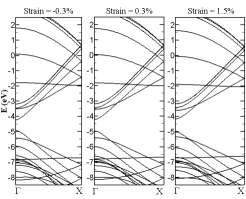
As the level of strains goes from small compression to tensile, the electronic density decreases due to an increase in the cylindrical tube area. At a sufficiently low electron density, the exchange contribution dominates the kinetic part to the capacitance. The exchange energy alone overwhelms and produces a negative quantum capacitance. By examining the band diagrams of the electronic ground state of the nanotube in Fig. 4 at different strain levels, it is clear that densities of states are not altered much across the range of strain considered. The kinetic contribution, which manifests through the density of states Kopp09 , thus plays a less crucial role in tuning magnitude and sign of in the nanotube under study.
In summary, we have explored the notion of switching the sign of quantum capacitance via mechanical strain, using a coaxially gated carbon nanotube as a model material system. From full electronic structure calculations within density functional tight-binding theory, it is clear that the interplay between doping and exchange energy functional play crucial roles in determining both the sign and magnitude of quantum capacitance. Fig. 3 clearly demonstrates that the quantum capacitance can be mechanically controlled from very large positive to very large negative values. It is then natural to ask if this nanotube property can be utilized in nanosensing technology. We envision that one possible technique to detect such a large negative/positive quantum capacitance is to modify the ingenious apparatus in Eisenstein92 . A pair of graphene could be used as place holders for 2DEG. The graphene could be set on piezoelectric materials to simulate strains, while small gates can be intentionally attached to add/remove electrons to the system. Strong signals of ratio between differential change in gate electric field and the penetrating fields ought to be observed. As discussed in Eisenstein92 , the ratio correlates directly to quantum capacitance. It should be emphasized that the concept of quantum capacitance is not only limited to CNT. Exploring the mechanical effects in other material systems such as BN monolayers, LaAlO3/SrTiO3 films could very well open new possibility in improving lower-power devices, and in energy storage for nanoelectronics. Moreover, the switching of sign promises a novel “quantum sensing” mechanism.
Acknowledgements.
YH and XL acknowledge useful correspondences with Alessandro Pecchia, Aldo Di Carlo, Bálint Aradi and Gabriele Penazzi during the course of this work.References
- (1) M. Büttiker. J. Phys. : Condens. Matter., 5:9361, 1993.
- (2) M. Stengel and N. A. Spaldin. Nature, 443:679, 2006.
- (3) M. Stengel, D. Vanderbilt, and N. A. Spaldin. Nature, 8:392, 2009.
- (4) C. A. Mead. Phys. Rev. Lett., 6(10):545, 1961.
- (5) M. M. Saad, P. Baxter, R. M. Bowman, J. M. Gregg, F. D. Morrison, and J. F. Scott. J. Phys. : Condens. Matter., 16:L451, 2004.
- (6) D. S. Boesch, J. Son, J. M. LeBeau, J. Cagnon, and S. Stemmer. Appl. Phys. Exp., 1:091602, 2008.
- (7) T. Kopp and J. Mannhart. J. Appl. Phys., 106:064504, 2009.
- (8) S. Luryi. Appl. Phys. Lett., 52:501, 1988.
- (9) S. Ilani, L. A. K. Donev, M. Kindermann, and P. L. McEuen. Nature Physics, 2:687, 2006.
- (10) L. Li, C. Richter, S. Paetel, T. Kopp, J. Mannhart, and R. C. Ashoori. Science, 332:825, 2011.
- (11) Z. Liu, Y. Zhan, G. Shi, S. Moldovan, M. Gharbi, L. Song, L. Ma, W. Gao, J. Huang, R. Vajtai, F. Banhart, P. Sharma, J. Lou, and P. M. Ajayan. Nature Communications, 3:1, 2012.
- (12) G. L. Yu, R. Jalil, B. Belle, A. S. Mayorov, P. Blake, F. Schedin, S. V. Morozov, L. A. Ponomarenko, F. Chiappini, S. Wiedmann, Uli Zeitler, M. I. Katsnelson, A. K. Geim, K. S. Novoselov, and D. C. Elias. PNAS, 110:3282, 2013.
- (13) G. F. Giuliani and G. Vignale. Quantum Theory of the Electron Liquid. Cambridge University Press, Cambridge, 2005.
- (14) M. M. Fogler. Phys. Rev. Lett., 94:056405, 2005.
- (15) S. K. Kusminskiy, J. Nilsson, D. K. Campbell, and A. H. Castro Neto. Phys. Rev. Lett., 100:106805, 2008.
- (16) G. Borghi, M. Polini, R. Asgari, and A. H. MacDonald. Phys. Rev. B, 82:155403, 2010.
- (17) B. Aradi, B. Hourahine, and Th. Frauenheim. J. Phys. Chem. A, 111:5678, 2007.
- (18) A. Pecchia and A. Di Carlo. Reports on Progress in Physics, 67:1497, 2004.
- (19) A. Di Carlo, A. Pecchia, L. Latessa, Th. Frauenheim, and G. Seifert. Introducing Molecular Electronics, chapter Tight-Binding DFT for Molecular Electronics (gDFTB), page 153. Springer, 2005.
- (20) L. Latessa, A. Pecchia, and A. Di Carlo. Phys. Rev. B, 72:035455, 2005.
- (21) E. Rauls, R. Gutierrez, J. Elsner, and Th. Frauenheim. Sol. State. Comm., 111:459, 1999.
- (22) L. Latessa, A. Pecchia, and Aldo Di Carlo. IEEE Transactions on Nanotechnology, 6(1):13–21, 2007.
- (23) J. P. Eisenstein, L. N. Pfeiffer, and K. W. West. Phys. Rev. Lett., 68(5):674, 1992.