Development of a Diehard GEM using PTFE insulator substrate
Abstract
We have developed the gas electron multiplier (GEM) using polytetrafluoroethylene (PTFE) insulator substrate (PTFE-GEM). Carbonization on insulator layer by discharges shorts the GEM electrodes, causing permanent breakdown. Since PTFE is hard to be carbonized against arc discharges, PTFE-GEM is expected to be robust against breakdown. Gains as high as 2.6104 were achieved with PTFE-GEM (50 m thick) in Ar/CO2 = 70/30 gas mixture at VGEM= 730 V. PTFE-GEM never showed a permanent breakdown even after suffering more than 40000 times discharges during the experiment. The result demonstrates that PTFE-GEM is really robust against discharges. We conclude that PTFE is an excellent insulator material for the GEM productions.
keywords:
GEM; Gas electron multiplier; PTFE-GEM; Arc resistance; Laser micro-fabrication; Femtosecond laser1 Introduction
The gas electron multipliers (GEMs), which have been developed at CERN by F. Sauli [1], are one of the micro-pattern gas detectors that detect X-rays and charged particles with good spatial resolution. We can easily manufacture a large size GEM detector with lower cost than the same size of semiconductor detector, and we can obtain better position resolution with GEM than with a scintillator detector. Thus, GEMs have been used in many fields, such as particle and nuclear physics, radiology, non-destructive testing and so on.
For the “standard GEM”, 50 m thick copper coated Kapton substrate is used. Typically, a number of through-holes with a diameter of 70 m are etched with a pitch of 140 m into the substrate [1]. We also uses a CO2 laser etching technique for drilling the copper cladded polyimide (PI-GEM) [2] or liquid-crystal polymer (LCP-GEM) [3].
High potential differences, which is necessary to achieve high gains, can cause permanent damage by electric discharge. To handle this problem, a statistical model predicting the GEM survival probability to discharge events is proposed by Cardini et al. [4]. On the other hand, the resistive electrode GEM (RE-GEM) and Thick-GEMs were proposed and studied to reduce a chance of breakdown by the electric discharge [5, 6]. We consider a solution to this problem the usage of new dielectrics as insulator for a GEM. Here we will present our results of a new GEM using polytetrafluoroethylene (PTFE) as insulator.
2 The choice of an insulator material
2.1 Observation of a damaged standard GEM
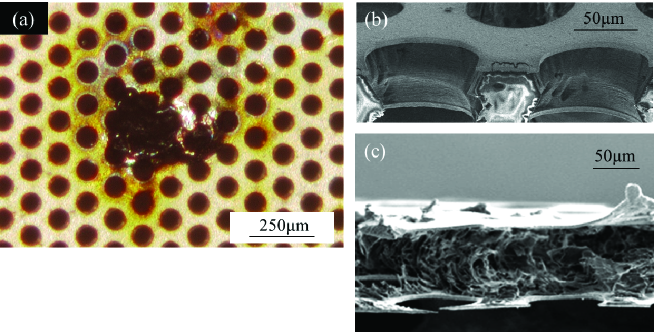
To investigate a primary risk to the GEM foil in operations, we have analyzed a damaged GEM foil. Figure 1(a) shows a top view of the PI-GEM damaged by abnormal discharges. The surface was carbonized and the copper foil peeled off. Figure 1(b) shows a scanning electron microscopic (SEM) image at the cross-section of the normal part of the PI-GEM which was cut by an ultra-microtome. We have demonstrated that the ultra-microtome technique was most suitable method for obtaining the cross-section of the GEM foil [7]. Figure 1(c) shows a SEM image at the cross-section of the damaged part. From those SEM images, we conclude that the insulating layer changed into a porous body. Moreover, the charging-up on the surface of the sample was not observed during the SEM imaging, which normally occurs when the sample has a large surface resistivity. Therefore we conclude that the resistivity around the burned section was reduced due to carbonization of polymer.
Kapton, the standard insulator for GEMs, has the advantage of being a commercial mass product and is widely used for the production of flexible circuit boards. However, it has the disadvantage that it easily carbonizes under the influence of the arc discharges during operations. Thus, we thought that the robustness of the GEM may improve if we can find a good insulating material which is not carbonized by electrical discharges.
2.2 Arc resistance test
To find a new material for the GEM insulator, we surveyed many polymers and evaluated four of them by using an arc resistance test method. The arc resistance is the ability of a material to resist the influence of arc discharge. In the method, the arc resistance is defined as the duration in seconds where the material resists the formation of a surface-conducting path when subjected to an intermittently occurring arc discharge of high voltage at a low current characteristics [8]. The thickness of a specimen in the test was 3 mm by definition. Although the thermal conduction might be quite different for thin foils, these tests is useful for comparing different materials. Failure of the specimen may be caused by heating to incandescence, burning, tracking or carbonization of the surface.
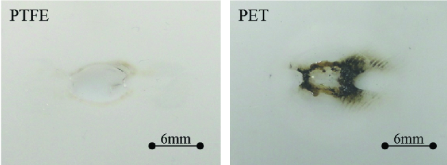
The characteristics of some well-known plastics, PI, LCP, polyethylene terephthalate (PET), and PTFE are summarized in Table 1. Among all the materials, PTFE has the highest value of the arc resistance. We have evaluated the arc resistance with the test equipment HAT-100 (a production of Hitachi Chemical Company, Ltd.) for PTFE and PET. The test results are shown in figure 2. The part of PET exposed by arc discharges was melted and burned, and a dip like a crater was formed. The similar dip was seen on the surface of PTFE, but there was no burnt deposit. To improve the lifetime of the GEM foil against discharges, PTFE has the potential to be a suitable material as insulating layer.
| materials | PI | LCP | PET | PTFE |
| Density (g/cm2) | 1.43 | 1.35 | 1.4 | 2.13-2.20 |
| Tension strength (MPa) | 315 | 108 | 48-73 | 20-35 |
| Water absorption () | 1.3 | 0.08 | 0.4 | 0 |
| Volume resistivity (cm) | 1017 | 61016 | 1017 | 1018 |
| Arc resistance (s) | 135 | 186 | 117 | 300 |
| Melting point (deg C) | - | - | 258 | 327 |
3 Production of PTFE-GEM
3.1 Metal deposition on PTFE
Since we could not find an appropriate commercial PTFE substrate which was laminated with copper foils without any adhesive, we fabricated the PTFE film with copper electrodes by ourselves. Copper was sputtered on both sides of the 50 m thick PTFE film, whose thickness was selected because the standard CERN GEM uses the 50 m thick PI, by the magnetron sputtering system SX-200 (ULVAC, Inc.). The sputtering conditions were as follows: 1 kW of the applied DC power, 0.67 Pa of the pressure, 120 mm of the length between the target and the sample, 10 rpm for the rotation speed, and 22 min of sputtering time. The sputtering was performed intermittently so that the PTFE did not thermally transform by heat. The thickness of the copper layer deposited on the PTFE film was 1.0 0.2 m measured with a stylus profiler Dektak150 from Veeco Instruments Inc.
3.2 Laser drilling through the PTFE substrate
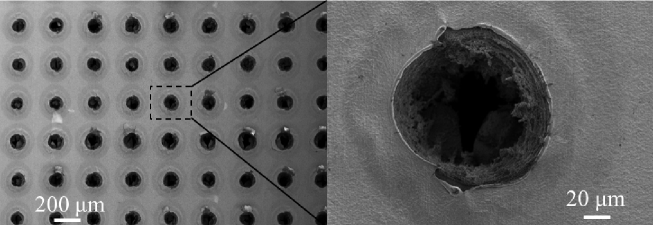
Methods such as chemical, plasma, and laser etching techniques are used for drilling holes through the substrate of the GEM foil production. Since PTFE has strong chemical resistance, the chemical etching was hard to realize. First, we tried to drill the holes through the copper-sputtered PTFE film using a CO2 laser. Figure 3 shows a photo of the substrate drilled with a 30 W of CO2 laser. Since many debris remained inside the through-holes and thermal damage by the laser could not be avoided, we gave up to use the CO2 laser for this purpose. In addition, the diameter of holes became more than 100 m (we expected around 70 m.) and the diameter was not controllable by our current method.
Afterwards, we tried to drill the through-holes using a femtosecond laser. By using this type of laser we can avoid heating-up the substrate during the process. In addition, the multi-photon absorption occurs under the extreme condition of the femtosecond laser, resulting the efficient drilling as if an ultra-violet laser. The mean wavelength of our femtosecond laser was 780 nm and the oscillation frequency was 1 kHz. The laser beam was scanned by a galvano scanner, and was focused on the surface of a sample with a telecentric lens of 100 mm focal length.
The copper-sputtered PTFE substrate we explained in the previous section was used. The processing conditions were as follows: an output power of 170 mW, a scanning speed of 0.5 mm/s, the pitch of zig-zag arrangement of 200 m, and a processing area of 2020 mm2. When we drilled a hole, we moved the focal point of the laser so that it created a circle with a diameter of 10 m around the center of the hole. Figure 4 shows the SEM images of upper (irradiated side by the laser) and lower surfaces of the PTFE substrate.
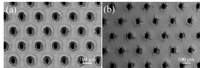
The shape of the through-holes was conical where the diameters of the upper and lower sides were about 80 and 30 m, respectively. Since the beam spot of the femtosecond laser was not true-circle, the shape of the holes became somewhat oval. In addition, the sputtered copper was removed around the edge of the through-holes in both upper and lower sides, and cracks on the copper were also seen. Those defects are probably caused by the weakness of the film adhesion between copper and PTFE, and the higher absorption rate of laser power in copper than in PTFE.
The production quality of the PTFE-GEM foils inspected by eyes was not good as we expected. However, we tested them if they work properly as GEM because the resistance between the electrodes was more than 20 T, which was quite enough for operation. We left the improvement on the production of the PTFE substrate and on the etching methods for future works.
4 Evaluation of PTFE-GEM
4.1 Experimental setup
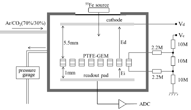
Figure 5 shows a schematic view of the GEM test setup used in this study. The setup consisted of a cathode, a PTFE-GEM foil, and a readout pad. PTFE-GEM was 50 m thick with an active area of 20 20 mm2 explained in §3. The cathode was a 15 m thick aluminum foil. The cathode, PTFE-GEM, and readout pad were placed in a chamber which was then filled with gas. The vertical space of the target region, which was the space between the cathode and PTFE-GEM, was 5.5 mm, and the induction region between PTFE-GEM and the readout pad was 1.0 mm. A high voltage was applied via a chain of 10 M resistors. To minimize the risk of electric surges, a 2.2 M protection resistor was added in the series with each GEM electrode. The electric field in the drift region was = 2.5 kV cm-1 and inside of the induction region was = 4-5 kV cm-1. During the test, Ar/CO2=(70%/30%) gas was made to flow through the system. Charge signals from the readout pads were fed into an amplifier, then the signals were digitized by an VME-ADC module.
4.2 Gain curves
The effective gain () of PTFE-GEM is given by
| (1) |
is the ADC peak value of incident monochromatic X-rays, is the electron charge (1.602 10-19 C), and is the number of electron-ion pairs created by an X-ray photon. A typical value of ne is 212 for a 5.9 keV X-ray photon from the radioactive 55Fe source in the Ar/CO2=(70%/30%) gas mixture [9]. The constant value is derived from a calibration curve obtained with a test pulse.
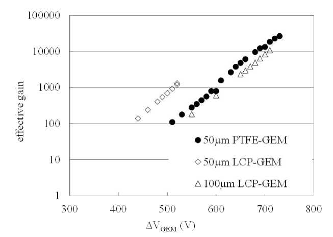
Figure 6 shows the gain curve of 50 m thick PTFE-GEM. The effective gain of PTFE-GEM we achieved was about 2.6104 at the applied voltage between PTFE-GEM electrodes of 730 V. We stopped the gain curve measurement at this voltage because of the limitation of the amplifier dynamic range. The gain curves for 50 m thick LCP-GEM and 100 m thick LCP-GEM are superposed in the same figure for comparison. The gradient of 50 m thick PTFE-GEM was similar to that of 50 m or 100 m thick LCP-GEM. The normalization of 50 m thick PTFE-GEM was almost the same as that of 100 m thick LCP-GEM. Since the copper electrode receded from the through-hole edge as shown in figure 4, the amplification region affected by the path length and the electric field strength might be different from the 50 m thick LCP-GEM.
4.3 Robustness against discharges
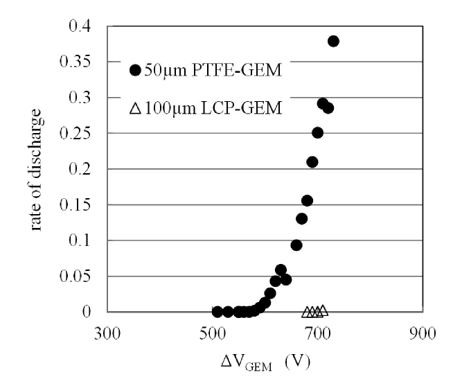
Figure 7 shows the rate of discharges of PTFE-GEM as a function of applied voltage between the GEM electrodes. For comparison, the discharge rate of the 100 m thick LCP-GEM is superposed in the same figure. The discharge rate of PTFE-GEM was higher than that of LCP-GEM. This is probably due to the rough structure around the edge of the through-holes (See figure 4.). The roughness of the hole edge should be improved in the next PTFE-GEM production.
The most important feature of PTFE-GEM against discharges is that it never showed a permanent damage during the experiment. (The cumulative number of discharges exceeded 4104 times.) On the other hand, the LCP-GEM suffered permanent breakdown after 91 discharges at an applied voltage of 710 V. We were convinced that the PTFE-GEM is really robust against discharges. We would like to stress that we are not suggesting to operate PTFE-GEM under continuous discharges, this should be avoided for this kind of GEM as also for the standard GEM, but we demonstrated that the PTFE is very robust against discharges.
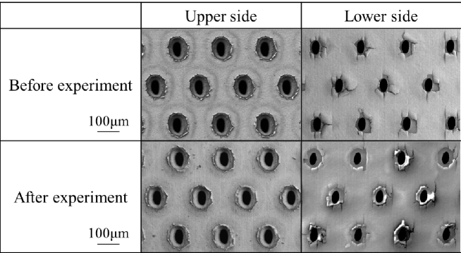
After the experiment, we have inspected the effective area of PTFE-GEM with SEM. In figure 8 the SEM images of PTFE-GEM for before and after the experiment are shown. Across the entire region of PTFE-GEM no carbonization, melting, or porous body was observed. As conclusion of our experiment, PTFE-GEM has superior characteristic that was not affected by discharges and PTFE is one of the best insulator materials for GEMs due to this fact although further work is necessary to optimize the production process.
5 Summary and Outlook
We have searched the insulator material which is hard to carbonize when it is exposed by discharges. Judging from the arc resistant tests, we selected PTFE as an insulator material for our GEM foil production. We have produced the PTFE-GEM foils for the first time: we formed copper electrodes on both sides of the PTFE film by magnetron sputtering, and then drilled through-holes by using a femtosecond laser processing technique.
We have measured the effective gain of PTFE-GEM. The gain we achieved was about 2.6104 for the 50 m thick PTFE-GEM in Ar/CO2=(70%/30%) gas mixture at an applied voltage of 730 V between the PTFE-GEM electrodes. The gain curve was similar to that of the 100 m thick LCP-GEM. The discharge rate of PTFE-GEM was quite high probably because of the roughness of the edges around the through-holes. However, PTFE-GEM was never destroyed despite of the fact that it suffered more than 40 thousand discharges during the experiment. We have experimentally confirmed that PTFE-GEM is really robust against discharges. No defect was observed on the PTFE-GEM surface with SEM after the experiment.
As conclusion of our experiment, PTFE-GEM has superior characteristic that was not affected by discharges. PTFE is one of the best insulator materials for the GEM production although further work is necessary to optimize the production process. To improve the production process, we are fabricating the PTFE substrate with thicker foil electrodes, since the thicker electrode can minimize the damage by heat in drilling the holes. Another possible improvement is to use an UV laser for drilling the PTFE substrate. A high energy laser may be easily punch the substrate without heat damage.
We have an outlook to use PTFE-GEM for space applications such as photoelectron tracking X-ray polarimeters [10, 11]. The polarimeters are basically a coupling of single layer GEM to a fine pixel readout chip. Using a stack of GEMs introduces an additional smearing which limits the imaging capability of the system, while one needs high gains at the same time. To achieve a good imaging performance, the robustness of PTFE-GEM against discharges is crucial.
Acknowledgements.
We thank Dr. K. Sunouchi and Dr. I. Takahashi at RIKEN for their help to use the femtosecond laser. We thank Dr. K. Fujiwara and Mr. T. Kobayashi at Tokyo Metropolitan Industrial Technology Research Institute (TIRI) for their discussions and comments. This work was partially supported by JSPS KAKENHI Grant Number 22244034.References
- [1] F. Sauli, Nucl. Instr. and Meth., A386, (1997) 531.
- [2] T. Tamagawa, et al., Nucl. Instr. and Meth., A560, (2006) 418.
- [3] T. Tamagawa, et al., Nucl. Instr. and Meth., A608, (2009) 390.
- [4] A. Cardini, et al., IEEE Nuclear Science Symposium Conference Record, (2005) 1127-1131.
- [5] A. Yoshikawa, et al., Journal of Instrumentation., Vol.7, Issue06, (2012) C06006.
- [6] A.Breskin, et al., Nucl. Instr. and Meth., A598, (2009) 107.
- [7] K. Komiya, et al., RIKEN Accelerator Progress Report, 45, (2012) 170.
- [8] ASTM Stand., (2004) D495-99.
- [9] F. Sauri, CERN Yellow Report, (1997) 77-09.
- [10] R. Bellazzini, et al., Nucl. Instr. and Meth., A560, (2006) 425.
- [11] J.K. Black, et al., Nucl. Instr. and Meth., A581, (2007) 755.