Spontaneous breaking of time reversal symmetry in strongly interacting two dimensional electron layers in silicon and germanium
Abstract
We report experimental evidence of a remarkable spontaneous time reversal symmetry breaking in two dimensional electron systems formed by atomically confined doping of phosphorus (P) atoms inside bulk crystalline silicon (Si) and germanium (Ge). Weak localization corrections to the conductivity and the universal conductance fluctuations were both found to decrease rapidly with decreasing doping in the Si:P and Ge:P layers, suggesting an effect driven by Coulomb interactions. In-plane magnetotransport measurements indicate the presence of intrinsic local spin fluctuations at low doping, providing a microscopic mechanism for spontaneous lifting of the time reversal symmetry. Our experiments suggest the emergence of a new many-body quantum state when two dimensional electrons are confined to narrow half-filled impurity bands.
Invariance to time reversal is among the most fundamental and robust symmetries of nonmagnetic quantum systems. Its violation often leads to new and exotic phenomena, particularly in two dimensions (2D), such as the quantized Hall conductance in semiconductor heterostructures Klitzing et al. (1980), the quantum anomalous Hall effect in topological insulators Chang et al. (2013) or the predicted chiral superconductivity in graphene Nandkishore et al. (2012). The breaking of time reversal invariance is experimentally achieved either by an external magnetic field or intentional magnetic doping. Here we show that strong Coulomb interactions can also lift the time reversal symmetry in nonmagnetic 2D systems at zero magnetic field.
While bulk P-doped Si and Ge have been extensively studied in the context of electron localization in three dimensions Rosenbaum et al. (1983); Dai et al. (1992); Lakner and Löhneysen (1989a); Paalanen et al. (1988); Sachdev (1989); Milovanović et al. (1989), confining the dopants to one or few atomic planes (layers) of the host semiconductor has recently led to a new class of 2D electron system Goh et al. (2006); Scappucci et al. (2012); Weber et al. (2012); Fuechsle et al. (2012). Electron transport in these atomically confined 2D layers occurs within a 2D impurity band where the effective Coulomb interaction is parameterized in terms of , with being the Coulomb energy required to add an additional electron to a dopant site, and , the hopping integral between adjacent dopants. Since each dopant P atom contributes one valence electron, the impurity band is intrinsically ’half filled’ (schematic in Fig. 1a), which reinforces the interaction effects due to the in-built electron-hole symmetry, and forms an ideal platform to explore the rich phenomenology of the 2D Mott-Hubbard model, ranging from Mott metal-insulator transition (MIT) to novel spin excitations and magnetic ordering Byczuk et al. (2005); Denteneer et al. (1999); Kohno (2012); Nielsen and Bhatt (2007).
In this Letter we show evidence of spontaneously broken time reversal symmetry in 2D Si:P and Ge:P -layers as the on-site effective Coulomb interaction is increased by decreasing the doping density of P atoms. Quantum transport and noise experiments indicate a strong suppression of quantum interference effects at low doping densities. We could attribute this to a spontaneous breaking of time reversal symmetry which manifest in an unambiguous suppression of universal conductance fluctuations (UCF) at zero magnetic field.
The preparation of the P -layers in Si and Ge have been detailed in earlier publications Goh et al. (2006); Goh (2006); Scappucci et al. (2012), and parameters relevant to the present work is supplied in the Supplementary Information (SI). The Drude conductivity () of the -layers decreases with decreasing doping as (Fig. 1b), where is the electron density measured from Hall effect, implying significant scattering from charged dopants Hwang and Das Sarma (2013). We find in all devices, ensuring a nominally weakly localized regime. All electrical transport measurements were carried out in a dilution refrigerator with an electron temperature of K using low frequency ac lock-in technique. The electron transport was strictly diffusive with , because of short momentum relaxation times fs, and displays negative logarithmic correction to conductivity in the quantum coherent regime (Fig. 1c) Scappucci et al. (2012).
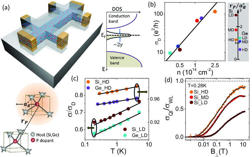
The key advantage of using both Si and Ge as host semiconductors is the factor of three difference in the Bohr radius, , which allows us to achieve a wide range of average effective dopant separation () within the similar range of doping density (). As shown in the scale bar of Fig. 1b, has an overall range from to 3. This corresponds to a range of meV and meV for the Ge:P and Si:P devices respectively, assuming hydrogenic orbitals Shklovskii and Efros (Springer-Verlag, Berlin Heidelberg New York Tokyo, 1984). Since meV and meV for single P donor in Si and Ge, respectively, the effective on-cite Coulomb interaction can be , particularly in lightly doped Si devices.
In Fig. 1d, we show the transverse magnetic field () dependence of the quantum correction to conductivity, , where , is the classical correction to the Drude conductivity. Due to diffusive nature of our devices the quantum correction from the electron-electron interaction is only perturbative ( , where is the cyclotron frequency) Gornyi and Mirlin (2003) and represents the contribution primarily from the quantum interference effect. for three 2D Si:P -layers at K is shown in Fig. 1d. For comparison, is scaled by , where is the universal weak localization correction to conductivity for a diffusive 2D conductor with free electrons. For each device, both and the phase breaking field (shown by vertical lines in Fig. 1d) were experimentally estimated from the low- magnetoconductivity data (see SI, section S3), where and are the phase coherence time and electron diffusivity, respectively. Since the magnitude of at represents the net correction to conductivity due to quantum interference, it is evident from Fig. 1d that the contribution of weak localization effect on transport decreases with decreasing doping density (see SI, section S1). It is important to note that a major shift in the dominant dephasing mechanism in the lightly doped samples is ruled out because we find to be similar in magnitude in all three devices, and down to K (Fig. S2 in SI). This confirms the predominance of the electron-electron scattering mediated dephasing which has been reported earlier in such -layers Scappucci et al. (2012).
The reduced quantum correction cannot be due to finite experimental range ( T) of , which exceeds both and (, the upper cutoff field due to momentum relaxation) by factors of and respectively even for the least doped devices at K (Table I in SI). Spin-orbit interaction is also known to be small for P-doped (bulk) Si and Ge Ghosh and Raychaudhuri (2000); Dai et al. (1993), and independent of the density of the dopants. Any long range magnetic order is also unlikely because the Hall resistance was found to vary linearly with at all (see SI, section S7) in all our devices Nielsen and Bhatt (2007).
The suppression of quantum correction to conductivity has been observed in low density electron gases in Si MOSFETs near the apparent MIT Rahimi et al. (2003) although its microscopic origin remains unclear with both temperature dependant screening of disorder and interaction driven spin fluctuations suggested as competing mechanisms. However, the formation of local magnetic moments in the presence of strong Coulomb interactions, is known to occur in three dimensional P-doped Si close to the MIT Paalanen et al. (1988); Sachdev (1989); Milovanović et al. (1989). These moments serve to remove the time reversal symmetry, suppressing the coherent back-scattering of electrons. In 2D, the possibility of localized spin excitations at the Mott transition has been suggested theoretically Kohno (2012); Imada et al. (1998), but without any experimental evidence so far.
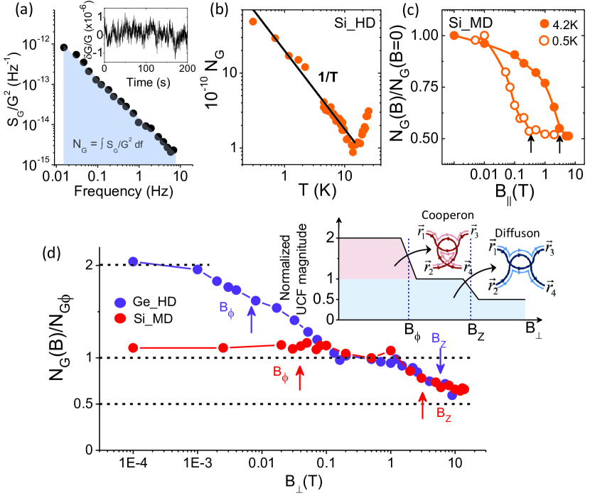
To probe whether the observed suppression of localization correction indeed manifests a breaking of the time reversal symmetry, we have measured the UCF as a function of and from slow time-dependent fluctuations in the conductance () of the -layers which represents the ensemble fluctuations via the ergodic hypothesis Stone (1989); Ghosh and Raychaudhuri (2000); Birge et al. (1990); McConville and Birge (1993); Feng et al. (1986). The time dependant conductance fluctuations (inset of Fig. 2a) are analyzed to obtain the power spectral density, , which on integration over the experimental bandwidth gives the normalized variance, as shown in Fig. 2a (see Ref Shamim et al. (2011) and SI, section S3 for details). Fig. 2b shows as a function of for Si_HD. For K, increases with decreasing , which is a hallmark of UCF. In this regime, one expects , where and are the phase coherence length and density of active two level fluctuators Birge et al. (1990) (Fig. 2b). The absolute magnitude of in all devices correspond to the change in conductance by due to a single fluctuator within a phase coherent box (see SI, section S5), establishing the observed noise to be indeed from mesoscopic fluctuations.
As a function of , the magnitude of UCF is expected to decrease by an exact factor of two at two field scales, first at when the time reversal symmetry, and hence the Cooperon (self-intersecting diffusion trajectories) contribution, is removed Altshuler and Spivak (1985); Stone (1989); Beenakker and van Houten (1991) and second at due to removal of spin degeneracy Stone (1989); Moon et al. (1996); Beenakker and van Houten (1991), where and are the -factor and respectively. The inset of Fig. 2d shows schematically the two reductions in UCF magnitude as a function of . Fig. 2d shows that the UCF magnitude in heavily doped Ge_HD (violet symbols) consists of both factors of two reduction at and , corresponding to the removal of time reversal symmetry and spin degeneracy, respectively, whereas the lightly doped devices, such as Si_MD, shows almost no variation in the UCF magnitude on the scale of but decreases by a factor of two at . To confirm this scenario, we have also recorded the variation of in Si_MD as a function of parallel magnetic field, , which couples only to spin degree of freedom (Fig. 2c). The factor of two reduction at (shown by vertical arrows in Fig. 2c) for K and K establishes that the noise in our devices indeed arises from the UCF mechanism.
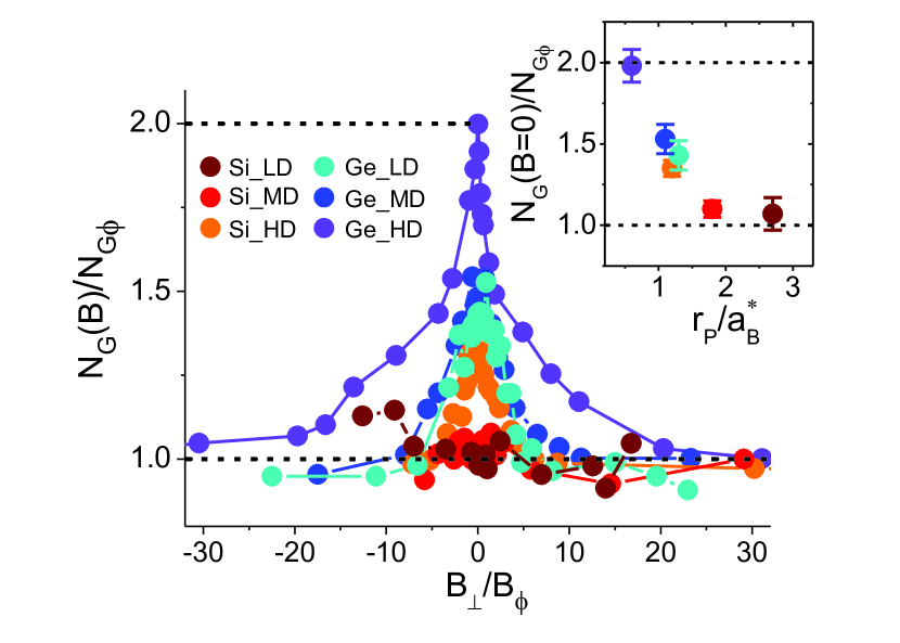
Since the reduction in UCF at is associated only to removal of the fundamental time reversal symmetry of the underlying Hamiltonian Altshuler and Spivak (1985), its absence in the lightly doped layers is unique, and has not been previously observed in interacting 2D systems in semiconductors Clarke et al. (2008); Abrahams et al. (2001). To elaborate, we have compiled the -dependence of normalized by , where is the value of at but , for all devices in Fig. 3. was chosen at which was for all the devices at all temperatures. The peak in around is progressively suppressed with decreasing doping density, and eventually for , the Cooperon contribution to UCF noise at low becomes immeasurably small, implying a spontaneous breaking of time reversal symmetry even at (Inset of Fig. 3).
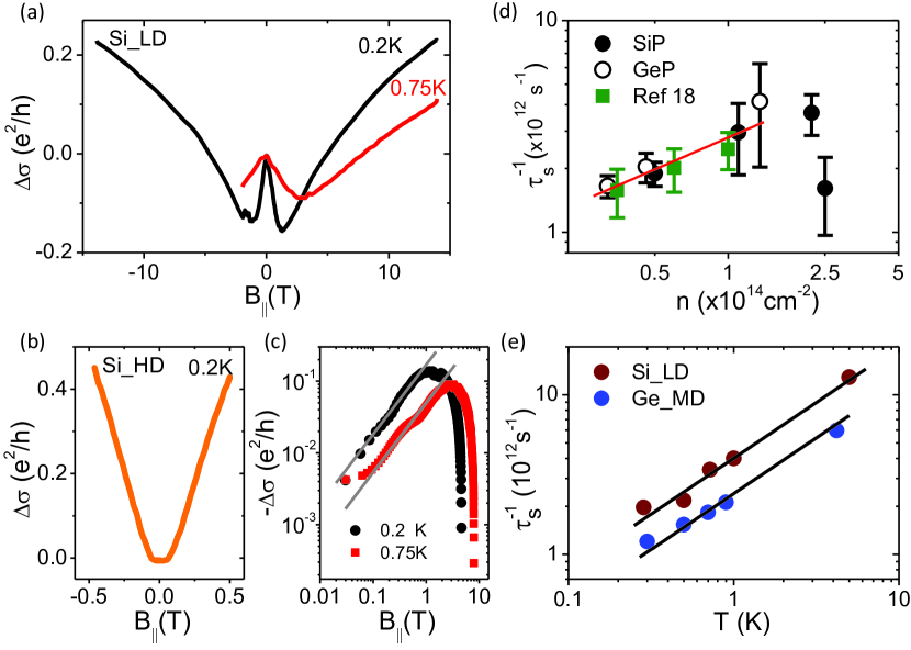
To explore the origin of lifting of the time reversal symmetry in the -layers, we subjected the devices to in-plane magnetic field, , that resulted in a nonmonotonic magnetoconductivity in the lightly doped -layers. The logarithmic increase in the magnetoconductivity at large , as shown in Fig. 4a, was observed in all devices irrespective of doping level, and known to represent suppression of weak localization due to the finite width of the -layers Meyer et al. (2002). However, the negative magnetoconductivity around often indicates the presence of local moments, because localization strengthens as phase coherence increases with the freezing of spin-flip scattering Christianson et al. (2002); Meyer et al. (2002). In such a case, the activated spin-flip processes across the Zeeman gap, leads to magnetoconductivity decreasing linearly with as , where , and is the -factor of the magnetic impurity Meyer et al. (2002). As shown in Fig. 4c, we indeed find the in Si_LD. The negative magnetoconductivity in is entirely absent in the heavily doped devices (Fig. 4b). This establishes that the spin fluctuations are entirely due to strong Coulomb interactions, and hence observable only in the lightly doped -layers. Importantly, the experimental value of was found to be a factor of smaller than that expected theoretically (assuming ), suggesting that the impact of local moments on the dephasing process is anomalously small.
The compelling analogy with the bulk P-doped Si close to MIT provides a “two-fluid” framework to address transport in our -layers. This consists of itinerant electrons in disordered Hamiltonian and local magnetic moments Paalanen et al. (1988); Sachdev (1989); Milovanović et al. (1989). The interaction between the local moments and itinerant electrons suppresses localization, although the spin-scattering process is quasi-elastic (energy exchange ), causing only minor modification to the dephasing mechanism (as confirmed by the linear dependence of in Fig. S2 of SI and small ). In addition, the two-fluid model allows a phenomenological generalized Hikami-Larkin-Nagaoka expression for the total quantum interference correction that includes the quasi-elastic spin scattering rate () as,
| (1) |
where and are positive constants close to unity, and , with being the digamma function. As shown by the solid lines in Fig. 1d, Eq. 1 describes the magnetoconductivity very well over the entire range of . The fit parameter , provides an estimate of the spin scattering time . We note the following: (i) As evident in Fig. 4d, is more than ten times larger than experimentally measured (see SI), confirming that the spin-scattering is mostly elastic. (ii) Second, varies nonmonotonically with . The filled squares represent analyzed from data of Ref Goh (2006). At low , irrespective of host material, disorder or carrier mobility, indicating that the number of local spins are only related with the number of P dopant sites. However drops abruptly around cm-2, suggesting a quenching of the spins and commencement of free-electron weakly localized quantum transport. The T-dependence of (Fig. 4e), in accordance with the two-fluid model, shows a power law variation as , with . This sets the exponent for susceptibilty and specific heat divergence in the -layers to be , which is about half of that observed in the bulk Si:P close to MIT Paalanen et al. (1988); Lakner and Löhneysen (1989b).
Finally, to estimate the fraction of P-dopants that host a local moment, we compare the estimated in lightly doped Si_LD ( cm-2) with (1) the total momentum relaxation rate s-1 from the experimental Drude conductivity, although this involves scattering from neutral defects as well, and (2) calculated momentum relaxation rate ( s-1) expected purely from the P-dopants (charged impurities) (see calculation details in Ref Hwang and Das Sarma (2013) and SI, section S6). This gives a bound between of the P-dopants to host local moments which is consistent with the fraction expected for half-filled impurity bands in bulk Si:P Milovanović et al. (1989). Importantly, while the weak localization correction is reduced only partially ( 30% in Si_LD), the UCF noise due to the Cooperons is completely suppressed for the weakly doped devices. It is possible that because the UCF noise involves interference between two Feynman propagators, it is more likely to be affected by the localized spins than the WL correction which is determined by a single self intersecting propagator. Note that we have not discussed spatial inhomogeneity or clustering in the distribution of dopants which can lead to coexistence of localized and delocalized phases Byczuk et al. (2005), impact of multiple valleys Punnoose and Finkel’stein (2005); Gunawan et al. (2006), or the inter-site Coulomb interaction Shepelyansky (1994); Clarke et al. (2008); Abrahams et al. (2001) which are unlikely to affect the time reversal symmetry.
In summary, magnetoconductivity and noise measurements reveal an unexpected spontaneous breaking of time reversal symmetry in 2D electron systems hosted in atomically confined Si:P and Ge:P crystals. The universal conductance fluctuations and in-plane magnetoconductivity suggest that local spin fluctuations in the presence of strong Coulomb interaction play an important role in the lifting the time reversal symmetry. Whether this indeed leads to a true interaction-induced metallic ground state in two dimensions needs further experimental and theoretical exploration.
I Acknowledgement
We acknowledge Sankar Das Sarma, Ravin N.Bhatt, Vijay Shenoy, Sanjoy Sarker and Jainendra Jain for discussions. We thank Department of Science and Technology (DST), Government of India and Australian-Indian Strategic Research Fund (AISRF) for funding the project. The research was undertaken in collaboration with the Australian Research Council, Centre of excellence for Quantum Computation and Communication Technology (Project number CE110001027) and the US Army Research Office under contract number W911NF-08-1-0527. SS thanks CSIR for financial support. GS acknowledges support from UNSW under the GOLDSTAR Award 2012 scheme. MYS acknowledges a Federation Fellowship.
References
- Klitzing et al. (1980) K. v. Klitzing, G. Dorda, and M. Pepper, Phys. Rev. Lett. 45, 494 (1980).
- Chang et al. (2013) C.-Z. Chang, J. Zhang, X. Feng, J. Shen, Z. Zhang, M. Guo, K. Li, Y. Ou, P. Wei, L.-L. Wang, et al., Science 340, 167 (2013).
- Nandkishore et al. (2012) R. Nandkishore, L. S. Levitov, and A. V. Chubukov, Nat. Phys. 8, 158 (2012).
- Rosenbaum et al. (1983) T. F. Rosenbaum, R. F. Milligan, M. A. Paalanen, G. A. Thomas, R. N. Bhatt, and W. Lin, Phys. Rev. B 27, 7509 (1983).
- Dai et al. (1992) P. Dai, Y. Zhang, and M. P. Sarachik, Phys. Rev. B 45, 3984 (1992).
- Lakner and Löhneysen (1989a) M. Lakner and H. v. Löhneysen, Phys. Rev. Lett. 63, 648 (1989a).
- Paalanen et al. (1988) M. A. Paalanen, J. E. Graebner, R. N. Bhatt, and S. Sachdev, Phys. Rev. Lett. 61, 597 (1988).
- Sachdev (1989) S. Sachdev, Phys. Rev. B 39, 5297 (1989).
- Milovanović et al. (1989) M. Milovanovi, S. Sachdev, and R. N. Bhatt, Phys. Rev. Lett. 63, 82 (1989).
- Goh et al. (2006) K. E. J. Goh, L. Oberbeck, M. Y. Simmons, A. R. Hamilton, and M. J. Butcher, Phys. Rev. B 73, 035401 (2006).
- Scappucci et al. (2012) G. Scappucci, W. M. Klesse, A. R. Hamilton, G. Capellini, D. L. Jaeger, M. R. Bischof, R. F. Reidy, B. P. Gorman, and M. Y. Simmons, Nano Letters 12, 4953 (2012).
- Weber et al. (2012) B. Weber, S. Mahapatra, H. Ryu, S. Lee, A. Fuhrer, T. C. G. Reusch, D. L. Thompson, W. C. T. Lee, G. Klimeck, L. C. L. Hollenberg, et al., Science 335, 64 (2012).
- Fuechsle et al. (2012) M. Fuechsle, J. A. Miwa, S. Mahapatra, H. Ryu, S. Lee, O. Warschkow, L. C. L. Hollenberg, G. Klimeck, and M. Y. Simmons, Nature Nanotechnology 7, 242 (2012).
- Byczuk et al. (2005) K. Byczuk, W. Hofstetter, and D. Vollhardt, Phys. Rev. Lett. 94, 056404 (2005).
- Denteneer et al. (1999) P. J. H. Denteneer, R. T. Scalettar, and N. Trivedi, Phys. Rev. Lett. 83, 4610 (1999).
- Kohno (2012) M. Kohno, Phys. Rev. Lett. 108, 076401 (2012).
- Nielsen and Bhatt (2007) E. Nielsen and R. N. Bhatt, Phys. Rev. B 76, 161202 (2007).
- Goh (2006) K. E. J. Goh, PhD Thesis, University of New South Wales (2006).
- Hwang and Das Sarma (2013) E. H. Hwang and S. Das Sarma, Phys. Rev. B 87, 125411 (2013).
- Shklovskii and Efros (Springer-Verlag, Berlin Heidelberg New York Tokyo, 1984) B. I. Shklovskii and A. L. Efros, Electronic properties of doped semiconductors (Springer-Verlag, Berlin Heidelberg New York Tokyo, 1984).
- Gornyi and Mirlin (2003) I. V. Gornyi and A. D. Mirlin, Phys. Rev. Lett. 90, 076801 (2003).
- Ghosh and Raychaudhuri (2000) A. Ghosh and A. K. Raychaudhuri, Phys. Rev. Lett. 84, 4681 (2000).
- Dai et al. (1993) P. Dai, Y. Zhang, S. Bogdanovich, and M. P. Sarachik, Phys. Rev. B 48, 4941 (1993).
- Rahimi et al. (2003) M. Rahimi, S. Anissimova, M. R. Sakr, S. V. Kravchenko, and T. M. Klapwijk, Phys. Rev. Lett. 91, 116402 (2003).
- Imada et al. (1998) M. Imada, A. Fujimori, and Y. Tokura, Rev. Mod. Phys. 70, 1039 (1998).
- Stone (1989) A. D. Stone, Phys. Rev. B 39, 10736 (1989).
- Birge et al. (1990) N. O. Birge, B. Golding, and W. H. Haemmerle, Phys. Rev. B 42, 2735 (1990).
- McConville and Birge (1993) P. McConville and N. O. Birge, Phys. Rev. B 47, 16667 (1993).
- Feng et al. (1986) S. Feng, P. A. Lee, and A. D. Stone, Phys. Rev. Lett. 56, 1960 (1986).
- Shamim et al. (2011) S. Shamim, S. Mahapatra, C. Polley, M. Y. Simmons, and A. Ghosh, Phys. Rev. B 83, 233304 (2011).
- Altshuler and Spivak (1985) B. L. Altshuler and B. Z. Spivak, Pis’ma Zh. Eksp. Teor. Fiz. 42, 363 (1985).
- Beenakker and van Houten (1991) C. Beenakker and H. van Houten, in Semiconductor Heterostructures and Nanostructures (Academic Press, 1991), vol. 44 of Solid State Physics, pp. 1 – 228.
- Moon et al. (1996) J. S. Moon, N. O. Birge, and B. Golding, Phys. Rev. B 53, R4193 (1996).
- Clarke et al. (2008) W. R. Clarke, C. E. Yasin, A. R. Hamilton, A. P. Micolich, M. Y. Simmons, K. Muraki, Y. Hirayama, M. Pepper, and D. A. Ritchie, Nat. Phys. 4, 55 (2008).
- Abrahams et al. (2001) E. Abrahams, S. V. Kravchenko, and M. P. Sarachik, Rev. Mod. Phys. 73, 251 (2001).
- Meyer et al. (2002) J. S. Meyer, V. I. Fal’ko, and B. L. Altshuler, eprint arXiv:cond-mat/0206024 (2002), eprint arXiv:cond-mat/0206024.
- Christianson et al. (2002) A. D. Christianson, A. H. Lacerda, M. F. Hundley, P. G. Pagliuso, and J. L. Sarrao, Phys. Rev. B 66, 054410 (2002).
- Lakner and Löhneysen (1989b) M. Lakner and H. v. Löhneysen, Phys. Rev. Lett. 63, 648 (1989b).
- Punnoose and Finkel’stein (2005) A. Punnoose and A. M. Finkel’stein, Science 310, 289 (2005).
- Gunawan et al. (2006) O. Gunawan, T. Gokmen, K. Vakili, M. Padmanabhan, E. P. De Poortere, and M. Shayegan, Nat. Phys. 3, 388 (2006).
- Shepelyansky (1994) D. L. Shepelyansky, Phys. Rev. Lett. 73, 2607 (1994).