One-dimensional Quantum Wire Formed at the Boundary Between Two Insulating LaAlO3/SrTiO3 Interfaces
Abstract
We grow a tiled structure of insulating two dimensional LaAlO3/SrTiO3 interfaces composed of alternating one and three LaAlO3 unit cells. The boundary between two tiles is conducting. At low temperatures this conductance exhibits quantized steps as a function of gate voltage indicative of a one dimensional channel. The step size of half the quantum of conductance is an evidence for absence of spin degeneracy.
pacs:
81.07.Vb,73.23.-b, 73.20.-rOxide interfaces can bring new functionalities into future electronic applications Mannhart and Schlom (2010). Of particular interest are oxide based quantum wires that have tuanble spin-orbit interaction and superconductivity Ben Shalom et al. (2010), making them an important ingredient in future spin-based electronic devices, and in revealing exotic states, such as Majorana fermions Oreg et al. (2010). The hallmark interface between LaAlO3 and SrTiO3 surprisingly exhibits properties of a two-dimensional (2D) electron gas Ohtomo and Hwang (2004), tunable superconductivity Caviglia et al. (2008), magnetism Bert et al. (2011); Li et al. (2011); Dikin et al. (2011); Brinkman et al. (2007); Wang et al. (2011) and tunable spin-orbit interaction Ben Shalom et al. (2010); Caviglia et al. (2010). Many attempts have been made to create a one dimensional (1D) channel out of the 2D LaAlOSrTiO3 interface, usually by narrowing down the 2D conductor using complex lithography techniques Rakhmilevitch et al. (2010). Here we present a new oxide 1D interface concept. This interface is formed between two 2D non-conducting interfaces of SrTiO3 and LaAlO3. We show that conducting electrons are confined to the boundary between these 2D interfaces in a potential well narrower than their Fermi wavelength. Consequently, they behave quantum-mechanically with their conductance appearing in discrete steps. From the step size we find that these electrons are spin polarized.
Epitaxial films of LaAlO3 are deposited using reflection high energy electron diffraction (RHEED) monitored pulsed laser deposition on atomically flat TiO2 terminated SrTiO3 substrate in standard conditions Ben Shalom et al. (2009). In order to obtain the structure illustrated in figure 1a we first deposit a single unit cell thick layer of LaAlO3, then using standard photo-lithography technique, the planar interface is defined by depositing an amorphous oxide layer ,at room temperature, parallel to the crystal axis. Schneider et al. (2006) followed by a liftoff step exposing the clean 1uc thick LaAlO3/SrTiO3 interface. Finally, a two unit cell thick layer of LaAlO3 is deposited. This results in a planar interface between 1uc thick LaAlO3/SrTiO3 interface with an amorphous capping layer and a 3uc thick LaAlO3/SrTiO3 interface. A gold layer is evaporated as a back-gate. Ti-Au contacts are evaporated after Ar ion milling of the contact area. These contacts probe a few parallel boundaries as described in figure1b. We use a wire bonder to connect voltage and current leads to each contact to eliminate the resistance of the leads, without eliminating the resistance between the metal and the planar interface. We ensured that the DC voltage drop across the sample was smaller than T ( being the Boltzmann constant and T is the temperature). The leakage current between the gate electrode and the device was always smaller than 1 nano-Ampere. Contact resistance is obtained by fitting the data to the Landauer formula with the contact resistance as a single fitting parameter
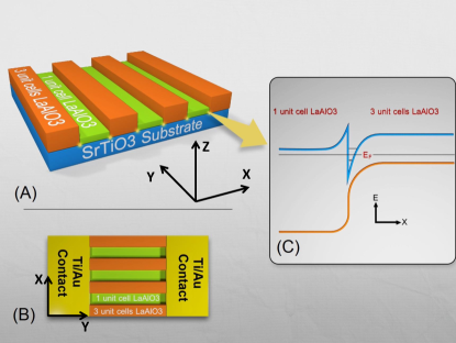
We verified that the layers themselves are insulating while the boundaries between them are conducting. No conductivity is expected neither at a 2D LaAlO3/SrTiO3 interface with a single nor with a triple unit cell thick LaAlO3 layer used in our devices since both layers are below the threshold for conductivity for the 2D SrTiO3/LaAlO3 interfaces Thiel et al. (2006). Furthermore, contacts that were put as close as 10m away from the planar interface showed no conductance, suggesting that the conductivity is confined to a very narrow region. The resistance between these contacts is unmeasurably high and so is the resistance between two adjacent devices. The unexpected conductivity at the planar interface must stem from its discontinuity (see Figure 1 a, b). Our results show that a potential well is formed along the y direction (see Figure 1a).
In Figure 2 the resistance as a function of temperature of one of these devices is shown. The overall behavior of the temperature dependence is similar to that observed in semiconductor heterojunctions Pfeiffer et al. (1989). The resistance increases upon cooling down, due to spurious carrier freeze-out. Further cooling results in a reduction of temperature-dependent scattering, such as electron-phonon. At low temperatures this process is overwhelmed by the depletion in the potential well formed. While the behavior described above is reproducible for each device, the details may vary from one sample to another. For example, the resistance extrema could appear at somewhat different temperatures for various devices. This may be related to random impurity states such as oxygen vacancies, La/Sr intermixing or other unknown impurity mechanisms.
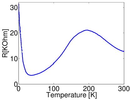
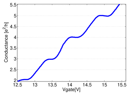
Figure 3 shows the conductance versus back-gate-voltage measured at 1.85 K for a long wire. Clear steps are observed. The step size is exactly half of the universal quantum conductance . This is indicative of the existence of a 1D confinement with quantized energy levels.
According to R. Landauer Imry (2002) the conductance in a 1D channel is quantized and can be expressed as
Here are the transmission coefficients of the various channels, and is the quantum conductance with the elementary charge and the Planck constant. For a ballistic device, whose length is shorter than the mean free path the transmissions, and
, where is an integer determined by the number of occupied modes.
The devices are comprised of a few parallel wires (figure 1b). Such parallel measurement can only increase the conductance relative to a single wire. If the population of two wires is increased within the same gate voltage range, the conductance will increase by a step twice as high as the usual one. (See supplementary materialSup for demonstration of such an occurrence).
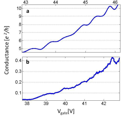
Conductance steps lower than can be observed when the transmission coefficients are smaller than unity, usually due to scattering along the wire Imry (2002). This is not the case in our device. To eliminate the low transmission coefficient scenario, we fabricate a shorter wire ( length) and a longer one (). It is expected that the scattering probability is increased with wire length. However, we observe a reproducible step height for both (see Figure 4a) and wires. A diffusive channel () is obtained only for the longer wire (see Figure 4b). This indicates a completely ballistic process for the shorter wires of up to . Furthermore, in the diffusive device, the step height is no longer uniform, as expected.
Another possible mechanism for conductance is the removal of spin degeneracy. This has been demonstrated to happen under applied magnetic field Quay et al. (2010). In the absence of an external magnetic field, this is possible if the conducting electrons are spin-polarized Ono et al. (1999); Wig .
Magnetic effects have been observed in the 2D interface between LaAlO3 and SrTiO3 using various probes Bert et al. (2011); Li et al. (2011); Dikin et al. (2011); Brinkman et al. (2007); Lee et al. (2013); Kalisky et al. (2012). This magnetism has been related to the polar nature of this interface Flekser et al. (2012) appearing only above a critical thickness of four unit cells Kalisky et al. (2012). It is therefore difficult to confirm whether the magnetic effects in 2D and the spin polarization reported here are of the same origin.
One may claim that the quantized conductance steps arise from a point contact connected in series to a 2D reservoir Van Wees et al. (1988). We rule out this possibility in our devices. A 2D conductor made of LaAlO3/SrTiO3 connected in series to a point contact would have a highly gate voltage-sensitive resistance. For example, for the gate voltage range studied here (see Figure 3 and supplementary materialSup ), one would expect the resistance of the presumed 2D section to change by a factor of 2.6 Ben Shalom et al. (2010). This would result in a noticeable deviation from the universal step values observed. We therefore conclude that our device is a quantum wire.
We now discuss possible mechanisms for the formation of the quantum wire at the 1D interface. While the origin of the 2D conductivity in the LaAlO3/SrTiO3 interface is still a matter of strong debate it has been established that conductivity appears only above a threshold of four LaAlO3 layers Thiel et al. (2006). A simplified electrostatic consideration suggests that adding LaAlO3 layers results in the accumulation of electrostatic potential energy. When this energy becomes of the order of the band gap of SrTiO3 conducting electrons are transferred into the interface.
A more detailed calculation showed that below the conductivity threshold Thiel et al. (2006) the gap between the unoccupied (titanium 3d states) and occupied bands (oxygen 2p states) monotonically decreases upon accumulation of LaAlO3 layers Pentcheva and Pickett (2006). Adopting this view the gap between the unoccupied and the occupied bands changes discontinuously across the 1D interface when the LaAlO3 layer thickness suddenly changes (say, along the x direction see fig1a). Consequently, a potential well should be formed (Figure 1c). Such discontinuity is similar to that implemented in semiconductor heterostructures with different band gaps (e.g. GaAs/AlxGa1-xAs). There, the band discontinuity is along the z axis resulting in a 2D potential well formed between the two semiconductors. Although in the semiconductor heterostructure charge modulation doping layer away from the interface is usually implanted in our case the origin of the initial charges is not clear to us. The fact that our interface is placed only 12 away from the surface and on top of SrTiO3 substrate, which has many doping mechanisms may explain the existence of charges as seen in the temperature dependence of our device.
It has been recently reported that the surface potential in LaAlO3/SrTiO3 interface has a stripe-like structure. These stripes are related to the domain structure of SrTiO3 below the cubic to tetragonal transition. Kalisky et al. (2013) It is possible that a domain wall is pinned to our planar interface resulting in a higher charge concentration and better mobility. However, this is not enough to explain the conductivity in the wire since for 3 unit cell thick LaAlO3 layer on top of SrTiO3 no conductivity is observed despite the domains. A detailed calculation taking into account the polar layers and the presence of domain wall is needed to explore this possibility.
The analysis of the conductance versus gate voltage in figures 3,4a yields a transmission coefficients very close to unity. i.e. the wires are ballistic. This is in spite of their lengths of 4 and 1 respectively. This is much longer than the mean free path of the order of , measured for the LaAlO3/SrTiO3 2D interface Ben Shalom et al. (2009).
Anomalous high mobility has recently been reported in SrTiO3/LaAlO3 nano-wires, defined using an atomic force microscope with a conducting tip Irvin et al. (2013). A mean free path enhancement in a 1D system, compared to a 2D case, is predicted due to a reduced phase space available for back-scattering Sakaki (1980). However, in semiconductors this enhancement is usually not large Kaufman et al. (1999). We conjecture that the long-ranged ballistic length in our case is a result of the polarized electrons experiencing spin-orbit interaction Ben Shalom et al. (2010); Caviglia et al. (2010). In such a scenario, backscattering is strongly suppressed, since reversing momentum direction requires spin-flip scattering and surmounting the exchange energy.
This letter presents a novel and simple method of fabricating a one-dimensional quantum wire, utilizing the polar structure of the LaAlO3/SrTiO3 interface. This new wire opens possibilities for long-ranged spin transport. Furthermore, the constituting oxides will introduce new functionalities and correlations into this wire Oreg et al. (2013). The possibility to control correlation effects, spin-orbit interactions and coupling to superconductivity makes this wire a laboratory for studying Majorana fermions Oreg et al. (2010) and fractional charges Oreg et al. (2013).
We thank Eran Sela, Alexander Palevski and Moshe Ben Shalom for useful discussions. This work was supported in part by the Israeli Science Foundation under grant no.569/13 by the Ministry of Science and Technology under contract 3-8667 and by the US-Israel bi-national science foundation (BSF).
References
- Mannhart and Schlom (2010) J. Mannhart and D. Schlom, Science 327, 1607 (2010).
- Ben Shalom et al. (2010) M. Ben Shalom, M. Sachs, D. Rakhmilevitch, A. Palevski, and Y. Dagan, Physical review letters 104, 126802 (2010).
- Oreg et al. (2010) Y. Oreg, G. Refael, and F. von Oppen, Physical review letters 105, 177002 (2010).
- Ohtomo and Hwang (2004) A. Ohtomo and H. Hwang, Nature 427, 423 (2004).
- Caviglia et al. (2008) A. Caviglia, S. Gariglio, N. Reyren, D. Jaccard, T. Schneider, M. Gabay, S. Thiel, G. Hammerl, J. Mannhart, and J.-M. Triscone, Nature 456, 624 (2008).
- Bert et al. (2011) J. A. Bert, B. Kalisky, C. Bell, M. Kim, Y. Hikita, H. Y. Hwang, and K. A. Moler, Nature physics 7, 767 (2011).
- Li et al. (2011) L. Li, C. Richter, J. Mannhart, and R. Ashoori, Nature Physics 7, 762 (2011).
- Dikin et al. (2011) D. Dikin, M. Mehta, C. Bark, C. Folkman, C. Eom, and V. Chandrasekhar, Physical Review Letters 107, 056802 (2011).
- Brinkman et al. (2007) A. Brinkman, M. Huijben, M. Van Zalk, J. Huijben, U. Zeitler, J. Maan, W. Van der Wiel, G. Rijnders, D. Blank, and H. Hilgenkamp, Nature materials 6, 493 (2007).
- Wang et al. (2011) X. Wang, G. Baskaran, Z. Liu, J. Huijben, J. Yi, A. Annadi, A. R. Barman, A. Rusydi, S. Dhar, Y. Feng, et al., Nature Communications 2, 188 (2011).
- Caviglia et al. (2010) A. Caviglia, M. Gabay, S. Gariglio, N. Reyren, C. Cancellieri, and J.-M. Triscone, Physical review letters 104, 126803 (2010).
- Rakhmilevitch et al. (2010) D. Rakhmilevitch, M. Ben Shalom, M. Eshkol, A. Tsukernik, A. Palevski, and Y. Dagan, Physical Review B 82, 235119 (2010).
- Ben Shalom et al. (2009) M. Ben Shalom, C. Tai, Y. Lereah, M. Sachs, E. Levy, D. Rakhmilevitch, A. Palevski, and Y. Dagan, Physical Review B 80, 140403 (2009).
- Schneider et al. (2006) C. Schneider, S. Thiel, G. Hammerl, C. Richter, and J. Mannhart, Applied physics letters 89, 122101 (2006).
- Thiel et al. (2006) S. Thiel, G. Hammerl, A. Schmehl, C. Schneider, and J. Mannhart, Science 313, 1942 (2006).
- Pfeiffer et al. (1989) L. Pfeiffer, K. West, H. Stormer, and K. Baldwin, Applied Physics Letters 55, 1888 (1989).
- (17) See Supplemental Material online, which includes Ref. Biscaras et al. (2012).
- Imry (2002) Y. Imry, Introduction to mesoscopic physics (Vol. 2) (Oxford University Press on Demand, Oxford, 2002).
- Quay et al. (2010) C. Quay, T. Hughes, J. Sulpizio, L. Pfeiffer, K. Baldwin, K. West, D. Goldhaber-Gordon, and R. De Picciotto, Nature Physics 6, 336 (2010).
- Ono et al. (1999) T. Ono, Y. Ooka, H. Miyajima, and Y. Otani, Applied Physics Letters 75, 1622 (1999).
- (21) Wigner crystal can also result in e2/h conductance step height. However, due to the large dielectric constant in SrTiO3 the expected density for a Wigner crystal is about 4 electrons per micron length. This is unreasonably small for the gate voltage studied.
- Lee et al. (2013) J.-S. Lee, Y. Xie, H. Sato, C. Bell, Y. Hikita, H. Hwang, and C.-C. Kao, Nature materials (2013).
- Kalisky et al. (2012) B. Kalisky, J. A. Bert, B. B. Klopfer, C. Bell, H. K. Sato, M. Hosoda, Y. Hikita, H. Y. Hwang, and K. A. Moler, Nature Communications 3, 922 (2012).
- Flekser et al. (2012) E. Flekser, M. Ben Shalom, M. Kim, C. Bell, Y. Hikita, H. Hwang, and Y. Dagan, Physical Review B 86, 121104 (2012).
- Van Wees et al. (1988) B. Van Wees, H. Van Houten, C. Beenakker, J. G. Williamson, L. Kouwenhoven, D. Van der Marel, and C. Foxon, Physical Review Letters 60, 848 (1988).
- Pentcheva and Pickett (2006) R. Pentcheva and W. Pickett, Physical Review B 74, 035112 (2006).
- Kalisky et al. (2013) B. Kalisky, E. M. Spanton, H. Noad, J. R. Kirtley, K. C. Nowack, C. Bell, H. K. Sato, M. Hosoda, Y. Xie, Y. Hikita, et al., Nature materials (2013).
- Irvin et al. (2013) P. Irvin, J. P. Veazey, G. Cheng, S. Lu, C.-W. Bark, S. Ryu, C.-B. Eom, and J. Levy, Nano letters 13, 364 (2013).
- Sakaki (1980) H. Sakaki, Jpn. J. Appl. Phys 19, L735 (1980).
- Kaufman et al. (1999) D. Kaufman, Y. Berk, B. Dwir, A. Rudra, A. Palevski, and E. Kapon, Physical Review B 59, R10433 (1999).
- Oreg et al. (2013) Y. Oreg, E. Sela, and A. Stern, arXiv preprint arXiv:1301.7335 (2013).
- Biscaras et al. (2012) J. Biscaras, S. Hurand, C. Feuillet-Palma, A. Rastogi, R. Budhani, N. Reyren, E. Lesne, D. LeBoeuf, C. Proust, J. Lesueur, et al., arXiv preprint arXiv:1206.1198 (2012).