Spectroscopic evidence for the convergence of lower and upper valence bands of PbQ (Q=Te, Se, S) with rising temperature
Abstract
We have conducted temperature dependent Angle Resolved Photoemission Spectroscopy (ARPES) studies of the electronic structure of PbTe, PbSe and PbS. Our ARPES measurements provide direct evidence for the light hole upper valence bands (UVBs) and the so-called heavy hole lower valence bands (LVBs), and an unusual temperature dependent relative movement between their band maxima leading to a monotonic decrease in the energy separation between LVBs and UVBs with increase in temperature. This enables convergence of these valence bands and consequently an effective increase in the valley degeneracy in PbQ at higher temperatures, which has long been believed to be the driving factor behind their extraordinary thermoelectric performance.
pacs:
74.25.Jb, 74.72.Hs, 79.60.BmThe unique electronic structures of lead chalcogenides PbQ (Q=Te, Se, S) have made them canonical systems for fundamental studies of thermoelectric (TE) properties Vineis2010 ; Snyder2012 ; Dresselhaus2007 . Recently, new concepts of “all scale hierarchical architecture processing” Kanatzidis2014 ; Kanatzidis2010 ; Snyder2011 ; Johnsen2011 have lead to significant advancements in their TE performance. For instance, -type nanostructured PbTe holds the current performance record for high temperature energy conversion Girard2011 ; Pei2011 ; Biswas2011a ; Biswas2011b . Although these materials have been studied for decades, they consistently surprise us with new physical phenomena. One such example is the recently reported unexpected appearance of local Pb off-centering dipoles on warming without a structural transition in PbTe Bozin2010 , which results in an unusual anharmonicity of the bonds and subsequently, giant phonon-phonon scattering at high temperatures. Moreover, these systems have recently been shown to host various novel quantum states of matter such as topological crystalline insulator Liang Fu ; Hasan_PbTe ; Ando_PbTe ; Dziawa_PbSe ; Vidya_PbSe in Pb1-xSnxSe and Pb1-xSnxTe, and superconductivity with close connection to charge Kondo anomaly in the normal state of Tl doped PbTe Ian Fisher .
The valence band structure of PbQ is intricate–there are hole bands, known as upper valence bands (UVBs), with maxima at points, and extended electronic states, presumably due to flat secondary valence bands, referred to as lower valence bands (LVBs). These secondary electronic states occur along - K and -X lines with maxima at lower energies compared to the UVBs UVB_LVB_1 ; UVB_LVB_2 ; UVB_LVB_3 ; UVB_LVB_4 . Despite elaborate investigations on PbQ, the mechanism behind their high TE efficiency and in particular, the connection between temperature () evolution of their thermopower and electronic structure is controversial.
There are a number of reports in which dependent thermopower of these materials has been interpreted in terms of a two-band analysis involving UVBs and LVBs Heremans2013 ; Snyder2013 ; Pei2011 ; Biswas2011b ; Kolomoet1968 ; UVB_LVB_2 ; Allgaier1968 and a dependent relative shift between these bands leading to their eventual crossover at certain characteristic ’s. However, there is no direct experimental evidence for such a change in valence band structure with . The high enhancement of thermopower in PbTe and PbSe is attributed to the dominant contribution from highly degenerate LVBs, associated with an effective mass heavier than that of the UVBs. Even though the salient features of the findings in these studies are similar, the reported values of the crossover ’s are markedly different from each other. For example, early reports going back to the 60s and also some of the later ones concluded a crossover of two valence bands in PbTe at 450K. This view prevailed in the literature until it was shown a year ago to happen at a much higher 750K by the results of magnetic field dependent Hall coefficient measurements at elevated temperatures Heremans2013 . On the contrary, recent reports based on first principal calculations cast serious doubts on the very notion of such two-band interpretation of thermopower data Ekuma2012 ; DJS and in particular, on the models based on dependent electronic structure. Taking all these into consideration, an in-depth examination of momentum dependent electronic structure of these compounds as a function of using ARPES HUFNER , which has the unique capability to simultaneously probe energy and momentum of the occupied electronic states in a solid, is highly desirable.
A number of ARPES experiments OLD_ARPES ; NAKAYAMA ; Hasan_PbTe ; Ando_PbTe ; Dziawa_PbSe have indeed been performed on PbTe and PbSe, but the emphasis has been on completely different aspects of their electronic structures. In this article, we focus on dependent ARPES investigations of valence bands in PbQ and resolve the following lingering issues: What is the valence band structure of these materials? How does rising temperature impact the valence band structure? Our main findings are as follows: (i) there are indeed two distinct valence bands, i.e., LVBs and UVBs, in these materials, (ii) the LVBs lie deeper in energy in comparison with the UVBs (iii) the energy separation between their band edges at K is largest in PbS, smallest in PbTe, while intermediate in PbSe, and (iv) these two bands do change with such that the energy separation between their band maxima continuously decreases with increasing in all three compounds .
We have carried out dependent ARPES experiments on a number of - and - type PbQ single crystal samples at the PGM beamline of Synchrotron Radiation Center, Stoughton, Wisconsin using a Scienta R4000 electron analyzer. ARPES measurements were performed using 22 eV photon energy and data were collected at 2 and 4 meV energy intervals. The energy and momentum resolutions were approximately 20 meV and 0.0055 respectively. PbQ samples were prepared by melting mixtures of Pb and Q at 100150K above the individual melting points of PbQ inside evacuated fused silica tubes. PbI2 was used for achieving -type doping, while Na for -type. Typical carrier concentrations of the and -type samples ranged from 25 and 0.22 respectively. These samples were cleaved to expose fresh surface (001) of the crystal for ARPES measurements. They were cleaved both at low and high temperatures to check consistency in the dependent data and similar results were found. The chemical potential , was obtained by fitting ARPES data from a polycrystalline gold sample with a resolution broadened Fermi function.
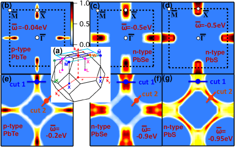
In order to elucidate ARPES data, we first consider the bulk Brillouin Zone (BZ) of PbQ, which has a face centered cubic (fcc) crystalline structure. This BZ is represented in Fig. 1a. Since PbQ is preferentially cleaved along (001) plane, one needs to pay attention to its square surface BZ projected onto the (001) plane for interpreting ARPES data. As shown in Fig. 1a, the and points project on the () and of the surface BZ. In Figs. 1b1g, we show constant-energy ARPES intensity maps , data as a function of in-plane momentum components and at a fixed , where is electronic energy with respect to . Figs. 1b and 1e correspond to -40 meV and = -200 meV respectively for a - type PbTe sample. As expected, -centered hole pockets derived from UVBs are clearly visible around at = -40 meV (Fig. 1b). When is changed to -200 meV, there is a remarkable change in topology of the intensity map via appearance of tube like regions connecting these isolated pockets (Fig. 1e). These tubular regions at higher have been predicted in several band structure calculations DJS ; SVANE ; FS_PBTE and have also been seen in recent ARPES measurements on Pb1-xSnxTe Hasan_PbTe and SnTe LITTLEWOOD . Qualitatively, similar evolution of intensity maps with are observed in Figs. 1c and 1f for PbSe, and in Figs. 1d and 1g for PbS.
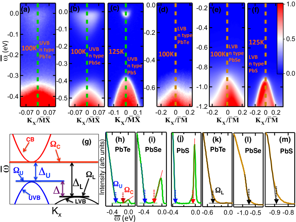
To further investigate the valence band structure of these materials, we concentrate on Fig. 2. Here electronic dispersions along two specific momentum space cuts, namely cut 1 and cut 2 defined in Fig. 1, are presented. Fig. 2a2c correspond to dispersion ( vs ) intensity maps along cut 1, while Figs. 2d2f to those along cut 2. One can recognize an electron band, the conduction band, separated in energy and momentum from a hole band, the UVB, in each intensity map along cut 1. On the contrary, a hole band alone is present along cut 2. By comparing data along cut 1 and cut 2, it can be immediately realized that the hole bands along cut 1, the UVBs, are distinct from those along cut 2, which we identify as the so-called LVBs. These clearly corroborate the two-band picture of PbQ.
Now, we will determine band gaps associated with LVBs and UVBs in various PbQ samples by examining Energy Distribution Curves (EDCs) HUFNER at momentum locations where these hole bands reach their individual maxima (Figs. 2h2m). In this context, an EDC is the distribution of electrons as a function of at a given . For the purpose of quantifying band gaps corresponding to a LVB or a UVB in a sample, we need to adopt some method of detecting not only the positions of their maxima, but also the position of the bottom of the conduction band (Fig. 2g). We illustrate this in Fig. 2h. It is easy to notice that the intensity of the EDC below a certain value of builds up abruptly on top of its background value and from then on it continues to grow almost linearly. We define this particular as and this marks the location of the top of the UVB. Similarly, one can also note a relatively sharp rise in intensity on top of the background above a certain value of . We refer this as and this corresponds to the bottom of the conduction band. Once we determine and , it is straightforward to evaluate the band gap of the UVB using =- (Fig. 2g). Following the same procedure we locate , the position for the top of a LVB, and calculate the relevant band gap using =- (Fig. 2g). Since each of these samples does not have the exact same carrier concentration, the useful quantity to be compared is =-, or in other words the energy separation between the maximum of a LVB and that of a UVB. Table I demonstrates that is largest for PbS ( meV) and smallest for PbTe ( meV), while in between ( meV) for PbSe at K.
| Materials | (meV) | (meV) | (meV) |
| PbTe | 190 | 320 | 130 |
| PbSe | 206 | 600 | 394 |
| PbS | 310 | 846 | 536 |
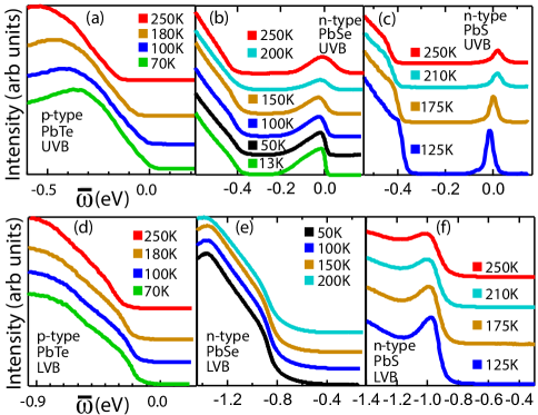
The objective of the remainder of the paper is to interrogate the impact of increasing on LVBs and UVBs. This is summarized in Figs. 3 and 4. In Figs. 3b and 3c we plot EDCs for - type PbSe and PbS samples respectively as a function of at the momentum locations of the top of their individual UVBs, while in Figs. 3e and 3f at those of their LVBs. We also display similar plots for the - type PbTe sample in Figs. 3a, 3d. Following the procedures described in Fig. 2, we obtain and as a function of for both PbSe and PbS and then plot them in Figs. 4a, 4b. Although does not change appreciably with , grows almost linearly with rising , which is consistent with positive temperature coefficients of band gap found by optical experiments in PbQ Miller1961 ; Tauber1966 ; Tsang1971 ; Snyder2013 . It is worth mentioning that such positive rate of change of band gap with in PbQ is contrary to what occurs in a majority of semiconductors. In fact, this “anomaly” helps PbQ to achieve high thermoelectric efficiency since it can mitigate the bipolar effects from intrinsic carrier activation. The later is responsible for the suppression of thermoelectric figure of merit at high in a material. We further point out that for the - type PbTe sample can’t be determined since its conduction band lies in the un-occupied side of the band structure. We can, however, obtain and from Fig. 3a and Fig. 3d respectively and thus, plot =- as a function of for PbTe along with PbSe and PbS in Fig. 4c.
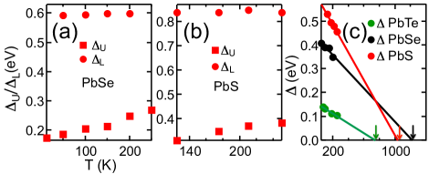
It is easy to infer that for each PbQ sample decreases monotonically with increasing (Fig. 4c). Data points within the measured values can be well represented by straight lines. If we assume that this linear change of with for each sample persists even above the highest measured temperature, we can extrapolate these straight lines and conclude that at certain characteristic temperature , will reduce to zero. This means that the band edge of the UVB will cross through that of the LVB at . An examination of Fig. 4c implies that K, K and K for PbTe, PbSe and PbS respectively. Although our estimation of involves an extrapolation over a large range, surprisingly the value for PbTe obtained from our ARPES experiments matches reasonably well with value from recent magnetic and optics measurements Heremans2013 ; Snyder2013 . Moreover, the value obtained for PbS also agrees well with that in Ref. 24, however, there is slight discrepency in case of PbSe. All these results suggest that PbTe, PbSe and PbS should become semiconductors with indirect band gap for , where the heavy hole LVB rises in energy above the light hole UVB. In this scenario, the charge transport in these materials should be dominated by the heavy holes created due to thermal excitations as the temperature approaches and consequently, the energy gap between LVB and UVB becomes comparable with k.
U.C. acknowledges support from the startup fund provided by the University of Virginia. Work at Argonne National Laboratory (C.D.M., D.Y.C., S.R., M.G.K.) was supported by the U.S. Department of Energy, Office of Basic Energy Sciences, Division of Materials Science and Engineering. U.C. thanks S.D. Mahanti for helpful discussions.
References
- (1) C. J. Vineis, A. Shakouri, A. Majumdar, and M. G. Kanatzidisl, Adv. Mater. 22, 3970 (2010).
- (2) Y. Pei, A. D. LaLonde, N. A. Heinz, and G. J. Snyder, Adv. Energy Mater. 2, 670 (2012).
- (3) M. S. Dresselhaus et al., Adv. Mater. 19 1043 (2007).
- (4) L. Zhao, V. P. Dravid, M. G. Kanatzidis, Energy Environ. Sci. 7, 2014 (2014).
- (5) M. G. Kanatzidis, Chem. Mater. 22, 648 (2010).
- (6) A. D. LaLonde, Y. Pei, and G. J. Snyderl, Energy Environ. Sci. 4, 2090 (2011).
- (7) S. Johnsen et al., J. Am. Chem. Soc. 133, 3460 (2011).
- (8) S. N. Girard et al., J. Am. Chem. Soc. 133, 16588 (2011).
- (9) Y. Pei et al., Nature 473, 66 (2011).
- (10) K. Biswas et al., Energy Environ. Sci. 4, 4675 (2011).
- (11) K. Biswas et al., Nat. Chem. 3, 160 (2011).
- (12) E. S. Bozin et al., Science 330 1660 (2010).
- (13) L. Fu, Phys. Rev. Lett. 106, 106802 (2011).
- (14) S. Y. Xu et al., Nat. Commun. 3, 1192 (2012).
- (15) Y. Tanaka et al., Nat. Phys. 8, 800 (2012).
- (16) P. Dziawa et al., Nat. Mater. 11, 1023 (2012).
- (17) Y. Okada et al., Science 341, 1496 (2013).
- (18) Y. Matsushita, H. Bluhm, T. H. Geballe, and I. R. Fisher, Phys. Rev. Lett. 94, 157002 (2005).
- (19) A. A. Andreev and V. N. Radionov, Sov. Phys. Semicond. 1, 145 (1967).
- (20) H. Sitter, K. Lischka, and H. Heinrich, Phys. Rev. B 16, 680 (1977).
- (21) Y. I. Ravich, B. A. Efimova, and V. I. Tamarchenko, Phys. Status Solidi B 48, 11 (1971).
- (22) Y. I. Ravich, B. A. Efimova, and V. I. Tamarchenko, Phys. Status Solidi B 48, 453 (1971).
- (23) C. M. Jaworski et al., Phys. Rev. B 87, 045203 (2013).
- (24) Z. M. Gibbs et al., Appl. Phys. Lett. 103, 262109 (2013).
- (25) Nv. Kolomoet, Mn. Vinograd, and L. M. Sysoeva, Sov. Phys. Semicond. 1, 1020 (1968).
- (26) R. S. Allgaier and B. B. Houston Jr, J. Appl. Phys. 37, 302 (1966).
- (27) C. E. Ekuma, D. J. Singh, J. Moreno, and M. Jarrell, Phys. Rev. B 85, 085205 (2012).
- (28) D. J. Singh, Phys. Rev. B 81,195217 (2010).
- (29) S. Hufner,Photoelectron Spectroscopy (Springer, New York, 1995).
- (30) V. Hinkel et al., Phys. Rev. B 40, 5549 (1989).
- (31) K. Nakayama, T. Sato, T. Takahashi, and H. Murakami, Phys. Rev. Lett. 100, 227004 (2008).
- (32) A. Svane et al., Phys. Rev. B 81, 245120 (2010).
- (33) B. Wiendlocha, Phys. Rev. B 88, 205205 (2013).
- (34) P. B. Littlewood et al., Phys. Rev. Lett. 105, 086404 (2010).
- (35) E. Miller, K. Komarek, and I. Cadoff, J. Appl. Phys. 32, 2457 (1961).
- (36) R. N. Tauber, A. A. Machonis, and I. B. Cadoff, J. Appl. Phys. 37, 4855 (1966).
- (37) Y. W. Tsang and M. L. Cohen, Phys. Rev. B 3, 1254 (1971).