Design and operation of a cryogenic charge-integrating preamplifier for the MuSun experiment
Abstract
The central detector in the MuSun experiment is a pad-plane time projection ionization chamber that operates without gas amplification in deuterium at 31 K; it is used to measure the rate of the muon capture process . A new charge-sensitive preamplifier, operated at 140 K, has been developed for this detector. It achieved a resolution of 4.5 keV(D2) or 120 RMS with zero detector capacitance at 1.1 µs integration time in laboratory tests. In the experimental environment, the electronic resolution is 10 keV(D2) or 250 RMS at a 0.5 µs integration time. The excellent energy resolution of this amplifier has enabled discrimination between signals from muon-catalyzed fusion and muon capture on chemical impurities, which will precisely determine systematic corrections due to these processes. It is also expected to improve the muon tracking and determination of the stopping location.
keywords:
Front-end electronics for detector readout; Analogue electronic circuits; Time projection chambers1 Introduction
The MuSun experiment [1] at the Paul Scherrer Institute (PSI) will provide a high-precision measurement of the nuclear capture rate of negative muons by deuterons (), a fundamental reaction that calibrates effective field theories of two-nucleon weak interactions [2]. Muons are stopped within a pad-plane time projection chamber (TPC) where deuterium gas is both the target material and the active medium of the detector. Each muon is tracked by the TPC to its stopping point, and only those muons that stop in the pure deuterium, away from the chamber walls, are accepted for later analysis. This technique is based in part on the experience derived from the TPC in the MuCap experiment [3], which was the predecessor of MuSun.
The TPC’s 48 pads, placed at a pitch of 16 mm 18 mm, are arranged in a 68 array, as shown in Figure 1. The TPC detects not only muon stops but also the products of muon-catalyzed fusion, as well as the recoil nuclei following muon capture on chemical impurities in the gas. Table 1 gives the scale of characteristic energy deposits from each of these processes.111Fusion occurs from molecular states and leads to monoenergetic recoils. Muon capture on impurities produces continuous recoil energy distributions which must be determined experimentally. The estimates for the characteristic energy scale of these processes are based on the simplest case that an excited daughter nucleus recoils against the neutrino. We are motivated to improve the energy resolution of the chamber to its physical limit in order to be able to separate capture on nitrogen and oxygen impurities from fusion to the 3He + final state. In this way, the TPC itself is used to monitor the purity of the deuterium. The improved resolution also provides a more precise determination of the muon stopping point, which is determined by comparing the energy deposited in the last and next-to-last pads in the track. It may even provide a method to identify the muon stopping point based on a definition that does not rely on the final pad at all, instead using an extrapolation of the much smaller energy deposits in upstream pads to project the location of the Bragg peak. This method would reduce the sensitivity of the measurement to the muon-catalyzed fusion pulses, which appear near the muon stopping point.
(a)

(b)
| Process | Energy scale (MeV) | Visible energy scale (MeV) |
|---|---|---|
| stop | 0.2 to 0.8 per pad | 0.2 to 0.8 per pad |
| + 3He + | 0.82 | 0.35 |
| He + | 0.80 | 0.53 |
| + + | 1.01 () + 3.02 () | 0.8 () + 3.0 () |
| N 14C* + | 0.30 | 0.14 |
| O 16N* + | 0.26 | 0.14 |
In order to minimize the number of these muon-catalyzed fusion pulses, the deuterium is cooled to 31 K. This temperature is just above the liquefaction point for its pressure of 5.1 bar, giving a density of 6.4% of liquid hydrogen. The purity of the deuterium must be maintained at the level of 1 part per billion (ppb), so the materials that contact the gas were selected for minimal outgassing, and the gas is continuously circulated through a cryogenic absorber [4]. Because the capture rate scales approximately as [5], contamination with nitrogen or oxygen increases the measured capture rate by about 2 s-1 per ppb. Consequently, even a very small impurity concentration will require a significant correction, in comparison to the experiment’s target precision of 6 s-1.
The drift field in the TPC is generated by a cathode plane, 72.4 mm above the pads, that is held at -80 kV; this gives a maximum drift time of 13.5 µs from the top of the chamber. A Frisch grid [6], at -3.5 kV, is 1.5 mm above the pads, which are at ground potential. There is no gas amplification in this arrangement; the Frisch grid improves the time resolution and eliminates the dependence of the pulse amplitude on the position of the ionization.
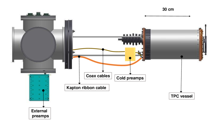
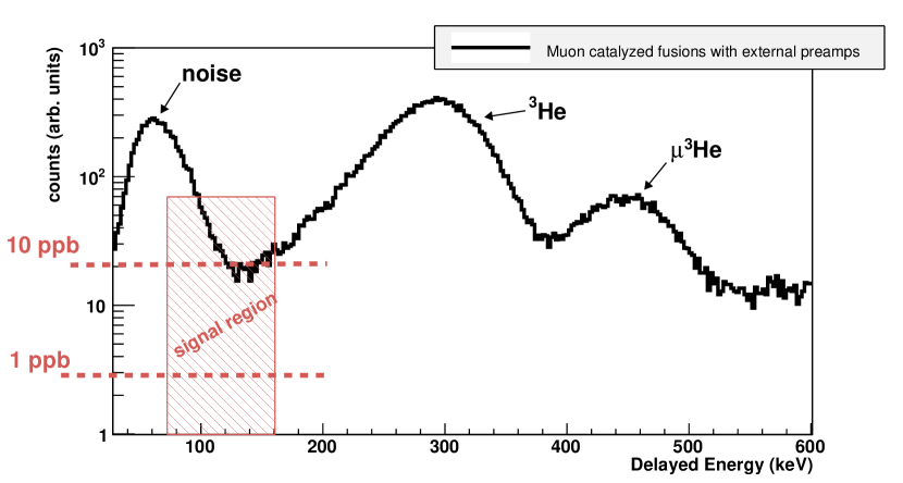
The cryogenic TPC is placed in an insulating vacuum. In initial runs of the experiment, external room-temperature preamplifiers were mounted outside the vacuum as shown in Figure 1. Each pad requires a separate amplifier, so there are 48 channels at each stage of the electronics chain. This arrangement required a 1 m in-vacuum cable to the nearest accessible flange. In order to limit its contribution to the detector capacitance, this long flexible Kapton ribbon cable was not shielded. Figure 2 shows that the sensitivity to impurities with this external preamplifier was limited to the 10 ppb level. In this paper, we describe our development of an in-vacuum cryogenic preamplifier system that allowed the long unshielded cable to be eliminated. The new preamplifier design improved the electronic part of the resolution of the detector by a factor of 3, and the use of shielded cables eliminated interference from microphonic pickup of the drift cathode high voltage on the long cable.
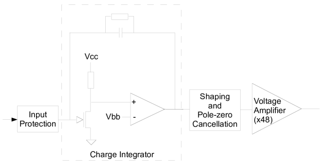
A block diagram of the new preamplifier is shown in Figure 3. A pair of diodes clamps the input signal voltage to protect the amplifier from currents induced by high voltage discharges inside the TPC. The first amplifying stage integrates the charge that reaches the gate of a junction field-effect transistor (JFET) that is inside a feedback loop regulated by an operational amplifier. A first level of pulse shaping is required for compatibility with the existing shaping amplifiers; it is applied before the the output is driven by a voltage gain stage.
2 Energy resolution
Ionization of deuterium requires eV per electron/ion pair [10, 11], an order of magnitude larger than in a semiconductor detector. A 1 MeV energy deposition in deuterium therefore corresponds to 27400 electrons. For such an event, the anticipated Fano factor of [12] would give as a physical limit an RMS resolution of = 90 electrons or 3.3 keV(D2). Recombination of electrons and ions due to space-charge density effects is minimal for muon tracks. Approximately half of the charge deposited by a nucleus such as 3He is lost to this recombination, because of the large . Recombination at that level would increase the optimal physical resolution to 110 electrons or 4.0 keV(D2) RMS for that peak. However, it is widened much further by a long non-Gaussian tail on the low-energy side, because the recombination fraction depends on the angle of the ionization track relative to the applied electric field [13]. It was therefore determined that a reasonable design goal would be a resolution at the level of 10 keV(D2) RMS, which would provide a substantial improvement relative to the 29 keV(D2) RMS of the existing room-temperature preamplifier.
Tests of the amplifier were performed by two groups at different institutions with somewhat different laboratory setups. The best purely electronic resolution that was observed for the new amplifier was 4.5 keV(D2), or 120 electrons, RMS. This result was obtained for a prototype where the protection diodes were omitted and no detector was connected. In this case, the preamplifier was cooled slowly by suspending it in the cold vapor just above the liquid level in a nitrogen dewar. An Ortec 485 amplifier with a shaping time of 1.1 µs (rather than the custom shaping amplifiers from the experiment) and a multichannel analyzer were used to collect the charge spectrum. A square-wave pulse was injected through the test input (a resistor divider and capacitive coupling to each channel), simulating approximately 1 MeV(D2) of energy deposition. The amplifier reached the optimal resolution at a temperature near 115 K. As shown in Figure 4, the resolution for the same amplifier at room temperature was 10 keV(D2) RMS. When a 47 pF ceramic capacitor was added, somewhat larger than the actual pad plane and cable capacitance of 10 pF, the optimal temperature increased slightly to 140 K. At this point, the resolution was 10 keV(D2) RMS; it was 16 keV(D2) RMS at room temperature. Comparable results were obtained by the other group.

The MuSun electronics must be optimized for a short shaping time, which is needed to resolve delayed fusion and impurity capture pulses from the initial muon stop pulse. These delayed pulses begin arriving immediately and decay with a fast component of 0.4 µs and a slow component of the 2.2 µs muon lifetime. The output of the preamplifier therefore drives a shaping amplifier that is a fifth-order Bessel filter with a 0.5 µs integration time; this device also includes a baseline restorer to remove low-frequency microphonic pickup.
In the experimental environment, the outputs of the shaping amplifier are connected to waveform digitizers that sample the signal at 50 MHz, and the pulse waveforms are fit to a template to extract the amplitude and integral. When the signal source is an electronic test pulser, the resulting spectrum is a Gaussian, illustrated in Figure 5. The result of fitting this distribution for each of the 48 pads is shown in Figure 6. The results reproduce those seen in the prototype laboratory tests: at room temperature, the typical resolution is 16 keV(D2) RMS, which improves to 10 keV(D2) RMS at the operating temperature of 140 K.

3 Amplifier design
The full schematic of the new amplifier is shown in Figure 7. A pair of BAV199 (NXP Semiconductors) diodes provides input protection. The first amplifying stage integrates the charge that reaches the gate of a BF862 (NXP Semiconductors) JFET, which is in a common-source configuration. It is inside a feedback loop regulated by one channel of an OPA2211 (Texas Instruments) operational amplifier, which maintains the quiescent bias of the JFET: , . The pulse is shaped by a first stage of filtering with pole-zero cancellation. Finally, the output is driven by a non-inverting voltage amplifier with a gain of 48.

3.1 Input protection
The input protection circuit has allowed the amplifiers to work reliably in an environment where discharges occur sporadically from the drift cathode to grounded components, inducing voltages on the pads. Initial prototypes used the BAV99 protection diode (a common part number; devices from Fairchild Semiconductor and NXP Semiconductor exhibited similar behavior), which increased the noise at room temperature. The BAV199 that was eventually employed is specified for three orders of magnitude lower leakage current and therefore makes a negligible contribution to the noise.
3.2 Field effect transistor
The most critical component that determines the noise performance is the field-effect transistor on the front end. Consequently, the design of the amplifier required testing and characterization of potential transistors. Other models that were considered included the BF998 dual-gate MOSFET and the BF861A and BF861B JFETs (NXP Semiconductor). Performance of the design with all of these devices was significantly worse than with the BF862 that was eventually chosen. As an example to show the scale of the effect, the resolution for the BF998 is shown in Figure 8. While this device seemed promising at room temperature with no input connected, the noise slope versus detector capacitance was not acceptable, and it did not improve with cooling.

3.3 Operational amplifier
The OPA2211 operational amplifier component was selected because we had successfully tested its single-channel counterpart, the OPA211, cooling it down to a temperature of 65 K where it turns off. Also, it is specified for a low voltage noise of 1.1 nV/ at room temperature. Excellent cryogenic performance was expected for it based on the BiCom3HV silicon-germanium (SiGe) heterojunction process [14] used in its fabrication. Individual SiGe transistors have been used in applications requiring temperatures as low as 4 K [15].
However, prototypes of two alternate designs of the amplifier were constructed and evaluated for comparison. One used the Amptek A250 low-noise amplifier block in place of the OPA2211 in the charge-integrating stage, and one replaced it with an amplifier with three discrete bipolar junction transistors. The A250 amplifier was tested at room temperature, and the transistor amplifier was tested both at room temperature and under cryogenic conditions. Both of these alternate designs provided energy resolutions that were essentially the same as the one that was eventually chosen. However, the OPA2211 is a much less expensive component than the A250, and the discrete transistor amplifier has a larger part count, which makes the circuit board layout less compact and may reduce its reliability.
3.4 Passive components
Care was used in the selection of resistors and capacitors. Thin-film and MELF resistors were used in preference to thick-film, which are known to exhibit excess noise above the Johnson-Nyquist limit. NP0/C0G dielectric, which has minimal temperature dependence, was preferred for all capacitors except some of the larger power filter bypass capacitors.
3.5 Shaping time constants
The dominant vibration frequency of the apparatus, which was driven by the cold-head compressor, is approximately 500 Hz; other modes with frequencies in the kHz have been seen. With the external preamplifiers, this frequency was picked up by the Kapton cable because it traveled parallel to the -80 kV drift cathode high voltage, creating a capacitor whose capacitance varied with vibration. However, similar pickup may originate inside the TPC between the Frisch grid and the pad plane. This acoustic frequency must be rejected at an early stage so that the preamplifier is not saturated by the oscillating baseline, which was previously seen at the level of several volts at the output.
The differentiation time constant between the two stages of the preamplifier is set to provide this filtering. It is determined by = 0.2 µs, so the -3 dB point of the highpass filter is at = 800 kHz. This provides substantial separation from the acoustic frequencies so that they are suppressed by many orders of magnitude.
A requirement of quick recovery to prepare for the next pulse, along with additional filtering of the acoustic frequencies, motivated the choice of the feedback resistor =20 M. While a larger feedback resistance would in principle introduce less noise, the discharge time constant of µs is matched to the requirement that the dynamic range of the charge-integrating stage should not be saturated when the next muon enters the TPC, typically 25 µs later. The pole-zero time constant =22 µs was tuned experimentally to optimize the cancellation of the long tail of the output pulse.
4 Noise spectrum and shaping time
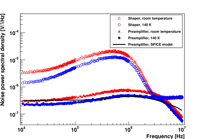
In order to interpret the noise of the preamplifier in terms of its frequency components, the noise power spectral density (PSD) was measured from Fourier transforms of the autocovariance of waveforms recorded with a digital oscilloscope. This noise spectrum, shown in Figure 9, agrees with a LTspice [16] circuit simulation model in the general shape, and it quantitatively agrees within a factor of 2. The model indicates that the largest contribution to the low-frequency voltage noise is from the parallel resistance , which discharges the charge-integrating stage. The largest contribution to the high-frequency side is the input voltage noise of the JFET.
We used the PSD to predict the dependence of the resolution on the external shaping time. For this purpose, the PSD was measured with bypassed to remove the early differentiation stage. The measured spectrum was folded with the transfer function of a shaping amplifier and integrated over frequency [7]
| (1) | |||||
| (2) |
to give a prediction of the total effective voltage noise as a function of the shaping time . In this calculation, was taken to be 3, which matched the observed output pulse shape from the shaping amplifier.
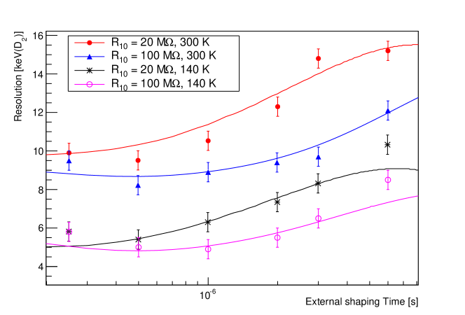
After normalization to units of energy, appears in Figure 10. This integration demonstrates that the noise spectrum corresponds to an optimal shaping time near the 0.5 µs that is required, which was confirmed by direct measurements of the resolution as a function of the shaping time set on an Ortec 673 amplifier. These measurements were performed with both 20 M and 100 M discharge resistor () values. They show that the impact on the resolution of the 20 M discharge resistor is minimal for short shaping times.
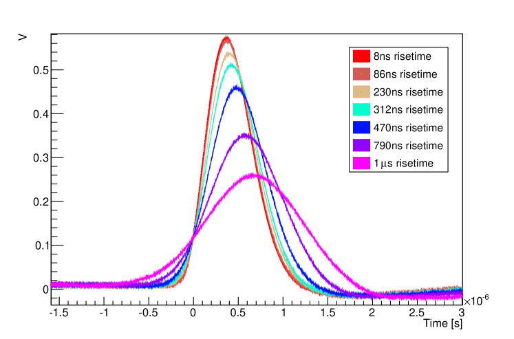
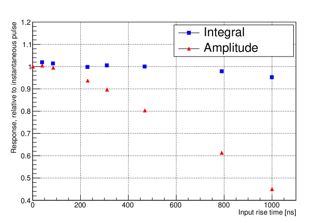
The short shaping time leads to a dependence of the width of the shaped pulse on the rise time over which the input charge is collected, as shown in Figure 11. This leads to a significant reduction in the amplitude: 55% over 1 µs. However, because the full waveform of the output of the shaping amplifier is recorded, it is possible in the analysis to integrate the pulse shape. The integral remains stable versus risetime for 0.5 µs and decreases by only 5% over 1 µs.
(a)
(b)
5 Installation and reliability
Four channels of a prototype version of the amplifier were deployed in an engineering run in 2012. These prototypes had only two channels per board, so the layout was not as compact as the final version, and some component values were different. The shaping time constant on the preamplifier was set to 100 µs rather than 0.2 µs, effectively bypassing the internal shaping stage, in order to be able to use off-the-shelf amplifiers where the shaping time could be varied. Consequently, the acoustic pickup was not fully suppressed. They were cooled to 260 K by contact with the long stainless steel support rods for the TPC, which is held at 31 K. Two channels were connected to the TPC by coaxial cables and two by unshielded wires. However, even the coaxial cable was not fully shielded, with 1 cm of bare conductor near the feedthrough to the TPC. Microphonic pickup was still evident; the signal amplitudes at the preamplifier output were 0.9 V on the coaxial channels and 1.8 V on unshielded channels.
All 48 pads were instrumented for the 2013 data collection run. The final version of the preamplifier card had to be quite compact to allow this number of channels to fit in the small space that was available. Each card holds eight channels, which are independent except for common power supply filtering and a test input. Each board is enclosed in a grounded aluminum box, mm3, as shown in Figure 12. The input and output signals pass through MMCX connectors on the board; RG178 coaxial cable is used to connect through the vacuum to DB-50 feedthrough connectors on the TPC and on the outside. The signal is fully enclosed by a ground shield all the way to the feedthrough into the TPC; this change, together with the change to the shaping time constant, suppressed the microphonic pickup to an undetectable level.
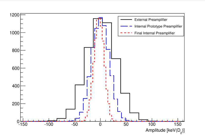
The preamplifier boxes are cooled by contact with a copper block, into which cold gas from liquid nitrogen boiloff is introduced. The flow of nitrogen is regulated by a needle valve to select the desired temperature, which is monitored by PT100 sensors attached to two of the boards. The power consumption of the entire set of 48 channels is 3.4 W at room temperature, decreasing by a factor of 2 at cryogenic temperatures, so the heat is easily removed in this way. Indeed, low power consumption was one of the initial design requirements because we had initially envisioned cooling them with our primary cryogenic system by thermal coupling to the 31 K deuterium, and only a few watts of spare capacity are available in that system. Figure 5 shows the improvement in energy resolution that was achieved with respect to the original external room-temperature amplifier system and to the partially-cooled prototype.
During the main production period of the 2013 run, the preamplifiers worked reliably; all 48 channels operated for a 48 day period. However, previous experience demonstrated two failure modes: discharges from the Frisch grid to the pad, and mechanical failure from overly rapid cooling. To avoid these problems in the future, the Frisch grid will be rebuilt with higher precision, and the protocol for cooling limits the rate to K per minute.
(a) 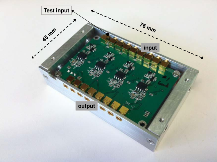
(b) 
6 Conclusion
The performance of the new MuSun preamplifier compares well to other preamplifiers used in state-of-the-art nuclear physics experiments. The resolution was measured to be 4.5 keV(D2) (120 electrons) RMS with no detector capacitance and a 1.1 µs shaping time, or 10 keV(D2) (250 electrons) RMS with a 0.5 µs shaping time in the experimental environment. As a point of comparison, the preamplifier designed for the GERDA neutrinoless double beta decay experiment reported 3 keV(Ge) FWHM resolution with a 33 pF detector capacitance at a 1 µs shaping time in liquid argon [17] at 87 K. This resolution corresponds to 430 electrons RMS or 16 keV(D2); it improves by a factor of 3 at the longer shaping times for which it is optimized. The commercial thermoelectrically cooled Amptek A250CF is advertised with a resolution of “76 electrons RMS,” or 2.8 keV(D2), but at a shaping time of 2 µs [18].
Reliable operation of the preamplifiers is essential, since they are time-consuming to access for repair. This reliability was achieved in the 2013 MuSun data collection period. The full set of 48 preamplifier channels operated reliably for a continuous period of 48 days of data collection and technical and systematic studies.
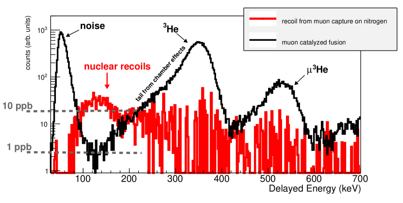
The primary motivation for the development project was to enable the MuSun TPC to be used as an in-situ impurity monitoring tool to measure chemical impurities in the deuterium at the part-per-billion scale. An energy spectrum of delayed pulses after the muon stop is shown in Figure 13. The deuterium gas was contaminated with 20 parts per billion of nitrogen at the time this spectrum was collected. The dramatically improved resolution in this spectrum may be seen by comparison with Figure 2; the gas density is also different, so the features are not at precisely the same energies, due to recombination effects. The RMS width of the 3He fusion peak is 17 keV(D2). Crucially, the signal from the nuclear recoils following muon capture is clearly visible at an energy of 125 keV, separated from the noise peak at lower energies and from the fusion products at higher energies. This measurement indicates that the new preamplifiers allow sensitivity to impurities at the 1 ppb level, providing an order-of-magnitude improvement over the room temperature preamplifiers.
Acknowledgments We gratefully acknowledge the work of all of our MuSun collaborators, and we thank them for permitting us to use the MuSun data in this publication. We thank PSI for beam time and important experimental resources. This work was supported in part by the National Science Foundation (grant number PHY-1206039) and the U.S. Department of Energy (grant number DE-FG02-97ER41020). We thank Uwe Greife of the Colorado School of Mines and Bernhard Lauss of PSI for support in testing early prototypes.
References
- [1] MuSun Collaboration, V. Andreev et al., Muon capture on the deuteron – the MuSun experiment, arXiv:1004.1754.
- [2] P. Kammel and K. Kubodera, Precision muon capture, Ann. Rev. Nucl. Part. Sci. 60 (2010) 327–353.
- [3] J. Egger et al., A high-pressure hydrogen time projection chamber for the MuCap experiment, arXiv:1405.2853.
- [4] V. A. Ganzha et al., A circulating hydrogen ultra-high purification system for the MuCap experiment, Nucl. Instrum. Meth. A578 (2007) 485–497, [arXiv:0705.1473].
- [5] D. F. Measday, The nuclear physics of muon capture, Phys. Rept. 354 (2001) 243–409.
- [6] O. Bunemann, T. E. Cranshaw, and J. A. Harvey, Design of grid ionization chambers, Can. J. Res. 27A 191–206.
- [7] H. Spieler, Semiconductor Detector Systems. Oxford University Press, 2005.
- [8] W. Blum, W. Riegler, and L. Rolandi, Particle Detection with Drift Chambers. Springer, 2008.
- [9] H. J. Hilke, Time projection chambers, Rep. Prog. Phys. 73 (2010) 116201.
- [10] International Commission on Radiation Units and Measurements, Average Energy Required to Produce an Ion Pair, ICRU report 31. 1979.
- [11] I. Smirnov, Modeling of ionization produced by fast charged particles in gases, Nucl. Instrum. Meth. A554 (2005) 474–493.
- [12] I. K. Bronic, On a relation between the W value and the Fano factor, J. Phys. B 25 (1992) L215.
- [13] R. Acciarri et al., A study of electron recombination using highly ionizing particles in the ArgoNeuT liquid argon TPC, J. Inst. 8 (Aug., 2013) 8005P, [arXiv:1306.1712].
- [14] W. Schwartz et al., BiCom3HV - a 36V complementary SiGe bipolar- and JFET-technology, in Bipolar/BiCMOS Circuits and Technology Meeting, pp. 42–45, 2007.
- [15] A. Joseph, J. Cressler, and D. Richey, Operation of SiGe heterojunction bipolar transistors in the liquid-helium temperature regime, Elec. Dev. Lett. 16 (1995) 268–270.
- [16] http://www.linear.com/designtools/software/#LTspice .
- [17] S. Riboldi et al., A low-noise charge sensitive preamplifier for Ge spectroscopy operating at cryogenic temperature in the GERDA experiment, in Nuclear Science Symposium Conference Record (NSS/MIC), pp. 1386–1388, Oct, 2010.
- [18] http://www.amptek.com/pdf/coolfet.pdf .