Wireless Josephson Amplifier
Abstract
Josephson junction parametric amplifiers are playing a crucial role in the readout chain in superconducting quantum information experiments. However, their integration with current 3D cavity implementations poses the problem of transitioning between waveguide, coax cables and planar circuits. Moreover, Josephson amplifiers require auxiliary microwave components, like directional couplers and/or hybrids, that are sources of spurious losses and impedance mismatches that limit measurement efficiency and amplifier tunability. We have developed a wireless architecture for these parametric amplifiers that eliminates superfluous microwave components and interconnects. This greatly simplifies their assembly and integration into experiments. We present an experimental realization of such a device operating in the GHz band with about MHz of amplitude gain-bandwidth product, on par with devices mounted in conventional sample holders. The simpler impedance environment presented to the amplifier also results in increased amplifier tunability.
pacs:
Parametric amplifiers (paramps) based on Josephson junctions Wahlsten, Rudner, and Claeson (1978); Mygind et al. (1979); Yurke et al. (1989), such as the Josephson Bifurcation Amplifier (JBA) and its degenerate amplifier relativesSiddiqi et al. (2004, 2005); Castellanos-Beltran and Lehnert (2007); Vijay (2008); Yamamoto et al. (2008); Castellanos-Beltran et al. (2008); Kamal, Marblestone, and Devoret (2009); Hatridge et al. (2011); Mutus et al. (2013); Zhong et al. (2013) and the Josephson Parametric Converter (JPC)Bergeal et al. (2010a, b); Abdo et al. (2011); Roch et al. (2012); Abdo, Kamal, and Devoret (2013); Schackert (2013), have become essential components in the quantum non-demolition (QND) readout chain of superconducting qubits. They have been instrumental in the experimental observation of quantum jumpsVijay, Slichter, and Siddiqi (2011), the detailed study of the quantum backaction of measurementHatridge et al. (2013); Murch et al. (2013), and feedbackVijay et al. (2012); de Lange et al. (2013), and will remain essential in future experiments aimed at quantum error correction and beyondSun et al. (2013); Devoret and Schoelkopf (2013). However, their integration into current state-of-the-art 3D circuit quantum electrodynamics (cQED) experimentsPaik et al. (2011); Rigetti et al. (2012) introduces the problem of interconnects that transition between waveguide, coaxial and planar microwave environments. Furthermore, these amplifiers require auxiliary microwave components such as directional couplers and/or hybrids to operate. These components introduce two problem: i) losses that reduce the system measurement efficiency and thus the fidelity of qubit readout; ii) a complicated frequency dependence of the impedance seen by the device which limits amplifier tunability and performance.
We radically simplify the design and implementation of an amplifier such as the JBA by coupling the lumped element Josephson circuit of the amplifier directly to the propagating mode of a rectangular waveguide using a dipole antenna. This design uses only low-loss, high quality materials commonly found in 3D superconducting qubits and eliminates printed circuit (PC) boards and wirebonds, as well as most of the auxiliary microwave components and interconnects. Their removal greatly simplifies the impedance seen by the device, making it flatter as a function of frequency, thus leading to improved amplifier tunability.
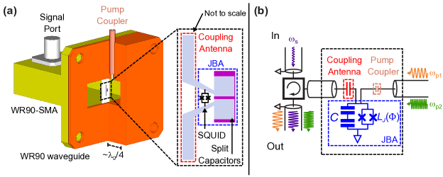
In this article, we describe the device, called the Wireless Josephson Amplifier (WJA). It is similar to the conventional JBA Hatridge et al. (2011); Vijay (2008) in that it consists of a lumped element resonator made of a superconducting quantum interference device (SQUID), acting as an external flux-tunable inductance cos, shunted by a split parallel-plate capacitor with capacitance (see Fig. 1). However, unlike the conventional implementation, a dipole antenna galvanically connected to the resonator couples it directly to the lowest-order propagating electromagnetic mode in a rectangular waveguide, which is chosen to be WR-90 (with inner dimensions of 0.90 inches by 0.40 inches) so that the WJA operates between and GHz. The chip is placed a quarter wavelength away from a wall - effectively a shorted termination - situating it at an electric field anti-node. Signals at frequency enter the device through a waveguide to coaxial cable (coax) adapter (used to make the device compatible with the existing experimental setup but will be eliminated in future experiments), traveling down the waveguide before exciting a differential signal across the resonator. This differential excitation makes the hybrids of the conventional implementation unnecessary. The pump tones at and required for stiff-pump amplificationKamal, Marblestone, and Devoret (2009) enter through a separate weakly coupled pump port, thereby eliminating the need for a directional coupler. Four-wave mixing in the non-linear resonator results in the signals at being amplified and re-radiated by the coupling antenna. The short ensures that all signals preferentially exit the device through the waveguide port.
Aside from the simplified design, the effective circuit representation of the WJA remains unchanged from the conventional implementationHatridge et al. (2011); Vijay (2008) except for one crucial aspect: the added dipole antenna to the WJA behaves like a coupling capacitor () between the resonator and the waveguide (see Fig. 1(b)). As a result, unlike the conventional JBA, the resonator bandwidth can be engineered independently of the resonator frequency because the coupling of the resonator is given by:
| (1) |
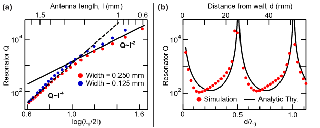
where is the impedance seen by the resonator which is a function of the chip distance from the wall, , is the characteristic impedance of the resonator, where is the stray inductance in the circuit. Thus, the resonator can be tuned controllably by changing , which in turn is proportional to the length of the dipole antenna, , in the limit of short lengths. To realize an amplifier designed for qubit readout, the circuit parameters were chosen to be A and pF for a maximum linear resonance frequency around GHz; in addition, to make the amplifier bandwidth larger than the typical qubit cavity bandwidth, we chose which required two antenna pads that were each mm long and mm wide separated by m gaps, sizes that can be readily fabricated using either optical or electron-beam lithography.
Although was chosen for this particular device, as shown in Fig. 2(a), the can be tuned by over three orders of magnitude by choosing between mm and mm. While the dependence can be calculated analytically, a finite element electromagnetic solver, such as HFSS111ANSYS HFSS version 15.1, was used for a more detailed analysis. These simulations confirmed that the behavior predicted by Eqn. 1 for short antenna lengths breaks down for longer antenna lengths when the size of the dipole antenna becomes comparable to the size of the waveguide. The behavior of the coupling as a function of the chip distance from the wall, , was also simulated; the coupling should be maximum when the chip is at an antinode of the electric field in the waveguide and minimum when it is at a node. As shown in Fig. 2(b), the simulations confirm the expected divergence in the when where is an integer and is the guide wavelengthPozar (2012); the diverges at these points because . Moreover, because the coupling is a flat function of (to first order) around , the design is robust against errors in fabrication or machining that affect the resonator frequency or its position from the wall.
Fabricating the lumped-element circuit for the WJA required making both parallel-plate capacitors and a Josephson junction on chip. The same three-layer fabrication process developed for conventional JBAsFrunzio (2006); Vijay (2008); Hatridge et al. (2011) was used to avoid the complication of making vias. First, a nm niobium layer was deposited on the wafer and patterned using optical lithography and reactive-ion etching to define the shared ground plane of the split parallel-plate capacitors. Next, nm silicon nitride was deposited conformally over the entire wafer using plasma-enhanced chemical vapor deposition to form the dielectric layer of the capacitors; the thickness and dielectric constant () of this layer are used to calculate the size of the capacitors needed for a pF capacitance. Finally, a bi-layer of electron-beam resist was spun on the wafer and patterned using electron-beam lithography. Double angle evaporation of aluminum was used to define the Josephson junctions in the m m SQUID loop as well as the top plates of the capacitors and the coupling antenna.
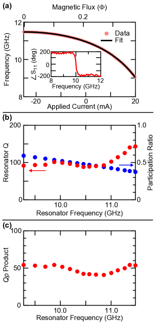
The WJAs were cooled down in a cryogen-free dilution refrigerator to about mK. First, the amplifier’s linear resonance frequency and bandwidth were measured by looking at the reflected phase using a vector network analyzer (VNA). The reflected phase (Fig. 3(a) inset) showed a phase roll characteristic of an overcoupled resonator. From this, the coupling was found to be as desired and agreeing with simulation results. Next, by applying current to an external superconducting coil magnet, the linear frequency of the WJA was tuned with flux. As shown in Fig. 3(a), the linear resonance frequency tuned from its maximum value of GHz down to GHz. By fitting the resonance frequency as a function of flux to the equation:
| (2) |
the circuit parameters were found to be pF, pH and A with error bars of about . The discrepancy in the measured capacitance from the desired value is a result of operating the circuit near the self-resonance frequency of the capacitor; in future iterations of the WJA, it would be advantageous to use thinner dielectric layers and/or larger dielectric constants to avoid this problem. Nevertheless, the device still operated in the desired frequency range. More importantly, as shown in Fig. 3(b), the varied by only between GHz and GHz. Above GHz, the changed rapidly because at these higher frequencies, the chip distance from the wall is significantly different from . The almost constant as a function of frequency not only agrees well with simulation results but also suggests that the environment’s impedance is well matched over the whole frequency range. Because the of the WJA can be varied by changing the antenna length independent of the device frequency, this architecture offers a valuable control knob over the amplifier bandwidth that is unavailable in conventional JBAs.
Another important figure of merit for single effective-junction parametric amplifiers is the inductance participation ratio, . Using the the extracted values of and , the was found to vary between about and over the entire frequency range (see blue trace in Fig. 3(b)). Together the and are important because their product determines both whether the resonator will amplify and the maximum signal power that can be amplified without saturationSchackert (2013). To realize an amplifier with sufficient gain for qubit readout, it is necessary that ; however, to maximize the amplifier saturation power, the -product needs to be as low as possible with to being optimalSchackert (2013). In particular, for the present device, the product was around by design. Since varies by only about over the whole frequency range (see Fig. 3(c)), this device is expected to show tunability and constant amplifier performance over the operation band. Combined with the increased control over the and in this architecture, this will allow for fuller optimization of the amplifier’s properties in future iterations.
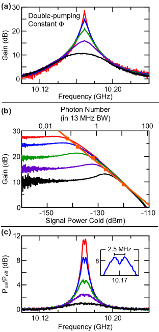
The WJA was characterized as a phase-sensitive amplifier by applying two pump tones, and , symmetrically detuned by MHz from the signal tone at through the weakly coupled pump port. Different gains at the same frequency were achieved by keeping the flux through the SQUID constant while changing the two pump powers. As shown in Fig. 4(a), the amplifier achieved gains between unity and over dB. In particular at dB of gain, the instantaneous amplifier bandwidth is MHz (much larger than typical cavity bandwidths used in qubit experiments).
The amplifier’s dynamic range was characterized by measuring its maximum gain as a function of input signal power from the VNA and finding the power at which the gain fell by dB (the power); at dB of gain, we found that the saturation power was dBm which corresponded to approximately photons in the MHz amplifier bandwidth (see Fig. 4(b)). Additionally, the slope of power versus gain (orange line in Fig. 4(b)) was dB/dB, close to the ideal slope of dB/dB expected for an ideal linear parametric amplifierAbdo et al. (2011). The dynamic range of this device, while comparable to conventional JBAs, could be further increased by reducing the -product by a factor of ten to ; while this could be done either by reducing the or the , the current is optimal for qubit readout and so reducing the participation ratio is desirable. This can be achieved, for example, by using multiple SQUIDs with larger and hence a smaller .
A final figure of merit, especially for parametric amplifiers, is the amplifier’s noise temperature, . According to CavesCaves (1982), when the WJA is operated as a phase-sensitive parametric amplifier, the added noise is zero for the amplified quadrature () while for the de-amplified quadrature. The noise temperature for this amplifier was estimated from the increase in the noise measured by a room temperature spectrum analyzer when the WJA was turned on. When the WJA was off, i.e , the noise measured at room temperature is entirely dominated by noise added by the high electron mobility transistor (HEMT) amplifier. On the other hand, when the WJA is turned on, the measured noise increases because the spectrum analyzer now also receives amplified quantum noise from the parametric amplifier. We call the noise visibility ratio the amount by which the combined noise of the WJA and the HEMT is greater than the HEMT noise alone.
As shown in Fig. 4(c), the noise visibility increased with WJA gain; when dB (blue trace), the ratio was about dB indicating that less than of the power at room temperature was added HEMT noise. The dips in the traces at the center frequency are a consequence of the WJA behaving as a phase-sensitive amplifier at . Since only one of the two quadratures is amplified, the measured noise should be dB lower. However, the finite resolution bandwidth of the spectrum analyzer smears out the dip and consequently, the measured dips were smaller than the expected dB (see inset of Fig. 4(c)) and have a width of MHz equal to the spectrum analyzer’s resolution bandwidth. At dB, the difference in noise power of dB was comparable to other parametric amplifiers, JBAs or JPCs, measured in this experimental setup indicating that the noise performance of the WJA is comparable to standard paramps. For this measurement setup, the system noise temperature, , which is the effective noise temperature of the HEMT and the losses between the plane of the WJA and the HEMT, is assumed to be K. From the measured increase of dB at dB, we estimate an upper bound on the noise added by the WJA of , where .
In conclusion, we have designed and operated a wireless implementation of a Josephson parametric amplifier for readout of a superconducting qubit in a 3D cavity. Our design replaces the usual connections between the chip of the amplifier and the qubit port by a simple on-chip antenna placed in the center of a waveguide. This leads to a much simplified assembly of critical components. The WJA exhibits the same gain, bandwidth, dynamic range and noise properties as a conventional JBA while also offering improved tunability and increased control over both the quality factor and participation ratio . With this better control, it is possible to increase the amplifier dynamic range with a WJA consisting of multiple SQUIDs in series with correspondingly large critical current junctions. The simplification of the microwave environment seen by the Josephson element should also eliminate sources of loss that currently limit the measurement efficiency of circuit QED experiments. The incorporation of a WJA in a qubit readout chain is currently under way. Finally, this architecture could be easily extended to realize a wireless JPC by adding dipole antenna to a lumped JPC circuit and placing it at the intersection of two waveguides with perpendicular polarizations.
Acknowledgements.
Fabrication assistance from M. Rooks, as well as the Yale Institute for Nanoscience and Quantum Engineering facilities are gratefully acknowledged. This research was supported by the National Science Foundation under Grants No. DMR-1006060 and No. DMR- 0653377, the US Army Research Office Grants No. W911NF-09-1-0514 and No. W911NF-14-1-0011.References
- Wahlsten, Rudner, and Claeson (1978) S. Wahlsten, S. Rudner, and T. Claeson, Journal of Applied Physics 49, 4248 (1978).
- Mygind et al. (1979) J. Mygind, N. F. Pedersen, O. H. Soerensen, B. Dueholm, and M. T. Levinsen, Applied Physics Letters 35, 91 (1979).
- Yurke et al. (1989) B. Yurke, L. R. Corruccini, P. G. Kaminsky, L. W. Rupp, A. D. Smith, A. H. Silver, R. W. Simon, and E. A. Whittaker, Phys. Rev. A 39, 2519 (1989).
- Siddiqi et al. (2004) I. Siddiqi, R. Vijay, F. Pierre, C. M. Wilson, M. Metcalfe, C. Rigetti, L. Frunzio, and M. H. Devoret, Phys. Rev. Lett. 93, 207002 (2004).
- Siddiqi et al. (2005) I. Siddiqi, R. Vijay, F. Pierre, C. M. Wilson, L. Frunzio, M. Metcalfe, C. Rigetti, R. J. Schoelkopf, M. H. Devoret, D. Vion, and D. Esteve, Phys. Rev. Lett. 94, 027005 (2005).
- Castellanos-Beltran and Lehnert (2007) M. A. Castellanos-Beltran and K. W. Lehnert, Applied Physics Letters 91, 083509 (2007).
- Vijay (2008) R. Vijay, Josephson Bifurcation Amplifier, Ph.D. thesis, Yale University (2008).
- Yamamoto et al. (2008) T. Yamamoto, K. Inomata, M. Watanabe, K. Matsuba, T. Miyazaki, W. D. Oliver, Y. Nakamura, and J. S. Tsai, Applied Physics Letters 93, 042510 (2008).
- Castellanos-Beltran et al. (2008) M. A. Castellanos-Beltran, K. D. Irwin, G. C. Hilton, L. R. Vale, and K. W. Lehnert, Nat. Phys. 4, 929 (2008).
- Kamal, Marblestone, and Devoret (2009) A. Kamal, A. Marblestone, and M. Devoret, Phys. Rev. B 79, 184301 (2009).
- Hatridge et al. (2011) M. Hatridge, R. Vijay, D. H. Slichter, J. Clarke, and I. Siddiqi, Phys. Rev. B 83, 134501 (2011).
- Mutus et al. (2013) J. Y. Mutus, T. C. White, E. Jeffrey, D. Sank, R. Barends, J. Bochmann, Y. Chen, Z. Chen, B. Chiaro, A. Dunsworth, J. Kelly, A. Megrant, C. Neill, P. J. J. O'Malley, P. Roushan, A. Vainsencher, J. Wenner, I. Siddiqi, R. Vijay, A. N. Cleland, and J. M. Martinis, Applied Physics Letters 103, 122602 (2013).
- Zhong et al. (2013) L. Zhong, E. Menzel, R. Di Candia, P. Eder, M. Ihmig, A. Baust, M. Haeberlein, E. Hoffmann, K. Inomata, T. Yamamoto, Y. Nakamura, E. Solano, F. Deppe, A. Marx, and R. Gross, New Journal of Physics 15, 125013 (2013).
- Bergeal et al. (2010a) N. Bergeal, R. Vijay, V. E. Manucharyan, I. Siddiqi, R. J. Schoelkopf, S. M. Girvin, and M. H. Devoret, Nat. Phys. 6, 296 (2010a).
- Bergeal et al. (2010b) N. Bergeal, F. Schackert, M. Metcalfe, R. Vijay, V. E. Manucharyan, L. Frunzio, D. E. Prober, R. J. Schoelkopf, S. M. Girvin, and M. H. Devoret, Nature 465, 64 (2010b).
- Abdo et al. (2011) B. Abdo, F. Schackert, M. Hatridge, C. Rigetti, and M. Devoret, Appl. Phys. Lett. 99, 162506 (2011).
- Roch et al. (2012) N. Roch, E. Flurin, F. Nguyen, P. Morfin, P. Campagne-Ibarcq, M. H. Devoret, and B. Huard, Phys. Rev. Lett. 108, 147701 (2012).
- Abdo, Kamal, and Devoret (2013) B. Abdo, A. Kamal, and M. H. Devoret, Phys. Rev. B 87, 014508 (2013).
- Schackert (2013) F. Schackert, A Practical Quantum-Limited Parametric Amplifier Based on the Josephson Ring Modulator, Ph.D. thesis, Yale University (2013).
- Vijay, Slichter, and Siddiqi (2011) R. Vijay, D. H. Slichter, and I. Siddiqi, Phys. Rev. Lett. 106, 110502 (2011).
- Hatridge et al. (2013) M. Hatridge, S. Shankar, M. Mirrahimi, F. Schackert, K. Geerlings, T. Brecht, K. M. Sliwa, B. Abdo, L. Frunzio, S. M. Girvin, R. J. Schoelkopf, and M. H. Devoret, Science 339, 178 (2013).
- Murch et al. (2013) K. W. Murch, S. J. Weber, C. Macklin, and I. Siddiqi, Nature 502, 211 (2013).
- Vijay et al. (2012) R. Vijay, C. Macklin, D. H. Slichter, S. J. Weber, K. W. Murch, R. Naik, A. N. Korotkov, and I. Siddiqi, Nature 490, 77 (2012).
- de Lange et al. (2013) G. de Lange, D. Ristè, M. J. Tiggelman, C. Eichler, L. Tornberg, G. Johansson, A. Wallraff, R. N. Schouten, and L. DiCarlo, arXiv:1311.5472 (2013).
- Sun et al. (2013) L. Sun, A. Petrenko, Z. Leghtas, B. Vlastakis, G. Kirchmair, K. M. Sliwa, A. Narla, M. Hatridge, S. Shankar, J. Blumoff, L. Frunzio, M. Mirrahimi, M. H. Devoret, and R. J. Schoelkopf, arXiv:1311.2534 (2013).
- Devoret and Schoelkopf (2013) M. H. Devoret and R. J. Schoelkopf, Science 339, 1169 (2013).
- Paik et al. (2011) H. Paik, D. I. Schuster, L. S. Bishop, G. Kirchmair, G. Catelani, A. P. Sears, B. R. Johnson, M. J. Reagor, L. Frunzio, L. I. Glazman, S. M. Girvin, M. H. Devoret, and R. J. Schoelkopf, Phys. Rev. Lett. 107, 240501 (2011).
- Rigetti et al. (2012) C. Rigetti, J. M. Gambetta, S. Poletto, B. L. T. Plourde, J. M. Chow, A. D. Córcoles, J. A. Smolin, S. T. Merkel, J. R. Rozen, G. A. Keefe, M. B. Rothwell, M. B. Ketchen, and M. Steffen, Phys. Rev. B 86, 100506 (2012).
- Note (1) ANSYS HFSS version 15.1.
- Pozar (2012) D. M. Pozar, Microwave Engineering (John Wiley & Sons Inc., 2012).
- Frunzio (2006) L. Frunzio, Design and fabrication of superconducting circuit for amplification and processing of quantum signals, Ph.D. thesis, l’Universite Paris-sud (2006).
- Caves (1982) C. M. Caves, Phys. Rev. D 26, 1817 (1982).