Epitaxial hexagonal boron nitride on Ir(111): A work function template
Abstract
Hexagonal boron nitride (h-BN) is a prominent member in the growing family of two-dimensional materials with potential applications ranging from being an atomically smooth support for other 2D materials to templating growth of molecular layers. We have studied the structure of monolayer h-BN grown by chemical vapour deposition on Ir(111) by low-temperature scanning tunneling microscopy (STM) and spectroscopy (STS) experiments and state-of-the-art density functional theory (DFT) calculations. The lattice-mismatch between the h-BN and Ir(111) surface results in the formation of a moiré superstructure with a periodicity of 29 Å and a corrugation of 0.4 Å. By measuring the field emission resonances above the h-BN layer, we find a modulation of the work function within the moiré unit cell of 0.5 eV. DFT simulations for a 13-on-12 h-BN/Ir(111) unit cell confirm our experimental findings and allow us to relate the change in the work function to the subtle changes in the interaction between boron and nitrogen atoms and the underlying substrate atoms within the moiré unit cell. Hexagonal boron nitride on Ir(111) combines weak topographic corrugation with a strong work function modulation over the moiré unit cell. This makes h-BN/Ir(111) a potential substrate for electronically modulated thin film and hetero-sandwich structures.
pacs:
68.37.Ef 68.90.+g 73.20.-r 73.22.-f 81.15.GhI Introduction
Hexagonal boron nitride (h-BN) is a prominent member in the growing family of two-dimensional materials. Isostructural to graphene while being a wide bandgap insulator, h-BN has found a host of current and potential applications. These range from serving as an atomically smooth support for other 2D materials to band structure engineering in graphene/h-BN heterostructures to epitaxial growth in two-dimensional space.Dean2010 ; Hunt2013 ; Liu2014 Another area of interest in h-BN are the so-called boron nitride nanomeshes - epitaxial monolayers of h-BN grown on transition metal surfaces.Corso2004 ; Laskowski2007 Various studies have been motivated by their ability to act as a template for bottom-up fabrication techniques while simultaneously providing electronic decoupling from the metallic substrate.Corso2004 ; Corso2005 ; Goriachko2007 ; Berner2007 ; Dil2008 ; Kahle2012 ; Joshi2012 ; Schulz2013 ; Joshi2013 The term “nanomesh” highlights the peculiar structure of the h-BN monolayers: Due to the lattice-mismatch with the underlying substrate, the atomic registry between the boron and nitrogen atoms and the metallic surface is periodically modulated, resulting in a moiré pattern formed by regions of stronger h-BN/metal and weaker h-BN/metal interaction.
Topography, work function and chemical reactivity are periodically modulated over the moiré pattern, which is the origin of the templating effect of the h-BN nanomesh. Recent work on extended, self-assembled molecular layers on h-BN/Ir(111) Schulz2013 and h-BN/Cu(111) Joshi2013 has demonstrated that these templating capabilities are not only limited to structural properties but can be extended to the electronic properties of the overlayer: The work function modulation along the h-BN moiré unit cell causes an energy shift of the molecular resonances,Joshi2013 potentially resulting in the local charging of the molecular layer.Schulz2013 Thus, monolayers of h-BN offer a route to grow novel organic thin films or layered heterostructures, with periodically modulated electronic properties. Three criteria control the properties of the resulting films: (i) structural corrugation of the h-BN layer, (ii) work function modulation along the moiré unit cell and (iii) coherence length of the moiré pattern. A small structural corrugation facilitates the growth of defect-free overlayers and sandwich structures, while a large work function modulation allows the patterning of electronic properties. Finally, growing high-quality, large-scale layers requires the h-BN to maintain a uniform moiré periodicity and orientation over the entire sample size with a low density of domain boundaries.
A low structural corrugation is generally found in weakly interacting h-BN/metal systems such as h-BN/Cu(111)Preo2005 ; Joshi2012 ; Roth2013 or h-BN/Pt(111) Preo2007 . However, the weak interaction often leads to the formation of several rotational domains,Mueller2005 ; Morscher2006 ; Mueller2010 ; Joshi2012 as there is no preferred growth direction. For example on copper, this leads to a variation of the moiré periodicity from ca. 5 nm up to 14 nm Joshi2012 , depending on the rotational alignment. This problem can be by-passed by growing h-BN on strongly interacting transition metals, which typically result in single-domain growth, as well as a larger work function modulation. The prototypical, strongly interacting nanomesh systems h-BN/Rh(111) Corso2004 ; Berner2007 ; Diaz2013 and h-BN/Ru(0001) Goriachko2007 ; Diaz2013 offer a work function modulation of up to 0.5 eV along the moiré, however, accompanied by a large structural corrugation of around 1 to 1.5 Å. A h-BN/metal system combining the advantages of strongly and weakly interacting systems would be of great value for further exploration of electronically modulated thin films.
Recent low-energy electron diffraction experiments Orlando2012 indicate the existence of a preferred orientation of h-BN on Ir(111), while previous density functional theory (DFT) calculations Laskowski2008 as well as X-ray adsorption and photoelectron spectroscopy experiments Preo2007 suggest a weaker interaction of h-BN with Ir(111) than with Rh(111) or Ru(0001). Thus, h-BN/Ir(111) constitutes a promising candidate to combine the desired properties of preferred orientation of the moiré superstructure, strong work function modulation and small structural corrugation. Here, we show that h-BN grown on Ir(111) indeed fulfills these criteria. Low-temperature scanning tunneling microscopy (STM) experiments demonstrate that h-BN/Ir(111) can be grown to form large domains extending across step edges, and with a preferred orientation of the h-BN layer with respect to the substrate lattice, resulting in a low spread of the moiré periodicity. Scanning tunneling spectroscopy (STS) indicates a modulation of the work function along the moiré unit cell of 0.5 eV. Our experimental findings are complemented by extensive, state-of-the-art DFT calculations. The computational results confirm the work function modulation and indicate a weak structural corrugation of the h-BN layer of 35 pm. Combining the experimental results with the simulation of the moiré unit cell, we can explain the work function modulation as a result of subtle changes in the registry and interaction between the h-BN and substrate atoms.
II Methods
Sample preparation. All the experiments were carried out in an ultra-high vacuum system with a base pressure of mbar. The (111)-terminated iridium single crystal was cleaned by repeated cycles of sputtering with 1.5 kV neon ions, annealing to 900 ∘C in mbar oxygen and subsequent flashing to 1400 ∘C. Full monolayers of h-BN were grown by thermal cracking of borazine (B3N3H6, Chemos GmbH) at the Ir(111) Orlando2012 substrate held at a temperature of 1080 ∘C and with a borazine pressure of mbar. With these parameters, the h-BN layer grows with a low nucleation density and forms large domains with sizes larger than the terrace width of the Ir(111) substrate.Lu2013 The resulting h-BN domains are aligned with the substrate lattice, resulting in a very uniform moiré periodicity of Å. When growing the h-BN at higher substrate temperatures between 1100 and 1200 ∘C, we also find misaligned domains, yielding moire periodicities down to 22 Å. Temperature programmed growth of the h-BN layer by preadsorption of borazine on the sample held at room temperatures and subsequent annealing results in a mosaic-growth Lu2013 of the h-BN, yielding a large spread of rotational domains, as well as defects and grain boundaries. Using sample temperatures significantly above 1200 ∘C suppresses the h-BN growth, potentially due to an increase in desorption of nitrogen from the Ir surface and solubility of boron into the Ir bulk.
STM measurements. After the preparation, the sample was inserted into the low-temperature STM (Createc LT-STM) and all subsequent measurements were performed at 5 K. Differential conductance (d/d) spectra are recorded by standard lock-in detection on the tunneling current while sweeping the applied sample bias with a peak-to-peak modulation of 20 mV at a frequency of 517 Hz, with the current feedback loop opened at 1 V and 0.25 nA. spectra were taken at a bias of 50 mV. Field emission resonances (FERs) were measured with closed feedback loop at a current setpoint of 0.5 nA. STM images and d/d line spectra were processed using the WSxM Horcas2007 and SpectraFox SpectraFox softwares, respectively.
DFT calculations. The DFT calculations were performed using the QuickStep module VandeVondele2005 of the CP2K package (http://www.CP2K.org/), where the Kohn-Sham orbitals are expanded in the basis of Gaussian functions (here, DZVP-MOLOPT-SR-GTH for B and N and DZVP-MOLOPT-SR-GTH-q17 for IrVandeVondele2007 ), and plane waves up to a cut-off energy of 700 Ry, REL_CUTOFF of 70 Ry, for the density. Generalised Gradient Approximation (GGA) revPBE Zhang1998 was employed as the exchange-correlation functional, and the missing London dispersion incorporated using the semi-empirical DFT-D3 formalism.Grimme2010 The surface was modelled using the slab approach with four layers of the substrate of which the two at the bottom were held fixed during the geometry relaxation, and the h-BN layer adsorbed only on one side of the slab. The length of the cell was 40 Å in order to decouple the two sides of the slab from each other. Only the point was used in the evaluation of the integrals over the first Brillouin zone, and the bulk lattice constant of 3.801 Å obtained with revPBE-D3 was used. The occupation numbers are broadened using the Fermi-Dirac distribution at 300 K around the Fermi energy. The STM images were simulated using the Tersoff-Hamann model Tersoff1985 with an s wave tip. Further details on the method can be found in Ref. Diaz2013,
III Results and Discussion
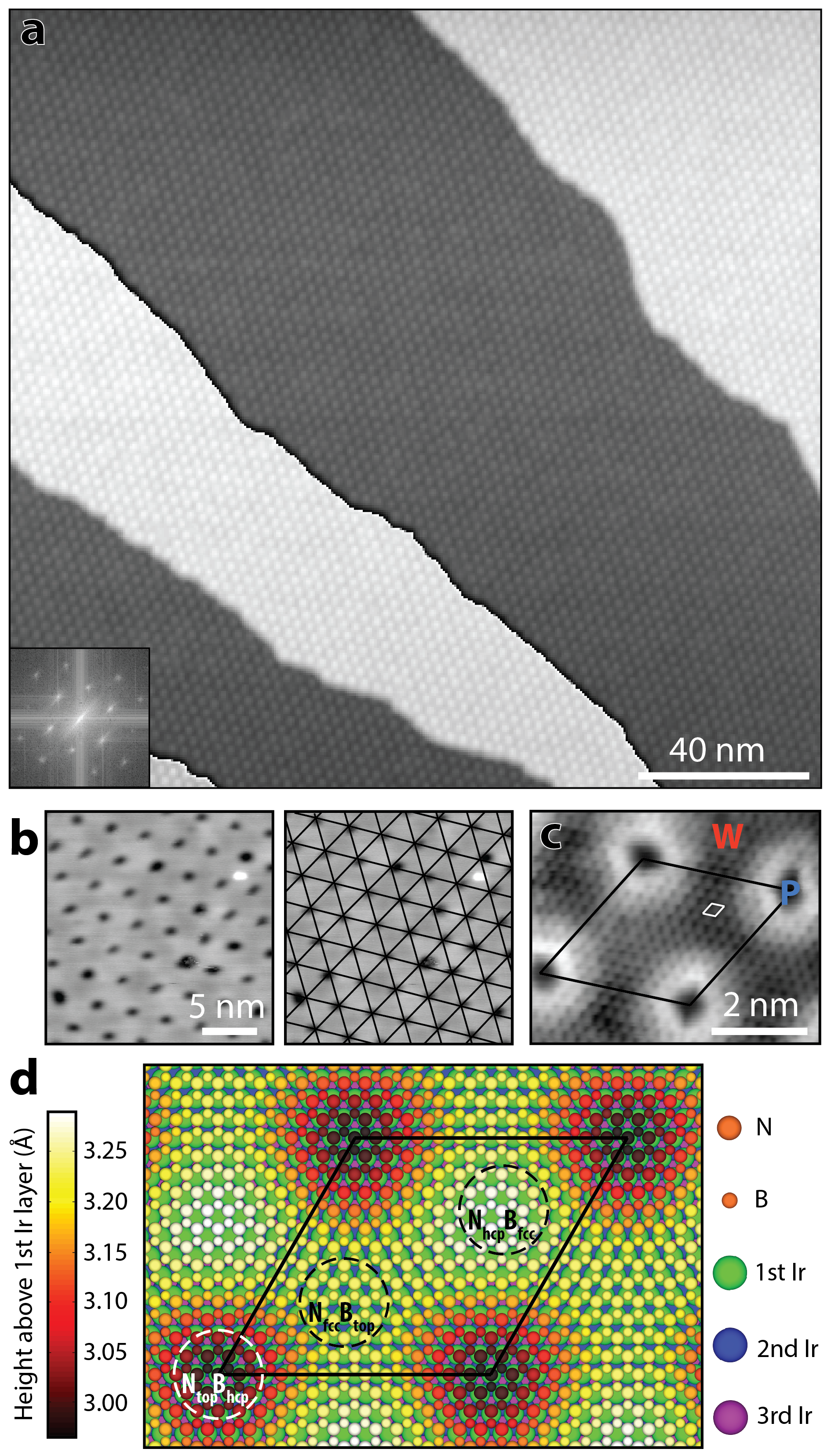
Figure 1a shows a large-scale STM image of monolayer h-BN grown on the Ir(111) surface by chemical vapor deposition (CVD) using borazine as the precursor (see Methods for details). A single domain extends over several monatomic steps, indicating the high quality of the h-BN layer as it extends over step edges in a carpet-like fashion.Coraux2008 ; Sutter2008 ; Lu2013 The moiré superstructure due to the lattice-mismatch (Ir(111): = 2.714 Å Singh1968 and h-BN: = 2.505 Å Pease1952 ) is highlighted in Figure 1b; it is formed by depressions arranged in a hexagonal lattice. The periodicity of the superstructure is indicated in the right panel of Figure 1b by a hexagonal grid overlayed onto the STM image. Throughout this article, we will use the common terminology and refer to the depressions of the moiré as pores and to the surrounding regions as wires. However, it is important to note that the h-BN forms a continuous, closed monolayer without any voids. The moiré unit cell as well as the atomic unit cell of the h-BN are depicted in the high resolution STM topograph in Figure 1c. As can be seen, the two unit cells are aligned, without any appreciable rotation with respect to each other. Since the angle between the moiré and h-BN lattice vectors represents a roughly ten-fold magnification of the rotation between the lattice of h-BN and Ir(111),NDiaye2008 we conclude that the misalignment between the two atomic lattices is less than 0.5 ∘. When growing the h-BN layer at a substrate temperature of 1080 ∘C, we only find aligned h-BN with a moiré periodicity of Å. The small deviation from the theoretical moiré periodicity of 32.5 Å suggests that the h-BN lattice is strained by approximately 0.8 %, similar to the case of graphene on Ir(111).Blanc2012 ; Hattab2012
A notable feature in the STM image is a bright rim around the pores. This rim appears only at a certain sample bias range and is a direct consequence of the different atomic registry within the moiré unit cell leading to a modulation of the electronic properties of the h-BN overlayer, as will be shown later. On the basis of such high-resolution images and previous results by Orlando et al.,Orlando2012 we have performed a dispersion-corrected DFT simulation for a 1313 on 1212 h-BN/Ir(111) unit cell, i.e. along the vector of the moiré unit cell 13 h-BN unit cells occupy 12 substrate unit cells (see Methods for details). The fully relaxed theoretical h-BN/Ir(111) structure shown in Figure 1d reproduces the pore and wire pattern experimentally observed in our STM experiments. From the simulation, we find the depressions of the moiré corresponding to a registry with the center of the B-N hexagon over a fcc hollow site of the Ir(111) lattice, the nitrogen atom sitting on a top site and the boron atom on a hcp hollow site (BhcpNtop). The minimum distance between the topmost iridium layer and the h-BN lattice in this configuration is 2.95 Å. The maximum distance between the iridium and the h-BN is found on the wire, when N atoms occupy hcp hollow sites and B atoms fcc hollow sites (BfccNhcp), the center of the hexagon thus being on top the underlying Ir atoms. At this registry, the h-BN-Ir distance is 3.30 Å, giving a total corrugation within the moiré superstructure of 35 pm. When the nitrogen sits on a fcc hollow sites and the boron on top sites (BtopNfcc, the center of the hexagon thus on a hcp hollow site), the distance to the iridium layer is slightly smaller, i.e. 3.20 Å. On the rim of the pore at the transition towards the wire, boron atoms occupy predominantly bridge positions and nitrogens off-center top positions (BbriNtop). While the correspondence between the atomic registry and the different areas of the moiré unit cell is similar to previous findings for other h-BN/metal systems,Diaz2013 the corrugation is much smaller than in the strongly interacting systems such as Rh(111) Corso2004 ; Berner2007 or Ru(0001) Goriachko2007 , where the difference between pore and wire regions is around 1 Å.Diaz2013 With 35 pm, the corrugation of the h-BN/Ir(111) system is comparable to the one found for graphene on Ir(111) (ca. 45 pm).Sampsa2013 In addition, the calculated minimum height of the h-BN monolayer above the Ir surface is close to the value of the interlayer distance in bulk h-BN of 3.33 Å,Pease1952 while for h-BN/Rh(111) and h-BN/Ru(0001) the minimum height is between 2 and 2.5 Å.Diaz2013 This is clear indication that the interaction between h-BN and the Ir(111) surface is much weaker compared to the prototypical nanomesh systems. However, these subtle differences in atomic registry along the moireé unit cell give rise to noticeable variations of the electronic properties along the h-BN layer.
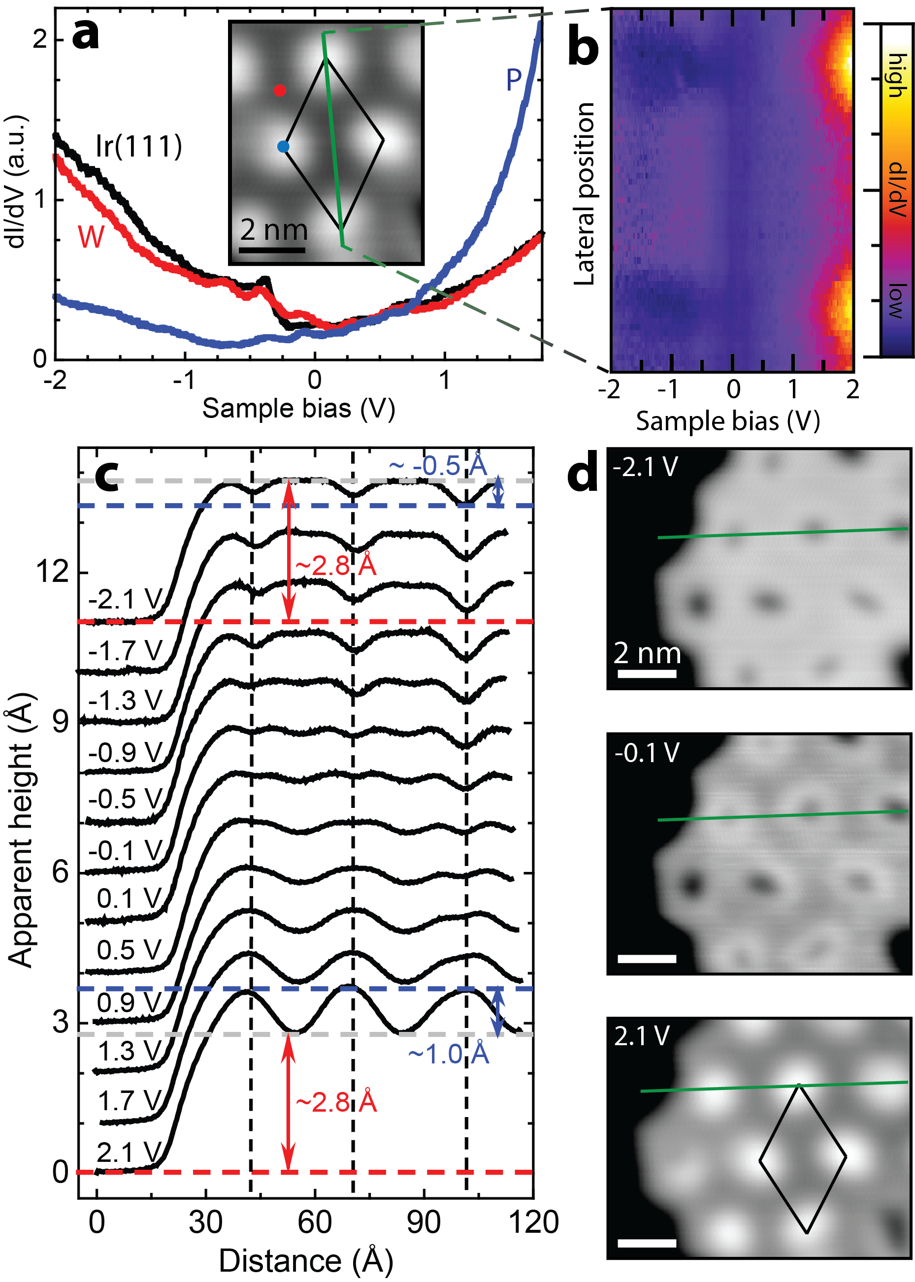
Figure 2a compares differential conductance (d/d) spectra measured on the bare Ir(111) and on the pore and wire regions of the h-BN moiré. The reference spectrum of the bare iridium shows a step-like increase in the conductivity at -380 mV due to the hole-like surface state present at the (111)-terminated Ir surface.Varykhalov2012 ; Altenburg2012 Metallic surface states are well-known to be very sensitive to any kind of adsorbates. Depending on the nature and the strength of the interaction between surface and adsorbate, the binding energy of the surface state can shift,Louie1978 ; Souk1985 ; Park2000 ; Hoevel2001 ; Forster2003 its onset can broaden,Park2000 and its intensity can be attenuatedJonker1981 ; Souk1985 ; Forster2003 ; Nicoara2006 or eventually be completely quenched.Eberhardt1983 ; Tzeng2000 ; Hoevel2001 ; Torrente2008 The d/d spectrum taken on the wire region of the h-BN moiré exhibits a step-like feature around -360 mV, which we assign to the surface state. The fact that the surface state survives underneath the wire region and does not shift significantly, confirms the weak interaction of this part of the moiré unit cell with the Ir(111) surface. We note, however, that the onset is broadened, suggesting a decreased lifetime of holes in the surface state.Kliewer2000 In contrast, the spectrum taken on the pore does not show any features related to the surface state. It thus appears to be quenched (or at least strongly shifted) by the stronger interaction of the h-BN layer with the metallic surface on the pore region of the moiré unit cell. Instead, we find a sharp rise in the d/d signal at positive bias, starting around 1 V. The evolution in differential conductance along the moiré unit cell is depicted in Figure 2b, where a series of individual d/d spectra is shown as a function of lateral position in a two-dimensional colour plot. The strong increase at positive bias is observed exclusively at the pore, thus its origin must lie in the interaction of the h-BN with the metal substrate.
The different features of the d/d spectra are also reflected in the STM image contrast. Figure 2c shows STM line profiles of the h-BN moiré extracted from images taken at different sample biases showing clean Ir(111) as well as an h-BN island. The series goes from -2.1 V to 2.1 V and the profile crosses two moiré unit cells, as indicated by the green lines in the STM images in Figure 2d. At negative bias, the pores appear as depressions with an apparent depth of 0.3 - 0.5 Å, in agreement with the actual topographic corrugation obtained from the DFT simulation (Figure 1d). However, at large positive bias the moiré contrast inverts and the pores appear as protrusions with an apparent height of up to 1 Å with respect to the wire region. This can be directly related to the increased DOS on the pore region at high bias as depicted in the spectra in Figure 2a and b. At low biases, a bright rim appears around the pores with an apparent height larger than the wire or the pore. Note that the apparent height of the wire region with respect to the clean Ir(111) does not show any significant change over the entire bias region, being around 2.8 Å. This is in rough agreement with the h-BN-Ir(111) distance on the wire given by DFT of 3.3 Å (Figure 1d).
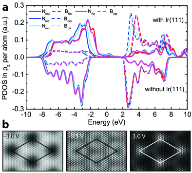
To further elucidate the origin of this contrast reversal, we have plotted in Figure 3a the projected density of the states (PDOS) of the orbital for boron and nitrogen atoms in the h-BN layer with (’positive’ PDOS) and without (’negative’ PDOS) the Ir(111) surface as obtained from our DFT calculations. The PDOS is split into different atomic registries with respect to the iridium surface, corresponding to different areas of the moiré unit cell. As expected, irrespective of the presence of the surface, the occupied states are dominated by the nitrogen atoms (full lines) and the unoccupied ones by the boron atoms (dashed lines). At the pore and at its rim, where the registries are BhcpNtop and BbriNtop, the entire PDOS is shifted to lower energies, i.e. the onset of the conduction band is observed at lower energies than at the wire region, causing the pores to appear bright at positive bias. As the valence band is shifted downwards as well, it becomes accessible only at larger negative bias compared to the wire, resulting in the pores being imaged as depressions and thus reversing the moiré STM contrast. Apart from the downward shift of the bands on the pore region, there is finite PDOS around the Fermi energy for the h-BN in Ir(111), indicating a partial - albeit small - hybridization of h-BN states with electronic states of the underlying metal substrate (most likely with the partially filled states of the iridium,Preo2007 ; Laskowski2008 ; Orlando2012 ) in agreement with previous experimental findings.Preo2007 Again, this effect is the strongest for the registries corresponding to the pore and rim regions of the moiré, in accordance with the increased interaction with the substrate. At small energies around zero, the rim and the pore show the largest DOS, which in conjunction with the actual topographic corrugation causes the rim to appear the brightest at small biases. We can reproduce the observed contrast changes by using our DFT results to simulate STM images, following the Tersoff-Hamann model.Tersoff1985 Figure 3b depicts a set of such simulations, for sample biases of , and V. The images at large negative and large positive bias yield excellent agreement with the experimental observations, as the appearance of the pore switches from a depression to a protrusion. Also the bright rim around the pore at low voltages is well reproduced by our STM simulation.
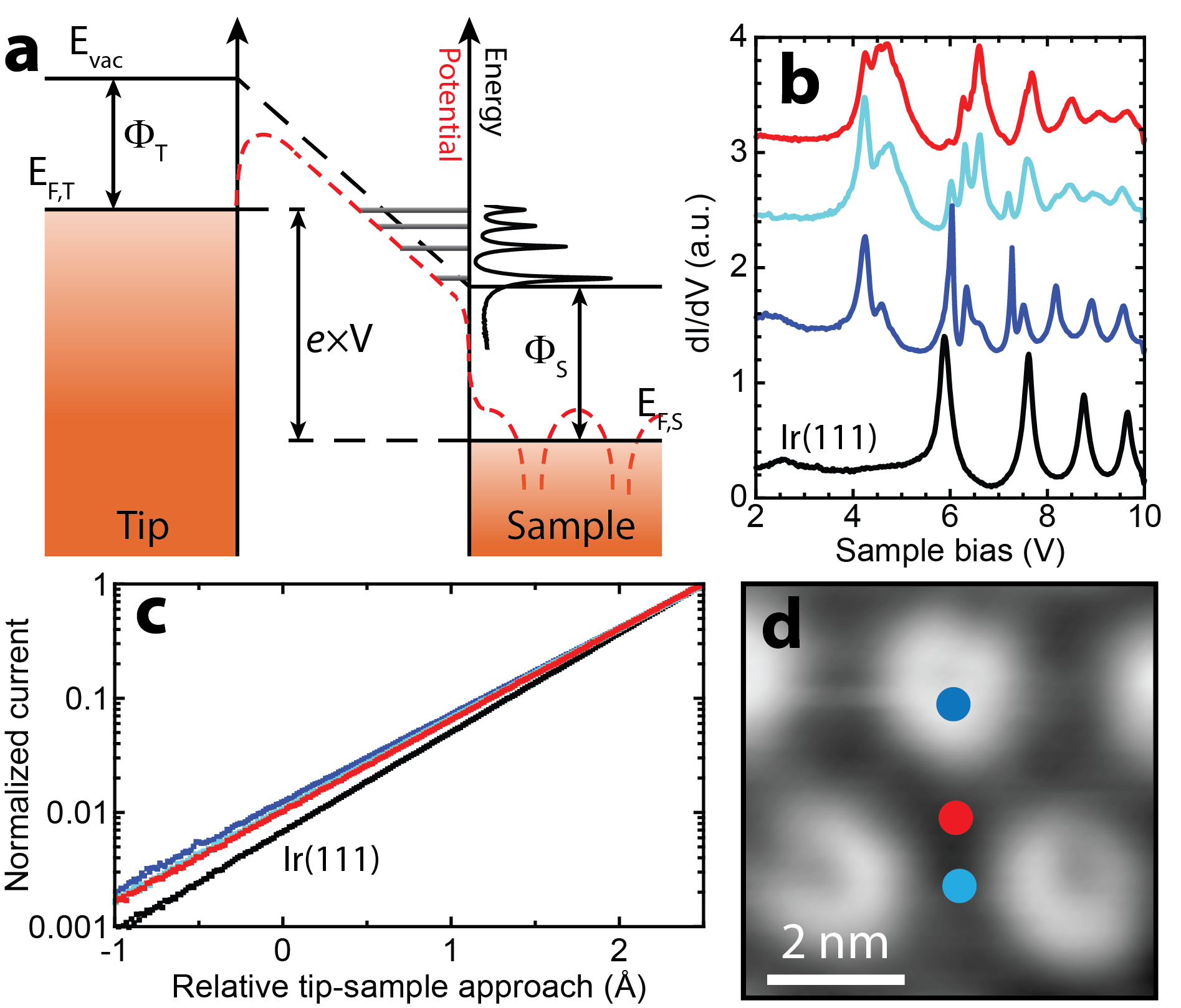
These variations in the electronic structure of the h-BN layer suggest a possible modification of the local tunneling barrier along the moiré unit cell. The tunneling barrier is directly related to the local work function or surface potential, which can be probed with high spatial resolution by measuring field emission resonances in the STM junction.Binnig1985 ; Becker1985 FERs, also known as Gundlach oscillations Gundlach1966 arise in the regime of Fowler-Nordheim tunneling,Fowler1928 i.e. when the applied bias is larger than the sample work function and thus, the tip Fermi level is above the vacuum level of the sample. The trapezoidal potential due to the drop of the bias voltage along the tunneling junction can give rise to hydrogen-like electronic resonances confined in the vacuum junction by the sample surface and the classical turning point at that trapezoidal potential, as depicted schematically in Figure 4a. Qualitatively, these resonances can be understood as image potential states under an external electric field. As the energy of these resonances depends on the local work function of the sample Koles2000 , FERs have found wide application in the STM community to map work function changes, in particular of thin films grown on metal substrates such as oxide films Rienks2005 ; Koenig2009 , thin insulating layers of NaCl Pivetta2005 ; Ploigt2007 and CuN Ruggiero2007 or monolayers of graphene Wang2010 and h-BN Joshi2012 . To a first approximation, the sample work function is given by the energy of the first FER. Figure 4b shows FER spectra measured at different parts of the h-BN moiré as well as on the clean Ir(111) for comparison.
On the bare iridium, the first FER appears at 5.8 V, in good agreement with the work function of Ir(111) of 5.76 eV.Michaelson1977 In contrast, the h-BN yields its first FER at 4.2 to 4.4 V, indicating a strong reduction of the work function on the h-BN overlayer of around 1.4 eV. This overall work function reduction is comparable with previously reported values for other h-BN/metal systems.Morscher2006 ; Goriachko2007 ; Joshi2012 Interestingly, the first three FERs of the h-BN layer show some internal structure, being actually composed of three subpeaks, whose relative intensities vary depending on the area within the moiré unit cell. Such an effect has been observed previously when measuring FERs over the moiré of one monolayer of FeO on Pt(111) and was attributed to contributions from different parts of the moiré unit cell.Rienks2005 It has been pointed out that since FERs are measured in a closed feedback configuration and at large bias (thus at a large tip-sample distance) the effective area that is probed can be in the order of 100 Å2.Becker1985 ; Rienks2005 The subpeaks are most clearly resolved in the second FER of the h-BN. In fact, it has been shown that the energetic position of the second FER is a good measure to determine relative shifts of the surface potential on the local scale, as it is less influenced by the image potential at the sample surface.Lin2007 Inspecting the internal structure of the second FER for the different parts of the h-BN moiré, we find the three peaks being located at 6.0, 6.3 and 6.6 V. The subpeak of lowest energy has its maximum intensity at the pore, while the peak of highest energy shows maximum intensity on the wire region, indicating a reduction of the work function when going from the wire to the pore. This result is supported by measurements of the local barrier heights using () spectroscopy. The tunneling current decreases exponentially with increasing tip-sample distance, whereby the decay constant is proportional to the square root of the apparent barrier height. Normalized spectra, taken on clean Ir(111) and on different parts of the h-BN moiré, are plotted in Figure 4c; it clearly can be seen that on both the pore and wire, the current decays much more slowly than on the clean iridium, indicating a lower apparent tunneling barrier. Approximating the barrier height as the average work function of the tip-sample system, i.e. ,Kern2010 we can deduce from an exponential fit and via Kern2010 an overall work function reduction w.r.t. the iridium surface of 1.6 eV for the wire and 1.2 eV for the pore (note that and refer to the potential barriers as determined from the exponential fit). Combining the results of the FER and measurements, we find a modulation of the work function within the moiré of roughly 0.5 eV.
For a more detailed mapping of the work function variations, we measured FER spectra along the high-symmetry line of the moiré unit cell connecting two next-nearest neighbor pores with each other (Figure 5a). The result is displayed as color-coded d/d intensity as a function of lateral position and applied sample bias in Figure 5b. At the pores, the second FER yields its highest intensity at 6.2 V, with little variation along the area of the pore. On the wire region, the maximum intensity is found between 6.6 and 6.7 V, with a slight asymmetry between the upper and lower part of the wire. Interestingly, the transition from low work function at the pore to high work function at the wire appears rather sudden, indicated by the co-existence region of the two corresponding peaks instead of a smooth shift of the second FER towards higher energy.
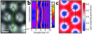
To compare the experimentally measured variations in the local surface potential with our DFT calculations, we have plotted the calculated Hartree potential above the h-BN layer in Figure 5c, which is approximately equal to the local work function. The simulation confirms that the pores of the h-BN moiré yield the lowest work function of 4.2 eV; the highest work function of 4.6 eV is found at the wire region that corresponds to the BfccNhcp registry, while the BtopNfcc wire region has a slightly lower work function. Thus, the variation of the work function follows the modulation in the interaction strength between the different regions of the h-BN moiré and the iridium substrate, allowing us to relate the observed changes to the calculated PDOS of the B and N orbitals. First, we note that the overall reduction of the work function - confirmed by our DFT calculations to be more than 1 eV - can be explained by the ‘push-back’ or ‘pillow’ effect:Ishii1999 ; Hwang2009 Due to the large spill-out of the electronic wave functions at a metal surface, an interface dipole-layer pointing into the vacuum is formed.Smoluchowski1941 This dipole-layer is known to have a significant contribution to the work function of metals (as it points towards the vacuum, it increases the magnitude of the work function).Smoluchowski1941 ; Lang1971 ; Nieminen1976 However, upon formation of the h-BN layer, the wave function spill-out is strongly reduced (‘push-back’) due to the Pauli exclusion principle, resulting in a reduction of the work function. Now, to explain the variations of the work function within the h-BN moiré unit cell, we recall that the PDOS plotted in Figure 3a indicates a hybridization of orbitals of the nitrogen atoms with states of the underlying metal substrate. This implies a re-distribution of electron density from the h-BN layer across the interface towards the metal substrate, i.e. the h-BN layer becomes slightly positively charged. As a result, an interface dipole pointing towards the metal substrate is formed and reduces the work function further. This hybridization effect is the strongest at the pore where N occupies top positions and the interaction between h-BN and Ir(111) is maximum, thus the work function is the lowest on the pore. On the wire, in particular on the least interacting regions where the registry is BfccNhcp and BtopNfcc, the hybridization is minimal and thus, this is the region with the largest work function within the moiré unit cell. Overall, the calculated work function yields very good agreement - qualitatively and quantitatively - with our FER measurements.
IV Conclusions
In summary, we have provided a detailed description of the structure of monolayer h-BN grown on Ir(111) at the atomic level. Due to the lattice mismatch between the h-BN and the Ir(111), a moiré superstructure with a periodicity of 29 Å and a corrugation of 0.4 Å is formed. The strongly interacting pores of the moiré corresponds to a BhcpNtop registry, while the regions on the wire with a BfccNhcp registry have the weakest interaction with the substrate. The orbitals of the nitrogen atoms partially hybridize with the metal substrate. As the magnitude of the hybridization depends on the interaction strength and thus on the atomic registry, it gives rise to a modulation of the work function within the moiré unit cell of 0.5 eV. Overall, the h-BN layer reduces the work function of the Ir(111) substrate by more than 1 eV. Our results are in line with previous findings that the strength of the chemical interaction at the interface of h-BN and Ir(111) should be less than for Rh(111) or Ru(0001) but more than for Pt(111).Preo2007 Therefore, the moiré pattern formed by h-BN/Ir(111) combines the advantages found in strongly interacting h-BN/metal system of large work function modulation and single domain growth with a low structural corrugation, the latter usually characteristic for weakly interacting h-BN/metal systems. This makes it a superior candidate for the bottom-up fabrication of electronically modulated thin films and hetero-sandwich structures.
Acknowledgements.
This research made use of the Aalto Nanomicroscopy Center (Aalto NMC) facilities and was supported by the European Research Council (ERC-2011-StG No. 278698 "PRECISE-NANO"), the Academy of Finland (Centre of Excellence in Low Temperature Quantum Phenomena and Devices No. 250280), and the Finnish Academy of Science and Letters.References
- (1) C. R. Dean, A. F. Young, I. Meric, C. Lee, L. Wang, S. Sorgenfrei, K. Watanabe, T. Taniguchi, P. Kim, K. L. Shepard, and J. Hone, Nat. Nanotechnol. 5, 722 (2010)
- (2) B. Hunt, J. D. Sanchez-Yamagishi, A. F. Young, M. Yankowitz, B. J. LeRoy, K. Watanabe, T. Taniguchi, P. Moon, M. Koshino, P. Jarillo-Herrero, and R. C. Ashoori, Science 340, 1427 (2013)
- (3) L. Liu, J. Park, D. A. Siegel, K. F. McCarty, K. W. Clark, W. Deng, L. Basile, J. C. Idrobo, A.-P. Li, and G. Gu, Science 343, 163 (2014)
- (4) M. Corso, W. Auwärter, M. Muntwiler, A. Tamai, T. Greber, and J. Osterwalder, Science 303, 217 (2004)
- (5) R. Laskowski, P. Blaha, T. Gallauner, and K. Schwarz, Phys. Rev. Lett. 98, 106802 (2007)
- (6) M. Corso, T. Greber, and J. Osterwalder, Surf. Sci. 577, L78 (2005)
- (7) A. Goriachko, Y. He, M. Knapp, H. Over, M. Corso, T. Brugger, S. Berner, J. Osterwalder, and T. Greber, Langmuir 23, 2928 (2007)
- (8) S. Berner, M. Corso, R. Widmer, O. Groening, R. Laskowski, P. Blaha, K. Schwarz, A. Goriachko, H. Over, S. Gsell, M. Schreck, H. Sachdev, T. Greber, and J. Osterwalder, Angew. Chem. Int. Ed. 46, 5115 (2007)
- (9) H. Dil, J. Lobo-Checa, R. Laskowski, P. Blaha, S. Berner, J. Osterwalder, and T. Greber, Science 319, 1824 (2008)
- (10) S. Kahle, Z. Deng, N. Malinowski, C. Tonnoir, A. Forment-Aliaga, N. Thontasen, G. Rinke, D. Le, V. Turkowski, T. S. Rahman, S. Rauschenbach, M. Ternes, and K. Kern, Nano Lett. 12, 518 (2012)
- (11) S. Joshi, D. Ecija, R. Koitz, M. Iannuzzi, A. P. Seitsonen, J. Hutter, H. Sachdev, S. Vijayaraghavan, F. Bischoff, K. Seufert, J. V. Barth, and W. Auwaerter, Nano Lett. 12, 5821 (2012)
- (12) F. Schulz, R. Drost, S. K. Hämäläinen, and P. Liljeroth, ACS Nano 7, 11121 (2013)
- (13) S. Joshi, F. Bischoff, R. Koitz, D. Ecija, K. Seufert, A. P. Seitsonen, J. Hutter, K. Diller, J. I. Urgel, H. Sachdev, J. V. Barth, and W. Auwärter, ACS Nano 8, 430 (2014)
- (14) A. Preobrajenski, A. Vinogradov, and N. Mårtensson, Surf. Sci. 582, 21 (2005)
- (15) S. Roth, F. Matsui, T. Greber, and J. Osterwalder, Nano Lett. 13, 2668 (2013)
- (16) A. B. Preobrajenski, M. A. Nesterov, M. L. Ng, A. S. Vinogradov, and N. Martensson, Chem. Phys. Lett. 446, 119 (2007)
- (17) F. Müller, K. Stöwe, and H. Sachdev, Chem. Mater. 17, 3464 (2005)
- (18) M. Morscher, M. Corso, T. Greber, and J. Osterwalder, Surf. Sci. 600, 3280 (2006)
- (19) F. Müller, S. Hüfner, H. Sachdev, R. Laskowski, P. Blaha, and K. Schwarz, Phys. Rev. B 82, 113406 (2010)
- (20) J. G. Diaz, Y. Ding, R. Koitz, A. P. Seitsonen, M. Iannuzzi, and J. Hutter, Theor. Chem. Acc. 132, 1350 (2013)
- (21) F. Orlando, R. Larciprete, P. Lacovig, I. Boscarato, A. Baraldi, and S. Lizzit, J. Phys. Chem. C 116, 157 (2012)
- (22) R. Laskowski, P. Blaha, and K. Schwarz, Phys. Rev. B 78, 045409 (2008)
- (23) J. Lu, P. S. E. Yeo, Y. Zheng, H. Xu, C. K. Gan, M. B. Sullivan, A. Castro Neto, and K. P. Loh, J. Am. Chem. Soc. 135, 2368 (2013)
- (24) I. Horcas, R. Fernandez, J. M. Gomez-Rodriguez, J. Colchero, J. Gomez-Herrero, and A. M. Baro, Rev. Sci. Instrum. 78, 013705 (2007)
- (25) M. Ruby, SpectraFox, http://www.spectrafox.com
- (26) J. VandeVondele, M. Krack, F. Mohamed, M. Parrinello, T. Chassaing, and J. Hutter, Comput. Phys. Commun. 167, 103 (2005)
- (27) J. VandeVondele and J. Hutter, J. Chem. Phys. 127, 114105 (2007)
- (28) Y. K. Zhang and W. T. Yang, Phys. Rev. Lett. 80, 890 (1998)
- (29) S. Grimme, J. Antony, S. Ehrlich, and H. Krieg, J. Chem. Phys. 132, 154104 (2010)
- (30) J. Tersoff and D. R. Hamann, Phys. Rev. B 31, 805 (1985)
- (31) J. Coraux, A. T. N‘Diaye, C. Busse, and T. Michely, Nano Letters 8, 565 (2008)
- (32) P. W. Sutter, J.-I. Flege, and E. A. Sutter, Nature Materials 7, 406 (2008)
- (33) H. P. Singh, Acta Crystallogr. Sect. A 24, 469 (1968)
- (34) R. S. Pease, Acta Crystallogr. 5, 356 (1952)
- (35) A. T. N’Diaye, J. Coraux, T. N. Plasa, C. Busse, and T. Michely, New J. Phys. 10, 043033 (2008)
- (36) N. Blanc, J. Coraux, C. Vo-Van, A. T. N’Diaye, O. Geaymond, and G. Renaud, Phys. Rev. B 86, 235439 (Dec 2012)
- (37) H. Hattab, A. T. N’Diaye, D. Wall, C. Klein, G. Jnawali, J. Coraux, C. Busse, R. van Gastel, B. Poelsema, T. Michely, F.-J. Meyer zu Heringdorf, and M. Horn-von Hoegen, Nano Lett. 12, 678 (2012)
- (38) S. K. Hämäläinen, M. P. Boneschanscher, P. H. Jacobse, I. Swart, K. Pussi, W. Moritz, J. Lahtinen, P. Liljeroth, and J. Sainio, Phys. Rev. B 88, 201406 (2013)
- (39) A. Varykhalov, D. Marchenko, M. R. Scholz, E. D. L. Rienks, T. K. Kim, G. Bihlmayer, J. Sánchez-Barriga, and O. Rader, Phys. Rev. Lett. 108, 066804 (2012)
- (40) S. J. Altenburg, J. Kröger, T. O. Wehling, B. Sachs, A. I. Lichtenstein, and R. Berndt, Phys. Rev. Lett. 108, 206805 (2012)
- (41) S. G. Louie, Phys. Rev. Lett. 40, 1525 (1978)
- (42) P. Soukiassian, R. Riwan, J. Lecante, E. Wimmer, S. R. Chubb, and A. J. Freeman, Phys. Rev. B 31, 4911 (1985)
- (43) J. Y. Park, U. D. Ham, S. J. Kahng, Y. Kuk, K. Miyake, K. Hata, and H. Shigekawa, Phys. Rev. B 62, 16341 (2000)
- (44) H. Hövel, B. Grimm, and B. Reihl, Surf. Sci. 477, 43 (2001)
- (45) F. Forster, G. Nicolay, F. Reinert, D. Ehm, S. Schmidt, and S. Hüfner, Surf. Sci. 532, 160 (2003)
- (46) B. T. Jonker, J. F. Morar, and R. L. Park, Phys. Rev. B 24, 2951 (1981)
- (47) N. Nicoara, E. Roman, J. M. Gomez-Rodriguez, J. A. Martin-Gago, and J. Mendez, Organic Electron. 7, 287 (2006)
- (48) W. Eberhardt, S. G. Louie, and E. W. Plummer, Phys. Rev. B 28, 465 (1983)
- (49) C. T. Tzeng, W. S. Lo, J. Y. Yuh, R. Y. Chu, and K. D. Tsuei, Phys. Rev. B 61, 2263 (2000)
- (50) N. Gonzalez-Lakunza, I. Fernandez-Torrente, K. J. Franke, N. Lorente, A. Arnau, and J. I. Pascual, Phys. Rev. Lett. 100, 156805 (2008)
- (51) J. Kliewer, R. Berndt, E. V. Chulkov, V. M. Silkin, P. M. Echenique, and S. Crampin, Science 288, 1399 (2000)
- (52) G. Binnig, K. H. Frank, H. Fuchs, N. Garcia, B. Reihl, H. Rohrer, F. Salvan, and A. R. Williams, Phys. Rev. Lett. 55, 991 (1985)
- (53) R. S. Becker, J. A. Golovchenko, and B. S. Swartzentruber, Phys. Rev. Lett. 55, 987 (1985)
- (54) K. H. Gundlach, Solid State Electron. 9, 949 (1966)
- (55) R. H. Fowler and L. Nordheim, Proc. R. Soc. A 119, 173 (1928)
- (56) O. Y. Kolesnychenko, Y. A. Kolesnichenko, O. Shklyarevskii, and H. van Kempen, Physica B 291, 246 (2000)
- (57) E. D. L. Rienks, N. Nilius, H. P. Rust, and H. J. Freund, Phys. Rev. B 71, 241404 (2005)
- (58) T. König, G. H. Simon, H. P. Rust, and M. Heyde, J. Phys. Chem. C 113, 11301 (2009)
- (59) M. Pivetta, F. Patthey, M. Stengel, A. Baldereschi, and W. D. Schneider, Phys. Rev. B 72, 115404 (2005)
- (60) H.-C. Ploigt, C. Brun, M. Pivetta, F. Patthey, and W.-D. Schneider, Phys. Rev. B 76, 195404 (2007)
- (61) C. D. Ruggiero, T. Choi, and J. A. Gupta, Appl. Phys. Lett. 91, 253106 (2007)
- (62) B. Wang, M. Caffio, C. Bromley, H. Fruechtl, and R. Schaub, ACS Nano 4, 5773 (2010)
- (63) H. B. Michaelson, J. Appl. Phys. 48, 4729 (1977)
- (64) C. L. Lin, S. M. Lu, W. B. Su, H. T. Shih, B. F. Wu, Y. D. Yao, C. S. Chang, and T. T. Tsong, Phys. Rev. Lett. 99, 216103 (2007)
- (65) L. Vitali, G. Levita, R. Ohmann, A. Comisso, A. De Vita, and K. Kern, Nat. Mater. 9, 320 (2010)
- (66) H. Ishii, K. Sugiyama, E. Ito, and K. Seki, Adv. Mater. 11, 605 (1999)
- (67) J. Hwang, A. Wan, and A. Kahn, Mater. Sci. Eng. R-Rep. 64, 1 (2009)
- (68) R. Smoluchowski, Phys. Rev. 60, 661 (1941)
- (69) N. D. Lang and W. Kohn, Phys. Rev. B 3, 1215 (1971)
- (70) R. M. Nieminen and C. H. Hodges, J. Phys. F 6, 573 (1976)