Enhanced persistent photoconductivity in -doped LaAlO3/SrTiO3 heterostructures
Abstract
We report the effect of -doping at LaAlO3/SrTiO3 interface with LaMnO3 monolayers on the photoconducting (PC) state. The PC is realized by exposing the samples to broad band optical radiation of a quartz lamp and 325 and 441 nm lines of a He-Cd laser. Along with the significant modification in electrical transport which drives the pure LaAlO3/SrTiO3 interface from metal-to-insulator with increasing LaMnO3 sub-monolayer thickness, we also observe an enhancement in the photo-response and relaxation time constant. Possible scenario for the PC based on defect-clusters, random potential fluctuations and large lattice relaxation models have been discussed. For pure LaAlO3/SrTiO3, the photoconductivity appears to originate from inter-band transitions between Ti-derived bands which are in character and O 2p - Ti hybridized bands. The band structure changes significantly when fractional layers of LaMnO3 are introduced. Here the Mn bands ( eV above the Fermi energy) within the photo-conducting gap lead to a reduction in the photo-excitation energy and a gain in overall photoconductivity.
I introduction
The origin of the two-dimensional electron gas (2DEG) at the interface of artificially tailored oxide heterostructures Muller ; Ohtomo ; Hwang ; Caviglia ; Thiel is attributed to both intrinsic and extrinsic factors. While the former is accounted for the polar catastrophe model, Huijben ; Millis extrinsic factors are associated with defects, such as oxygen vacancies Siemons ; Kalabukhov ; Herranz1 and inter-site cation mixing Tokura ; Pulikkotil that are introduced in the system during film growth. Huijben1 ; Herranz The latter argument is substantiated by the observation of a clear dependence of the interface conductivity on pressure during the film growth. Huijben ; Herranz Furthermore, the observation of persistent photo-conductivity (PPC) with large relaxation time also points to the role of defect induced states in these oxide heterostructures. Rastogi ; Rastogi01 ; Rastogi02 However, there also exists conclusive evidence that defects in the form of O-vacancies in the SrTiO3 substrate are not the only responsible factor that leads to 2DEG at the interface. Had so been the case, then irrespective of the nature of the films, a 2DEG would have been observed for most of the perovskite oxides deposited on SrTiO3, including for LaCrO3 and LaMnO3. Beyond, we note that doping induces electronic phase transition and metallicity in both LaCrO3 and LaMnO3.Sakai ; Schiffer ; Park On the other hand, transport measurements find that the LaCrO3 and LaMnO3 films deposited on TiO2 terminated SrTiO3 substrate results in no 2DEG at the interface, irrespective of the film thickness and deposition conditions. Chambers01 ; Barriocanal
In general, a 2DEG state is observed at the interface of a non-polar (TiO2 terminated SrTiO3) and a polar material (such as LaAlO3) motif. Under these circumstances, the in-built electric field at the interface causes bending of conduction and valence band edges of SrTiO3, leading to a triangular potential well which is filled by electrons transferred from the LaAlO3 over-layers. Nakagawa ; Stengel ; Pentcheva ; Chen ; Son ; Ramesh Although, this model explains many of the experimental observations, it fails to account for the observed charge carrier density that has its dependence on the thickness of the deposited LaAlO3 film. Thiel ; Caviglia Beyond, the model also has little support from the photo-emission spectroscopy studies. Segal ; Chambers ; Janicka ; Yoshimatsu
A fundamental understanding of the underlying mechanism for the formation of the 2DEG therefore requires use of perturbative techniques, which will lead to injection of additional charge carriers at the interface and selective and controlled modification of the interface chemistry. While the former is realized by electrostatic gating and photo-excitation, Thiel ; Rastogi ; Rastogi02 the latter can be achieved by - doping at the interface, a concept commonly used in III-V compound semiconductor quantum wells. Tusi
The effect of electrostatic gating of LaAlO3/SrTiO3 interface has been studied extensively. The gate field either draws charges towards the interface from the over-layers or pushes charge towards it resulting in a gate controlled metal-insulator phase transition. Thiel ; Caviglia01 It has also been shown earlier that the electronic transport in oxide heterostructures can be altered significantly on exposure to electromagnetic radiation of optical frequency making these potential candidates in opto-electronic applications. Rastogi01 ; Rastogi02 ; Rastogi For the conducting interface of LaTiO3/SrTiO3 and LaAlO3/SrTiO3, the PPC is seen in the spectral range of 300 400 nm. It is also noticed that the magnitude and relaxation dynamics of the photo-conducting state depends on the growth temperature of LaTiO3 and LaAlO3, but is independent of the number of the film overlayers, since the response is only energetically close to the band gap of SrTiO3. It has been previously shown that SrTiO3 (single crystal and thin films) displays wide range of properties such as ferroelectric, Ishikawa ; Tikhomirov persistence photoconductivity Feng etc. Therefore, it is quite evident that the SrTiO3 substrate plays a crucial role in determining the electronic and optical properties in these heterostructures. The PPC seen in oxide interfaces is quite similar to that reported in the III-V semiconductor heterostructures. Arslan ; Stormer In analogy with the latter systems, the slow decay of the photo-current in oxides can be associated with the defect induced states in the SrTiO3 substrate. The longer life-time of the photo-induced carriers is largely attributed to the less dispersive Ti bands, which make up the conduction band Rastogi02 in these systems.
We have observed a systematic metal-to-insulator transition in LaAlO3/SrTiO3 system by controlled -doping at the interface with LaMnO3 monolayers. Rastogi03 Our present experiment rules out the possibility of interfacial intermixing as the cause of metallic conduction in LaAlO3/SrTiO3 system, because such a reaction of La/Sr at the interface would lead to formation of La1-xSrxTiO3 which should be conducting based on the simple valence argument. Our experiment also rules out the reduction of SrTiO3 as the cause of 2DEG, as reduction would take place even in the case of -LaMnO3 monolayer deposition, resulting in interfacial conductivity irrespective of the Mn concentration at the interface. While the present experiment validates the polarization catastrophe argument for the 2DEG formation, it remains to be seen what would happen to photo-conductivity when transfer of electrons from LaAlO3 overlayers are inhibited by the -LaMnO3 monolayer.
Here we present the results of photo-conductivity measurements on the -doped LaAlO3/SrTiO3 heterostructures, and compared them with the photo-response of the undoped LaAlO3/SrTiO3 system. The -doping is accomplished by means of a selective deposition of fractional monolayers of LaMnO3 on the TiO2 terminated SrTiO3 surface, followed by layer-by-layer growth of the LaAlO3 over the LaMnO3 layer. It has been shown previously that LaMnO3 films on SrTiO3 remain non-conducting irrespective of their thickness. Barriocanal Therefore, a controlled deposition of Mn ions at the LaAlO3/SrTiO3 interface is expected to provide a method to control the electronic phases and phase transition. In accordance, we find that the resistivity of the -doped LaAlO3/SrTiO3 increases non-trivially as the -LaMnO3 monolayer at the interface is thickened. Beyond, the results of photo-conductivity measurements reported here also include the following: (i) A larger photo-response with increasing -doped LaMnO3 interfacial layer thickness and, (ii) persistent photo-conductivity following a stretched exponential behavior with its decay constant increasing in proportion with the LaMnO3 monolayer thickness. Explanation to these results are sought in terms of a few well established models and also partly from the band structure calculations.
II Experimental details
The samples were grown by Pulsed Laser Deposition at 800oC and the thickness of LaAlO3 deposited on TiO2 terminated () SrTiO3 was kept at 20 unit-cell (uc). The deposition procedure, conditions and growth parameters are described in our earlier reports. Rastogi01 ; Rastogi02 ; Rastogi03 The -doping of the interface has been achieved by controlled growth ( - nm/s) of a LaMnO3 sub-monolayer prior to commencing deposition of LaAlO3 film. In its bulk form, LaMnO3 is a strongly correlated anti-ferromagnetic insulator. A schematic of the interfacial -doping with LaMnO3 is shown in the inset of Fig.1. To perform the transport measurements, Ag/Cr electrodes were deposited on the films (drain and source) and back of the substrate (gate) by thermal evaporation using shadow masks. Linear current versus voltage characteristics between drain and source confirm the Ohmic behavior of the electrodes, while the leakage current between the gate and source was less than nA. The photo-excitation experiments were carried out in a closed cycle helium optical cryostat where the samples were exposed to the broad band radiation of a Xenon lamp, whose spectrum contains % of UV radiation, and two single wavelength (441 and 325 nm) lines of a He-Cd laser through a quartz window.
III Results
III.1 Electrical Resistivity
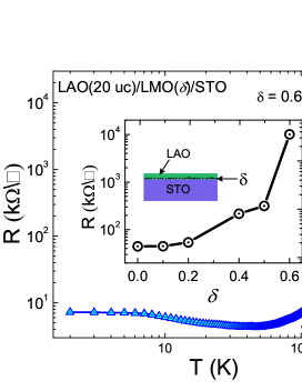
The temperature dependence of the sheet resistance () of the LaAlO3/SrTiO3 and that of the -LaMnO3 doped samples is shown in Fig.1. Consistent with the previous reports, a unit cell thick LaAlO3 film on TiO2 terminated SrTiO3 substrate showed metallic characteristics. Rastogi01 ; Rastogi02 ; Rastogi03 However, on embedding LaMnO3 sub-monolayer at the interface, we observe a systematic transition to insulating state. We have also noticed that the critical thickness of the LaAlO3 over-layer required to induce 2DEG in -LaMnO3 doped heterostructures is proportional to the sub-monolayer thickness of the -LaMnO3. Rastogi03 This study also revealed that uc thick LaMnO3 drives the interface to insulating state when the LaAlO3 overlayer thickness was of 20 uc. We note that the critical thickness of LaMnO3 to make the interface insulating is much smaller when LaAlO3 layer is only 10 uc. The plot of (T) for -doped LaMnO3 with sub-monolayer thickness is shown in Fig.1 along with (T) of undoped LaAlO3/SrTiO3.
III.2 Photo-response
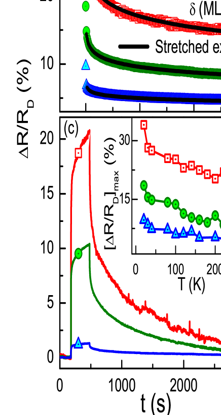
Fig. 2(a) shows the time evolution of resistance of three samples with and ML during the period when sample was exposed to the light and then allowed to recover in dark at 20 K. To better understand the recovery process, we have defined a normalized resistance R/RD, where R = R(t)-RD with R(t) being the resistance at time t and RD the resistance in dark. The details of these measurement have been described in an earlier report. Rastogi02 Fig. 2(b c) reveal that the relative change in the resistance on photo-exposure increases with -LaMnO3 layer thickness, while the recovery process slows down. It is important to point out here that the most change in the resistance on photo-exposure is triggered by the ultra-violet (UV) component of the quartz halogen lamp radiation. This fact is further established when we expose the sample to a monochromatic radiations ( = 325 and 441 nm) of He-Cd laser. These results are shown in the inset of Fig. 2(b), from which we find that relative change in the resistance of all heterostructures under consideration is significantly suppressed for 441 nm radiation, in comparison to that observed under the 325 nm radiation. In Table 1, we list the values of R/RD for all three samples achieved under 325 nm, 441 nm and xenon lamp radiation. The comparative study as highlighted in Table 1 shows that the overall photo-response increases with increasing doping of LaMnO3 at the interface. Also, our data suggests that the threshold wavelength to induce photo-conductivity in these heterostructures shift towards higher wavelengths with doping. This effect has been qualitatively understood by means of band structure calculations, which is discussed in the next section.
| = 0 | = 0.2 | = 0.5 | |
|---|---|---|---|
| (R/RD)325nm | 0.0446 | 0.2236 | 0.3156 |
| (R/RD)441nm | 0.0094 | 0.0258 | 0.0481 |
| (R/RD)Broadband | 0.0187 | 0.1079 | 0.2089 |
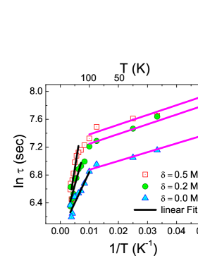
In Fig. 2(c) we show the R/RD data taken at 300 K and the temperature dependence of maximum R/RD (just after closing the shutter). The response decreases monotonically with increasing temperature and it is higher in -doped samples. In general, the recovery to the resistive state on shutting off the light is well described by a stretched exponential of the form R with , and, being the relaxation time constant. A fit (shown by the solid lines in Fig. 2(b)) yields varying from to seconds as the thickness of the -layer is increased to uc. Correspondingly, the exponent goes from to . Further, the recovery dynamics depend strongly on temperature. In order to understand the recovery process and the mechanisms involved, we fit the data to Arrhenius equation given as = , where and are the activation energy for detrapping the photo-generated carriers and Boltzmann constant, respectively. The plots of against are shown in Fig.3. Clearly, two distinct temperature regions of activation can be seen in the Arrhenius plot. At low temperatures T K, the calculated value of is in the range meV, for all samples. However, at higher temperatures, the for uc thick LaMnO3 is estimated as meV, which is almost three times higher in comparison to the activation energy of LaAlO3/SrTiO3 system ( meV).
A sudden change in the slope about K is observed in Arrhenous plot (Fig. 3). This temperature is very close to the structural phase transition of SrTiO3 ( K). We believe that such a phase transition would be of lesser significance, as the cubic to tetragonal transition of SrTiO3 is partly due to its latent paraelectric nature, which is intimately associated with the d0-ness of the Ti ions in SrTiO3. In this case, the interface modifies the occupation of Ti with extra electrons being doped and therefore such a transition is not expected in the SrTiO3 motif near to the interface, although one may expect the same to happen deep down in the substrate.
The electrical conductivity of these structures undergoes strong modulation when a gate field is applied. It has been shown earlier that the electrostatic and photon fields act on two different sets of charge carriers. Rastogi02 While the recovery time from the photo-illuminated state stretches over several hours, the system was found to recover to the unperturbed normal state with in microseconds after switching off the gate field. Hence, the role of -layer influencing the migration of these two sets of carriers needs to be examined. We have studied the influence of electric field perturbation on the photo-induced relaxation processes of the -doped LaMnO3 interfaces in comparison with that of the pure LaAlO3/SrTiO3 system.
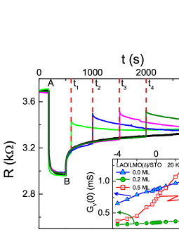
In Fig.4 we illustrate our measurement scheme to study the effects of a gate electric field on the recovery process. At point ‘A’ of the plot in Fig. 4 the sample is exposed to light, which triggers a sharp drop in resistance followed by saturation. At point ‘B’ the illumination is turned off and the recovery dynamics thereafter is examined by applying a gate field (Eg) of kV/cm after a certain time gap, which has been changed from t1 to t4 in four sets of exposure-recovery experiments. We find that the resistance changes spontaneously on gating. While positive Eg enhances the channel conductivity, negative Eg tend to reduce it. For better understanding of the effect of gate field alone, we have measured source to drain I-V characteristic of these samples under different gate fields. The slope of these linear curves at the origin gives the zero-bias conductance GV(0) which is plotted in the inset of Fig. 4. We observe an order in magnitude decreased in the GV(), in the ML sample.
III.3 Electronic structure
The threshold energy required to impart photo-conductivity in LaAlO3/SrTiO3 corresponds to that of near ultra-violet wavelength. Numerical calculations based on density functional theory are consistent with this picture. Rastogi02 The optical transitions are associated to those states which are in the range eV above and below the Fermi energy, thereby providing the estimate of photo-conducting threshold wavelength as nm.
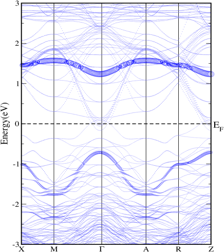
However, the photo-response of the -doped LaAlO3/SrTiO3 heterostructures show subtle signatures of the photo-response threshold shifting to lower photon energy, which suggests a modification in the band structure caused by the Mn ions in the vicinity of the interface. In Fig.5, we show the band structure of the -doped LaAlO3/SrTiO3. A fully relaxed super-cell of 229 dimension with unit-cells of SrTiO3 as substrate with TiO2 termination is modeled in the present study. The -doping with ML thick LaMnO3 is modeled by Mn-Al chemical disorder near to the interface. The Brillouin zone integration were carried out on a space grid with the WIEN2K Blaha parameters and to be as and , respectively. The numerical details of the structure optimization, self-consistent total energy and that of the electronic structure are similar to those described in Ref. 17. Both in local density approximation (LDA) and generalized gradient approximation (GGA), Mn ions modeled at the interface of LaAlO3/SrTiO3 system yield a metallic state, with relatively high density of states, with the prominent states being the Mn states. It is well known that such spurious states at the Fermi energy are due consequence of the missing Coulomb correlation term in the Hamiltonian. In the present case, the Coulomb correlation effects (Ueff) of the Mn electrons are taken into consideration by the LDA+Ueff Hamiltonian, with Ueff= eV.
Before we discuss the band structure of the -doped LaMnO3, recall from Fig. of Ref. 17 that the calculated optical conductivity of the LaAlO3/SrTiO3 heterostructure matches well with that of the experiments. The consistency indicates the reliability of the band structure generated in the density functional theoretical formalism. The upper valence band of the LaAlO3/SrTiO3 system are primarily composed of O states of the AlO2 layers of the LaAlO3 film. Electronic states, eV below the Fermi energy, are the O states of the TiO2 layers of the substrate. On the other hand, the states above Fermi energy are primarily composed of Ti orbitals. At energies 2 eV above Fermi energy, one finds a bunching of Ti bands of primarily of the character. These states are relatively localized over a very narrow energy interval. Thus, photo-conductivity in LaAlO3/SrTiO3 heterostructures results from the inter-band transitions between Ti derived bands and that of the O - Ti amalgamation at the Fermi energy.
In case of -doped LaAlO3/SrTiO3 with LaMnO3 monolayers, the band structure as shown in Fig.5 shows localized Mn states (eg states) positioned eV above Fermi energy. The corresponding Mn states () in the valence band are relatively more dispersed over a wider energy range. Thus, it is evident that the positioning of the Mn states within the photo-conducting gap leads to a decrease in the photo-excitation energy, and therefore is expected to increase the overall photo-response. Thus, for small wavelength induced excitations one find the transition to occur between the states that lie between eV of the Fermi energy, while the small photo-generation of carriers at the nm is associated with the Ti states near the Fermi energy and the Mn bands which are relatively eV above the Fermi energy.
The computed band structure also qualitatively explains the relatively slow relaxation of the photo-generated carriers to the normal state in the -doped systems with that of the pure LaAlO3/SrTiO3. The energy-time relation of the uncertainty principle suggests that the life-time of photo-generated carriers in a given band would be inversely proportional to the energy band width. Along these perspectives, finding that the Mn bands which are highly localized and positioned at eV above the Fermi energy would serve as localized traps for the photo-induced charge carriers, thereby increasing the relaxation time in -doped systems in comparison with the parent system.
IV Discussion
For abrupt interfaces of oxide heterostructures, the polar catastrophe model is quite robust to account for the origin of 2DEG. The model asserts on band bending effects via electronic reconstruction due to the in-built electric field at the interface of the polar (LaAlO3)nonpolar (SrTiO3) materials. PPC in these systems can therefore be related to the model proposed by Queisser and Theodorou (QT), where its emergence is associated with the macroscopic potential barriers induced by the band bending effects. Queisser Such potential barriers lead to the PPC effect by spatial separation of the photo-generated electrons and holes. With one type of carrier being trapped, the other remains free and causes excess conductivity. Lee The model can be verified by studying the excitation-energy dependence of PPC. For this we used the two excitation energies afforded from He-Cd laser, which gives one of the excitation energy (2.8 eV) less while the other one larger (3.8 eV) than the band gap energy of SrTiO3. The results are displayed in Table- 1 and inset of Fig. 2(b). For pure LaAlO3/SrTiO3 heterostructures, we observed very small change in the resistance and also weak signature of PPC with the photo-excitation below the absorption edge, while for -doped samples a large PPC effect could be seen, which increases monotonically with the -layer thickness. These results infer that the PPC of undoped sample have little contribution arising from spatial separation of the photo-generated carries, primarily due to the band bending effects. While in the case of -doped systems, this effect seems to be less prominent. The change in the resistance of -doped systems with lower excitation can be attributed to the finite absorption of incident illumination by in-gap states present in the SrTiO3 band gap and reduce the possibility of band bending scenario. It has also been shown the 2DEG confinement can be explained by the formation of metal induced gap states in the band gap of SrTiO3 rather than the band bending Janicka and no measurable band bending is observed in La1-xAl1+xO3/SrTiO3(001) hetero-junctions. Qiao Thus, the model based on the spatial separation of the photoexcited electrons and holes by macroscopic potential barrier due to band bending looks less appropriate to account for the PPC here. However, if the band bending is due to the O-vacancies, then the associated barrier would spatially separate the electrons that constitute the 2DEG. Although, this can lead to some justification of the QT model to the observed PPC effects in the present hetero-structured systems, the observed decay kinetics does not seem to support the model as a predominant process for inducing PPC. The above picture of band bending is further established by the analysis of the PPC decay dynamics as proposed in QT model for artificially tailored heterostructures. Queisser We tried to fit the decay to a logarithmic behavior of the form, , where a and b are constants, with respect to time. We find that the logarithmic fit becomes poorer and deviates significantly from the measured data as the -layer thickness is increased. However, the undoped system still displays a better tolerance to the fit and low residual values as compared to the -doped samples, which strengthen our argument.
Various other models have also been proposed to account for the PPC effects in solid state materials. Lang ; Queisser ; Mooney ; Jiang ; Iseler ; Schubert Earliest of all was associated to inhomogeneities in the samples, caused either by bonding configurations, spatial variation in the chemical composition and/or in local charge densities. A much more advanced model was due to Theodorou and Symeonides, Theodorou who proposed the role of defect clusters in the sample. Such defects may be inevitable and are generally introduced during the growth itself. On preliminary grounds, the defect-cluster model may look appropriate to account for PPC in these heterostructures, as the synthesis technique employed in depositing -doped LaAlO3 films on SrTiO3 substrates are by means of the laser ablation. This highly energetic deposition process could result in clusterization of the Mn and Al ions forming a disordered LaAl1-xMnxO3 monolayer. In cases where the local inhomogeneities lead to a density of the defects which is larger than the carrier density, a macroscopic potential barrier may be formed. Such defect-clusters may host traps, and upon electron capture would become charged. In turn, this would induce a charge of opposite polarity around the cluster, thus spatially separating the electron-holes pairs, impeding their recombination and resulting in PPC. Theodorou ; Theodorou1 However, the defect-cluster model predicts larger PPC in proportion to the thickness of the conducting layer. The latter, however, is in contrast with our observation in -doped LaMnO3 in the LaAlO3/SrTiO3 interface. We find that as the -doped sub-monolayer thickness is increased (larger Al/Mn disorder), the 2DEG conductivity decreases, but with an enhancement in the PPC. Thus, the defect-cluster model also seems less appropriate to account for the larger PPC seen in the -doped LaMnO3 in the samples.
A relevant model that appears to describe the PPC in the present case is based on potential fluctuations in the material. Permogorov ; Cohen ; Jiang ; Jiang1 ; Jiang2 ; Lin Here the spatial separation between photo-excited charge carriers by random local-potential fluctuations induced by compositional variations is held responsible for PPC. Jiang Within the framework of the polar catastrophe model, the origin of 2DEG is due to electronic reconstruction of the Ti ions at the interface. Thus, the 2DEG wave-function would be thought as a composition of Ti3+ and Ti4+ states. Moreover, the Mn ions in the monolayer would also exhibit multiple valence states. Certainly therefore, an energy barrier emanating from such a charge fluctuation would also act as a source of potential fluctuations. Besides, there is also a likelihood of chemical disorder due to random distribution of Al and Mn ions in the delta doped layer. Therefore, both chemical and valence state disorder can induce an uneven potential landscape at the interface of LaAlO3/SrTiO3 with -doping of the interface. However, this model predicts PPC to be observed at high temperatures, with a well defined transition temperature, which is in contrast with our observations, where enhanced PPC in seen at lower temperatures. But, we note that the decay kinetics predicted by the random potential fluctuation model is similar to that of a stretched exponential function.
The lattice relaxation model Lang ; Lang1 ; Zhou is one of the most widely accepted description for the PPC effects in semiconductor heterostructures. The model stipulates photo-excitation of carriers from defect induced deep-level traps . A barrier is created by lattice relaxation thereby preventing the recapture of mobile carriers. The source of the lattice relaxation could be ionic mismatch and/or vacancies. However, in the present context, mismatch in the lattice constants and/or that in the constituents ionic-radii, does not seems to be relevant. Therefore, the structural relaxation would be mainly due to oxygen vacancies, and hence these defects render a negative-U center. At low temperatures, thermal energy is not sufficient enough to overcome the barrier, and thus the photo-generated carriers remain in these shallow states, resulting in PPC. The PPC buildup and decay kinetics, in general, fit to a stretched exponential curve, which is similar to our observations for the oxide heterostructures. Rastogi01 ; Rastogi02 Due to the inherent propensity of LaMnO3 to attract oxygen, its presence in the vicinity of the interface can induce more vacancies in the substrate leading to a non-equilibrium chemical configuration. Thus, while the photo-ionization of oxygen specific defects in the quantum well region appears to be the dominant mechanism for PPC in oxide heterostructures, one cannot rule out the contribution of the spatially separated charges across the interface facilitated by the factors that have been mentioned above.
Moreover, as both Mn and Al occupy the substitutional body-centered site of the perovskite structure, the role of Mn ions on the lattice can also be partly inferred from the PPC data. It has been argued in the case of III-V and II-IV semiconductor heterostructures, and also in oxide heterostructures that the 2DEG at the interface is derived out of lattice strain. Within the realms of alloy theory, the solubility of Mn ions in LaAlO3 matrix, infers to a lowering of lattice strain . In general, reduction of strain decrease the activation energy with Mn at% in the monolayer, which, however, is in contradiction with our observation. Thus, the increase in activation energy with -doping at the interface may be attributed to the enhanced electron-electron interaction between the electrons in the trap and the unpaired electrons of the Mn ion. Such an event lead to a narrowing of the optical trap potential, which would narrow with increasing Mn at% at the interface, leading to a higher repulsive barrier for the electrons to return to the oxygen mediated defect centers, after photo-ionization. However, we note that there does not exist to the best of our knowledge, a scheme to estimate the strength of Coulomb scattering from the presence of the deep traps in the quantum well and its effect on transport properties. However, it is reported that in ZnSe/(Zn,Cd,Mn)Se heterostructured systems, the 2DEG exhibits a strong PPC that becomes more pronounced when the Mn2+ concentration is increased. Ray The enhanced PPC in this system is also accompanied by a decrease in sample mobility, suggesting a connection between the deep traps introduced by the magnetic Mn ions and enhanced Coulomb scattering.
V conclusion
In summary, we have investigated the effect of -doping on the photo-response of LaAlO3/SrTiO3 interfaces. The photo-response of the pure LaAlO3/SrTiO3 heterostructure is found to be sensitive to near ultra-violet radiation which shifts towards the lower photon energy upon doping the interface with LaMnO3. The doped samples show relatively large photo-response and time constant of recovery in comparison to the undoped sample. Based on theoretical calculations, we establish that the slow relaxation arises due to localized Mn states (3) which are situated 1.5 eV above the Fermi level. The positioning of these Mn bands within the photo-conducting gap shifts the photo-response threshold to higher photon wavelengths with increasing -doping in the heterostructures. We also have made an attempt to understand the decay dynamics of the photo-conducting state . Our experimental findings demonstrate that the defect-cluster and random fluctuation models are less appropriate to describe the large photo-response and high values of activation energies for the recovery seen in -doped samples. On other hand, the lattice relaxation model is found to be in better agreement. Moreover, our arguments also suggest that the increase in the activation energy could be attributed to the strong electron-electron interaction of the Mn-ions in the -doped monolayer at the interface.
Acknowledgements.
The authors gratefully acknowledge discussions with S. Auluck. A.R. would like to acknowledge the Council of Scientific and Industrial Research (CSIR), India and Indian Institute of Technology Kanpur for financial support. R.C.B. acknowledges financial support from J. C. Bose National Fellowship of the Department of Science and Technology, Government of India.References
- (1) A. Ohtomo, A. D. Muller, J. L. Grazul, and H.Y. Hwang, Nature (London) 419, 378 (2002).
- (2) A. Ohtomo and H. Y. Hwang, Nature 427, 423 (2004).
- (3) A. Ohtomo and H. Y. Hwang, Nature 441, 120 (2006).
- (4) S. Thiel, G. Hammer, A. Schmehl, C. W. Schneider, J. Mannhart, Science 313, 1942 (2006).
- (5) A. D. Caviglia, S. Gariglio, C. Cancellieri, B. Sacépé, A. Fête, N. Reyren, M. Gabay, A. F. Morpurgo, and J.-M. Triscone, Phys. Rev. Lett. 105,236802 (2010).
- (6) M. Huijben, G. Rijnders, D. H. A. Blank, S. Bals, S. Van Aert, J. Verbeeck, G. Van Tendeloo, A. Brinkman and H. Hilgenkamp, Nature Mater. 5, 556 (2006).
- (7) S. Okamoto, and A. J. Millis, Nature 428, 630 (2004).
- (8) W. Siemons, G. Koster, H. Yamamoto, W. A. Harrison, G.Lucovsky, T. H. Geballe, D. H. A. Blank, and M. R. Beasley, Phys. Rev. Lett. 98, 196802 (2007).
- (9) A. Kalabukhov, R. Gunnarsson, J. Börjesson, E. Olsson, T. Claeson, and D. Winkler, Phys. Rev. B 75, 121404 (2007).
- (10) G. Herranz, M. Basleticacute, M. Bibes, et al., Phys. Rev. Lett. 98, 216803 (2007).
- (11) Y. Tokura, Y. Taguchi, Y. Okada, Y. Fujishima, T. Arima, K. Kumagai, and Y. Iye, Phys. Rev. Lett. 70, 2126 (1993).
- (12) J. J. Pulikkotil, S. Auluck, P. Kumar, A. Dogra, and R. C. Budhani, Appl. Phys. Lett. 99, 081915 (2011).
- (13) M. Huijben, A. Brinkman, G. Koster, and G. Rijnders, H. Hilgenkamp, D. H. A. Blank, Adv. Mater. 21, 1665 (2009).
- (14) G. Herranz, M. Basletić, O. Copie, and M. Bibes, A. N. Khodan, C. Carrétéro, E. Tafra, E. Jacquet, K. Bouzehouane, A. Hamzić, and A. Barthélémy, Appl. Phys. Lett. 94, 012113 (2009).
- (15) A. Rastogi, A. K. Kushwaha, T. Shiyani, A. Gangawar, and R. C. Budhani, Adv. Mater. 22, 4448 (2010).
- (16) A. Rastogi and R. C. Budhani, Opt. Lett. 37, 317 (2012).
- (17) A. Rastogi, J. J. Pulikkotil, S. Auluck, Z. Hossain, and R. C. Budhani, Phys. Rev. B 86, 075127 (2012).
- (18) N. Sakai, H. Fjellvåg, and B. C. Hauback, J. Solid State Chem. 121, 202 (1996).
- (19) P. Schiffer, A. P. Ramirez, W. Bao, and S-W. Cheong, Phys. Rev. Lett. 75, 3336 (1995).
- (20) J.-H. Park, E. Vescovo, H.-J. Kim, C. Kwon, R. Ramesh and T. Venkatesan, Nature 392, 794 (1998).
- (21) S. A. Chambers, L. Qiao, T. C. Droubay, T. C. Kaspar, B.W. Arey, and P. V. Sushko Phys. Rev. Lett. 107,206802 (2011).
- (22) J. Garcia-Barriocanal, F. Y. Bruno, A. Rivera-Calzada, Z. Sefrioui, N. M. Nemes, M. Garcia-Hernández, J. Rubio-Zuazo, G. R. Castro, M. Varela, S. J. Pennycook, C. Leon, J. Santamaria, Adv. Mater. 22, 627 (2010).
- (23) N. Nakagawa, H. Y. Hwang, D. A. Muller, Nat. Mater. 5, 204 (2006).
- (24) M. Stengel, D. Vanderbilt, Phys. Rev. B 80, 241103 (2009).
- (25) R. Pentcheva, W. E. Pickett, J. Phys. Condens. Matter 22, 043001 (2010).
- (26) H. Chen, A. M. Kolpak, S. Ismail-Beigi, Phys. Rev. B 79, 161402 (2009).
- (27) W.-J. Son, E. Cho, B. Lee, J. Lee, S. Han, Phys. Rev. B 79, 245411 (2009).
- (28) G. S. Bhalla, C. Bell, J. Ravichandran, W. Siemons, Y. Hikita,S. Salahuddin, A. F. Hebard, H. Y. Hwang, and R. Ramesh, Nature Phys. 7, 80 (2011).
- (29) Y. Segal, J. H. Ngai, J. W. Reiner, F. J. Walker, and C. H. Ahn, Phys. Rev. B 80, 241107 (2009).
- (30) S. A. Chambers, M. H. Engelhard, V. Shutthanandan, Z. Zhu, T. C. Droubay, L. Qiao, P. V. Sushko, T. Feng, H. D. Lee, T. Gustafsson, E. Garfunkel, A. B. Shah, J. -M. Zuo, Q. M. Ramasse, Surf. Sci. Rep. 65, 317 (2010).
- (31) K. Yoshimatsu, R. Yasuhara, H. Kumigashira, and M. Oshima, Phys. Rev. Lett. 101, 026802 (2008).
- (32) K. Janicka, J. P. Velev, and E. Y. Tsymbal, Phys. Rev. Lett. 102, 4 (2009).
- (33) D. C. Tsui, H. L. Stormer, and A. C. Gossard, Phys. Rev. Lett. 48, 1559 (1982).
- (34) A. D. Caviglia, S. Gariglio, N. Reyren, D. Jaccard, T. Schneider, M. Gabay, S. Thiel, G. Hammerl, J. Mannhart, and J.-M. Triscone, Nature (London) 456, 624 (2008).
- (35) T. Ishikawa, M. Itoh, M. Kurita, H. Shimoda, M. Takesada, T. Yagi, and S. Koshihara, Ferroelectrics, 298, 143 (2004).
- (36) O. Tikhomirov, H. Jiang, and J. Levy, Phys.Rev.Lett. 89, 147601 (2002).
- (37) T. Feng, Phys. Rev B 25, 627 (1982).
- (38) E. Arslan, S. Bütün, S. B. Lisesivdin, M. Kasap, S. Ozcelik, and E. Ozbay, J. Appl. Phys. 103, 103701 (2008).
- (39) H. L. Störmer, R. Dingle, A. C. Gossard, W. Wiegmann, and M. D. Sturge, Solid State Commun. 29, 705 (1979).
- (40) A. Rastogi, S. tiwari, J. J. Pulikkotil, Z. Hossain, D. Kumar, R. C. Budhani, http://arxiv.org/abs/1306.1494.
- (41) P. Blaha, K. Schwarz, G. Madsen, D. Kvasicka, and J. Luitz, computer code WIEN2K, Technical University of Vienna, Vienna, 2001.
- (42) H. J. Queisser and D. E. Theodorou, Phys. Rev. B 33, 4027 (1986).
- (43) Y. C. Lee, J. L. Shen, K. W. Chen, W. Z. Lee, S. Y. Hu, J. Appl. Phys. 99, 063706 (2006).
- (44) L. Qiao, T.C. Droubay, T.C. Kaspar, P.V. Sushko, and S.A. Chambers, Surf. Sci. 605, 1381 (2011).
- (45) P. M. Mooney, N. S. Caswell, and S. L. Wright, J. Appl. Phys. 62, 4786 (1987).
- (46) H.X. Jiang and J.Y. Lin, Phys. Rev. B 40, 10025 (1989).
- (47) W. Iseler, J. A. Kafalas, and A. J. Strauss, Solid State Commun. 10, 619 (1972).
- (48) E. F. Schubert and K. Ploog, Phys. Rev. B 29, 4562 (1984).
- (49) D. V. Lang and R. A. Logan, Phys. Rev. Lett. 39, 635(1977).
- (50) D. E. Theodorou and C. I. Symeonidis, Phys. Rev. B 37, 10854 (1988).
- (51) D. E. Theodorou and H. J. Queisser, Appl. Phys. 23, 121 (1980).
- (52) S. Permogorov, A. Reznitskii, S. Verbin, and V. Lysenko, Solid State Commun. 47, 5 (1983).
- (53) E. Cohen and M. D. Sturge, Phys. Rev. B 25, 3828 (1982).
- (54) H. X. Jiang, L. Q. Zu, and J. Y. Lin, Phys. Rev. B 42, 7284 (1990).
- (55) H. X. Jiang and J. Y. Lin, Phys. Rev. Lett. 64, 2547 (1990).
- (56) J. Y. Lin, A. Dissanayake, and H. X. Jiang, Phys. Rev. B 46, 3810 (1992).
- (57) D. V. Lang, R. A. Logan and M. Jaros, Phys. Rev. B 19, 1015 (1979).
- (58) B. L. Zhou, K. Ploog, E. Gmelin, X. Q. Zheng, and M. Schulz, Appl. Phys. A 28, 323 (1982).3810(1992).
- (59) O. Ray, I. P. Smorchkova, and N. Samarth, Phys. Rev. B 59, 9810 (1999).