Control of a two-dimensional electron gas on SrTiO3(111) by atomic oxygen
Abstract
We report on the formation of a two-dimensional electron gas (2DEG) at the bare surface of (111) oriented SrTiO3. Angle resolved photoemission experiments reveal highly itinerant carriers with a 6-fold symmetric Fermi surface and strongly anisotropic effective masses. The electronic structure of the 2DEG is in good agreement with self-consistent tight-binding supercell calculations that incorporate a confinement potential due to surface band bending. We further demonstrate that alternate exposure of the surface to ultraviolet light and atomic oxygen allows tuning of the carrier density and the complete suppression of the 2DEG.
The emergent field of oxide electronics relies on the creation and manipulation of interface electronic states. Following the seminal discovery of a high mobility two-dimensional electron gas (2DEG) at the interface between the (001) oriented perovskite band insulators SrTiO3 (STO) and LaAlO3 (LAO) Ohtomo and Hwang (2004), much work was devoted to revealing its unique magneto-transport properties, including gate controlled metal-insulator transitions Caviglia et al. (2008), superconductivity Reyren et al. (2007) and its possible coexistence with magnetism Brinkman et al. (2007). Notably, 2DEGs in STO(001) can be created by very different means, such as bombardment of STO single crystals by Ar+ ions Reagor and Butko (2005), electrolyte gating Ueno et al. (2008) or deposition of amorphous Chen et al. (2011) and non-perovskite oxides Chen et al. (2013). Yet, the resulting surface and interface 2DEGs all display similar electronic transport phenomena, suggesting a common underlying electronic structure defined by the properties of STO and the crystallographic orientation of the surface or interface. Recent angle resolved photoemission (ARPES) experiments from the bare STO(001) surface Meevasana et al. (2011); Santander-Syro et al. (2011); King et al. (2012); Santander-Syro et al. (2012); King et al. (2014) indeed indicate a crucial role of the confinement direction in shaping key-properties of the 2DEG there such as orbital ordering and, related to this, an unconventional Rashba splitting, possibly driving the marked density dependence of magneto-transport phenomena in STO(001) 2DEGs Joshua et al. (2012); King et al. (2014); Zhong et al. (2013); Khalsa et al. (2013); Fête et al. (2012); Kimura et al. (2004); Nakamura et al. (2012).
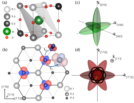
It is thus natural to investigate different surface terminations in the search for 2DEGs with novel and potentially useful properties. Recent theoretical work suggests that (111) oriented perovskites might display particularly intriguing phenomena. Along this direction the ABO3 cubic perovskite structure can be considered as a stacking of ionic AO3 and B-site planes with the B-site ions forming a triangular lattice (see Fig. 1). Two consecutive B-site planes will thus form a honeycomb lattice potentially suitable for realizing novel topological phases Xiao et al. (2011); Yang et al. (2011); Bareille et al. (2014). However, despite the successful creation of 2DEGs at the(111)-oriented interface of STO/LAO Herranz et al. (2012) and at the bare surface of KTaO3 Bareille et al. (2014), little is known to date about their origin and microscopic electronic structure.
Here we use angle resolved photoemission to show that the in-situ cleaved (111) surface of SrTiO3 supports a robust, quantum confined two-dimensional electron system. Our model calculation fully reproduces the observed electronic structure and describes how the 2DEG emerges from the quantum confinement of electrons near the surface due to band bending. Moreover, we demonstrate how the 2DEG can be reversibly depleted and created by alternately exposing the surface to low doses of atomic oxygen and ultraviolet (UV) light, providing insight into the origin of the confining potential.
Single crystals of commercially grown (Crystal GmbH), lightly electron doped SrTi1-xNbxO3(111) () were measured. The Nb doping results in a small residual bulk conductivity and a maximum doping of cm-3, which helps to eliminate charging effects during ARPES but does not otherwise influence our results Spinelli et al. (2010). Samples were cleaved at a pressure lower than mbar at the measurement temperature. ARPES measurements (T K, eV) were performed at the SIS beamline of the Swiss Light Source and the I05 beamline of the Diamond Light Source with an angular resolution of ∘ and an energy resolution of 10 - 20 meV.
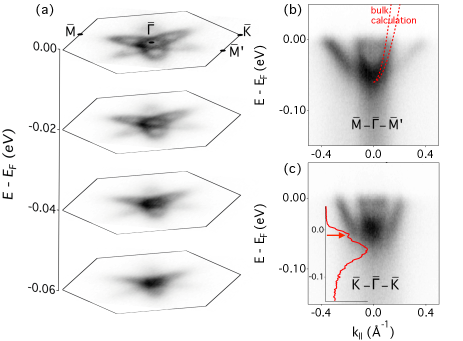
Figure 1 illustrates the different symmetry and atomic arrangement of STO(111) and STO(001) surfaces. While the and orbitals have very different overlap along the [001] confinement direction of STO(001), all orbitals are equivalent modulo a rotation of 120∘ when viewed along the surface normal of STO(111) [see Fig. 1(b)]. This immediately suggests that quantum confinement will not drive a significant orbital polarization in the STO(111) 2DEG, in stark contrast to STO(001) Popović et al. (2008); Salluzzo et al. (2009); Zhong et al. (2013); Khalsa et al. (2013); King et al. (2014), which is indeed what we observe experimentally.
The ARPES Fermi surface [FS] shown in Fig. 2(a) consists of three equivalent elliptical sheets oriented along , consistent with the 3-fold rotational symmetry of the surface 111Since we observe that the matrix elements of photoemission process have a lower symmetry when linearly polarized light is used, the data presented in figure Fig. 2(a) is the sum of spectra taken with right- [C+] and left-handed [C-] circularly polarized light.. The band structure along [Fig. 2(b)] shows a single heavy band, corresponding to the long axis of one of the FS ellipses, which is nearly degenerate at the band bottom with a more dispersive, doubly degenerate band arising from the two remaining FS sheets. Near the Fermi level, additional dispersive spectral weight is observed, indicating a second occupied subband, which is a natural consequence of quantum confinement and is not observed in the bulk. We also confirmed the 2D nature of the charge carriers directly through extensive photon energy dependent measurements (not shown) which reveal no signs of dispersion along within the resolution of the experiment. From the FS area we deduce a 2D carrier density of cm-2. Assuming a constant electron density over approximately 15 Ti layers (33 Å) below the surface, this would correspond to to a 3D density at the surface of cm-3, more than an order of magnitude higher than the nominal bulk doping of our samples. Together, these observations conclusively demonstrate that the observed electronic structure arises from quantum confinement in a surface 2DEG.
Intriguingly, the FS-ellipses we observe are elongated with respect to those of our bulk electronic structure calculations in the (111) plane as indicated by thin red lines in Fig. 2(b). Fitting the measured dispersion over an extended energy range, we find band masses of me and me for the short and long axes of the FS-ellipses respectively, whereas the calculated bulk band masses along the same crystallographic directions are me and me, respectively. This indicates a remarkable reconstruction of the electronic structure, in stark contrast to the case of the STO(001) 2DEG, where the band masses are similar to the bulk except for a moderate low-energy renormalization due to electron-phonon coupling King et al. (2014).
We first discuss these observations on a qualitative level. Since in a 2D system the electronic states have the same energy for all values of the momentum perpendicular to the surface, the Fermi surface of the 2DEG can be approximated by a projection of the 3D bulk band structure (at appropriate doping levels) onto the surface plane. In the case of STO(001), the surface projection is identical to a cut through the bulk FS as is evident from the sketch in Fig. 1(c). Consequently the band masses of the 2DEG closely resemble those of the bulk calculations. In contrast, a projection onto the (111) plane results in elliptical contours that are strongly elongated compared to a cut through the bulk FS as demonstrated in Fig. 1(d), consistent with our observation of enhanced effective masses. Additionally, individual subbands can have different confinement energies depending on their effective masses for motion perpendicular to the surface. Given that where for a square- and for a triangular quantum well respectively, it is immediately clear that orbitals with a large hopping amplitude along the confinement direction will sink deepest in the quantum well. This effect dominates the large lifting of the degeneracy of xy and xz/yz bands observed in the STO(001) 2DEG Popović et al. (2008); Salluzzo et al. (2009); Zhong et al. (2013); Khalsa et al. (2013); King et al. (2014). In the STO(111) 2DEG, on the other hand, all orbitals have the same effective mass along the surface normal of me. Hence, the three orbitals are nearly degenerate at the -point and have a shallow bandwidth comparable to the xz/yz sheets in the (001) 2DEG.
This qualitative understanding is supported by tight-binding supercell calculations based on a non-relativistc ab initio bulk band structure. To calculate the surface electronic structure, a supercell containing 120 Ti atoms stacking along [111] direction was constructed using maximally localized Wannier functions with additional on-site potential terms to account for band bending via an electrostatic potential variation. The tight-binding hamiltonian was solved self-consistently with Poisson’s equation, incorporating an electric field dependent dielectric constant Copie et al. (2009); Bahramy et al. (2012); King et al. (2014). The only adjustable parameter is the total magnitude of the band bending at the surface, which we choose to reproduce the experimentally observed binding energy of the lowest subband ( meV). For simplicity, the calculation assumes a bulk truncated (111) surface devoid of any reconstructions. This is supported by the experimentally observed symmetry of the FS and the absence of backfolded bands, which we confirmed for different photon energies and over multiple Brillouin zones.
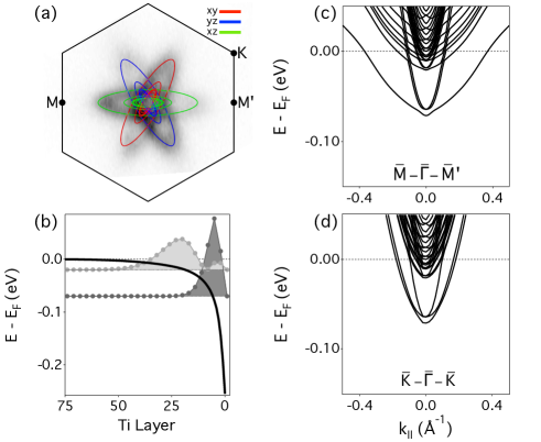
The results of this calculation clearly reproduce the experimentally observed band dispersion and Fermi surface of the lowest subband as shown in Fig. 3. They further indicate a ladder of three higher subbands with progressively more bulk like character. The second subband is predicted just below the Fermi energy, again in good agreement with the experiment. The wave functions of the lowest subband at extend over 15 - 25 Ti layers (34 - 56 Å), and thus nearly an order of magnitude more than the bulk penetration of the first xy subband on STO(001) King et al. (2014). This can be attributed to the lighter effective mass perpendicular to the surface and the correspondingly shallower binding energy. The orbital character of the FS shown in Fig. 3(a) confirms the basic picture that each orbital contributes an equivalent elliptical Fermi surface sheet.
For the remainder of this paper, we discuss the origin of the 2DEG and its relation to interface 2DEGs. Since STO is a band insulator, charge carriers and appropriate electrostatic boundary conditions, namely band bending, are needed to create a 2DEG. In the ideal polar catastrophe scenario for LAO/STO(001), both are provided by the intrinsic electric field in the LAO layer, which allows separation of electrons and holes, resulting in electron accumulation in STO and doped holes on the surface of LAO. While there is strong experimental evidence for this scenario in the case of LAO/STO(001) Nakagawa et al. (2006); Reinle-Schmitt et al. (2012), it clearly cannot apply to a bare STO surface.
Experimentally, we observe that the 2DEG develops on the STO(111) surface only after exposure to intense ultraviolet radiation, just as for the 2DEG of STO(001) Meevasana et al. (2011); King et al. (2014), indicating a common microscopic origin of the quantum confined charge carriers on both surfaces. For the case of STO(001), we proposed earlier that light-induced oxygen desorption might drive the formation of the 2DEG Meevasana et al. (2011). At low temperature, vacancy diffusion will be strongly suppressed and oxygen desorption will be limited to the topmost layer. The system will then try to screen the positively charged vacancies with mobile carriers, which requires band bending such that the edge of the conduction band is dragged below the Fermi level in a narrow layer at the surface.
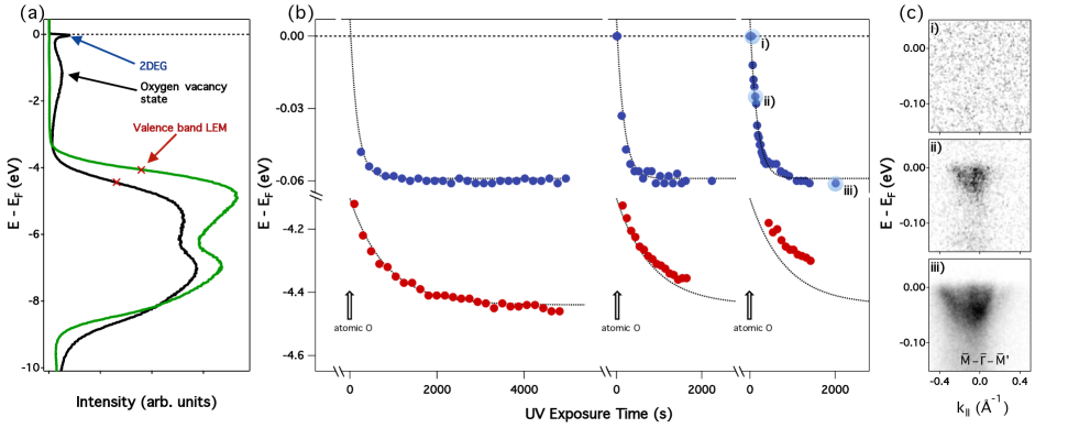
To test this hypothesis we exposed the cleaved surface of STO at low temperature ( K) alternately to UV light and atomic oxygen while monitoring the presence of the 2DEG and changes in the O valence bands. The angle integrated photoemission spectra of the surface after illumination with the synchrotron UV beam ( eV, photons s-1mm-2) for h (black) and immediately after exposure to atomic oxygen (green) are shown in Fig. 4(a) 222The samples were exposed for s to a thermal gas cracker operated at ∘C and a flow of 0.004 sccm ( mbar chamber pressure) resulting in a mixture of atomic and molecular oxygen. The main features of the spectra are the sharp 2DEG peak just below the Fermi level, the O valence band with an onset near eV and an in-gap state around eV, which was attributed to oxygen vacancies in Refs. Meevasana et al. (2010); Aiura et al. (2002); Lechermann et al. (2014); Lin and Demkov (2013). Upon exposure to atomic oxygen the 2DEG peak and the in-gap defect state completely vanish, and concomitant with the depletion of the 2DEG, the VB leading edge mid-point [LEM] shifts towards the Fermi level by meV. Assuming a constant band-gap, this implies a strongly reduced or vanishing band bending following exposure to atomic oxygen. We note that the exact magnitude of the surface band bending is difficult to extract from such data since the photoemission probing depth is comparable to the width of surface band bending. The VB peak will thus contain contributions from unit cells with locally different band energies.
Fig. 4(b) shows the systematic time evolution of the valence band leading edge and the occupied 2DEG bandwidth as the surface is repeatedly exposed to atomic oxygen and UV radiation. The data clearly show that the onset of band bending coincides with near-surface charge accumulation and that both, the bandwidth of the 2DEG, and the depth of the confining potential saturate at long time 333To account for a slight angular misalignment in the first run shown in Fig. 4(b), we corrected the VB leading edge mid-point and 2DEG bandwidth by 23 meV and 40 meV, respectively.. In parallel to this, the in-gap state loses all spectral weight when the surface is treated with atomic oxygen, consistent with the filling of all oxygen vacancies, and recovers as the surface is irradiated again. In Fig. 4(c) we show three dispersion plots obtained after the third consecutive exposure to atomic oxygen. Immediately after oxygen exposure the surface is insulating and no spectral weight is observed at the Fermi level. After s UV exposure a 2DEG with an occupied bandwidth around 30 meV develops. Following longer exposure to UV light, the 2DEG fully recovers the bandwidth and Fermi wave vector of samples that were not treated with atomic oxygen. This indicates that the electronic structure of the 2DEG is largely defined by the electrostatic boundary conditions controlled by the density of charged oxygen vacancies on the surface and is remarkably insensitive to the detailed atomic structure of the surface, which likely changes after exposure to atomic oxygen. We attribute this to the spatial extent of the wave function, which has little weight in the topmost plane and peaks around 6 Ti layers below the surface [see Fig. 3(b)].
Together, our observations conclusively demonstrate that the STO(111) surface supports a 2DEG with 6-fold symmetry, which is quantum confined by a band bending potential induced by surface oxygen vacancies. We further demonstrated control of the 2DEG bandwidth by alternate exposure of the surface to UV light and atomic oxygen providing a broadly applicable route to controlling the carrier density and thus the macroscopic properties of transition metal oxide surface 2DEGs.
Acknowledgements.
We gratefully acknowledge discussions with D. Van der Marel and J.-M. Triscone. This work was supported by Swiss National Science Foundation (200021-146995). PDCK was supported by the UK-EPSRC and MSB by by Grant-in-Aid for Scientific Research (S) (No. 24224009) from the Ministry of Education, Culture, Sports, Science and Technology (MEXT) of Japan.References
- Ohtomo and Hwang (2004) A. Ohtomo and H. Y. Hwang, Nature 427, 423 (2004).
- Caviglia et al. (2008) A. D. Caviglia, S. Gariglio, N. Reyren, D. Jaccard, T. Schneider, M. Gabay, S. Thiel, G. Hammerl, J. Mannhart, and J.-M. Triscone, Nature 456, 624 (2008).
- Reyren et al. (2007) N. Reyren, S. Thiel, A. Caviglia, L. F. Kourkoutis, G. Hammerl, C. Richter, C. W. Schneider, T. Kopp, A.-S. Rüetschi, D. Jaccard, M. Gabay, D. A. Muller, J.-M. Triscone, and J. Mannhart, Science (New York, N.Y.) 317, 1196 (2007).
- Brinkman et al. (2007) A. Brinkman, M. Huijben, M. van Zalk, J. Huijben, U. Zeitler, J. C. Maan, W. G. van der Wiel, G. Rijnders, D. H. a. Blank, and H. Hilgenkamp, Nature Materials 6, 493 (2007).
- Reagor and Butko (2005) D. W. Reagor and V. Y. Butko, Nature Materials 4, 593 (2005).
- Ueno et al. (2008) K. Ueno, S. Nakamura, H. Shimotani, A. Ohtomo, N. Kimura, T. Nojima, H. Aoki, Y. Iwasa, and M. Kawasaki, Nature Materials 7, 1 (2008).
- Chen et al. (2011) Y. Chen, N. Pryds, J. E. Kleibeuker, G. Koster, J. Sun, E. Stamate, B. Shen, G. Rijnders, and S. r. Linderoth, Nano letters 11, 3774 (2011).
- Chen et al. (2013) Y. Z. Chen, N. Bovet, F. Trier, D. V. Christensen, F. M. Qu, N. H. Andersen, T. Kasama, W. Zhang, R. Giraud, J. Dufouleur, T. S. Jespersen, J. R. Sun, A. Smith, J. Nygå rd, L. Lu, B. Büchner, B. G. Shen, S. Linderoth, and N. Pryds, Nature Communications 4, 1371 (2013).
- Meevasana et al. (2011) W. Meevasana, P. D. C. King, R. H. He, S.-K. Mo, M. Hashimoto, A. Tamai, P. Songsiriritthigul, F. Baumberger, and Z.-X. Shen, Nature Materials 10, 114 (2011).
- Santander-Syro et al. (2011) A. F. Santander-Syro, O. Copie, T. Kondo, F. Fortuna, S. Pailhès, R. Weht, X. G. Qiu, F. Bertran, A. Nicolaou, A. Taleb-Ibrahimi, P. Le Fèvre, G. Herranz, M. Bibes, N. Reyren, Y. Apertet, P. Lecoeur, A. Barthélémy, and M. J. Rozenberg, Nature 469, 189 (2011).
- King et al. (2012) P. D. C. King, R. H. He, T. Eknapakul, P. Buaphet, S.-K. Mo, Y. Kaneko, S. Harashima, Y. Hikita, M. S. Bahramy, C. Bell, Z. Hussain, Y. Tokura, Z.-X. Shen, H. Y. Hwang, F. Baumberger, and W. Meevasana, Physical Review Letters 108, 117602 (2012).
- Santander-Syro et al. (2012) A. F. Santander-Syro, C. Bareille, F. Fortuna, O. Copie, M. Gabay, F. Bertran, A. Taleb-Ibrahimi, P. Le Fèvre, G. Herranz, N. Reyren, M. Bibes, A. Barthélémy, P. Lecoeur, J. Guevara, and M. J. Rozenberg, Physical Review B 86, 121107 (2012).
- King et al. (2014) P. D. C. King, S. McKeown Walker, A. Tamai, A. de la Torre, T. Eknapakul, P. Buaphet, S.-K. Mo, W. Meevasana, M. S. Bahramy, and F. Baumberger, Nature Communications 5, 3414 (2014).
- Joshua et al. (2012) A. Joshua, S. Pecker, J. Ruhman, E. Altman, and S. Ilani, Nature Communications 3, 1129 (2012).
- Zhong et al. (2013) Z. Zhong, A. Tóth, and K. Held, Physical Review B 87, 161102 (2013).
- Khalsa et al. (2013) G. Khalsa, B. Lee, and A. H. MacDonald, Physical Review B 88, 041302 (2013).
- Fête et al. (2012) A. Fête, S. Gariglio, A. D. Caviglia, J.-M. Triscone, and M. Gabay, Physical Review B 86, 201105 (2012).
- Kimura et al. (2004) T. Kimura, J. Hamrle, Y. Otani, K. Tsukagoshi, and Y. Aoyagi, Applied Physics Letters 85, 3795 (2004).
- Nakamura et al. (2012) H. Nakamura, T. Koga, and T. Kimura, Physical Review Letters 108, 206601 (2012).
- Xiao et al. (2011) D. Xiao, W. Zhu, Y. Ran, N. Nagaosa, and S. Okamoto, Nature Communications 2, 596 (2011).
- Yang et al. (2011) K.-Y. Yang, W. Zhu, D. Xiao, S. Okamoto, Z. Wang, and Y. Ran, Physical Review B 84, 201104 (2011).
- Bareille et al. (2014) C. Bareille, F. Fortuna, T. C. Rödel, F. Bertran, M. Gabay, O. H. Cubelos, A. Taleb-Ibrahimi, P. Le Fèvre, M. Bibes, A. Barthélémy, T. Maroutian, P. Lecoeur, M. J. Rozenberg, and A. F. Santander-Syro, Scientific Reports 4, 3586 (2014).
- Herranz et al. (2012) G. Herranz, F. Sánchez, N. Dix, M. Scigaj, and J. Fontcuberta, Scientific Reports 2, 758 (2012).
- Spinelli et al. (2010) A. Spinelli, M. A. Torija, C. Liu, C. Jan, and C. Leighton, Physical Review B 81, 155110 (2010).
- Popović et al. (2008) Z. S. Popović, S. Satpathy, and R. M. Martin, Physical Review Letters 101, 256801 (2008).
- Salluzzo et al. (2009) M. Salluzzo, J. C. Cezar, N. B. Brookes, V. Bisogni, G. M. De Luca, C. Richter, S. Thiel, J. Mannhart, M. Huijben, A. Brinkman, G. Rijnders, and G. Ghiringhelli, Physical Review Letters 102, 166804 (2009).
- Note (1) Since we observe that the matrix elements of photoemission process have a lower symmetry when linearly polarized light is used, the data presented in figure Fig. 2(a) is the sum of spectra taken with right- [C+] and left-handed [C-] circularly polarized light.
- Copie et al. (2009) O. Copie, V. Garcia, C. Bödefeld, C. Carrétéro, M. Bibes, G. Herranz, E. Jacquet, J.-L. Maurice, B. Vinter, S. Fusil, K. Bouzehouane, H. Jaffrès, and A. Barthélémy, Physical Review Letters 102, 216804 (2009).
- Bahramy et al. (2012) M. S. Bahramy, P. D. C. King, A. de la Torre, J. Chang, M. Shi, L. Patthey, G. Balakrishnan, P. Hofmann, R. Arita, N. Nagaosa, and F. Baumberger, Nature Communications 3, 1159 (2012), 1206.0564 .
- Nakagawa et al. (2006) N. Nakagawa, H. Y. Hwang, and D. A. Muller, Nature Materials 5, 204 (2006).
- Reinle-Schmitt et al. (2012) M. L. Reinle-Schmitt, C. Cancellieri, D. Li, D. Fontaine, M. Medarde, E. Pomjakushina, C. W. Schneider, S. Gariglio, P. Ghosez, J.-M. Triscone, and P. R. Willmott, Nature communications 3, 932 (2012).
- Note (2) The samples were exposed for s to a thermal gas cracker operated at ∘C and a flow of 0.004 sccm ( mbar chamber pressure) resulting in a mixture of atomic and molecular oxygen.
- Meevasana et al. (2010) W. Meevasana, X. J. Zhou, B. Moritz, C.-C. Chen, R. H. He, S.-I. Fujimori, D. H. Lu, S.-K. Mo, R. G. Moore, F. Baumberger, T. P. Devereaux, D. van der Marel, N. Nagaosa, J. Zaanen, and Z.-X. Shen, New Journal of Physics 12, 023004 (2010).
- Aiura et al. (2002) Y. Aiura, I. Hase, H. Bando, and T. Yasue, Surface Science 515, 61 (2002).
- Lechermann et al. (2014) F. Lechermann, L. Boehnke, D. Grieger, and C. Piefke, arXiv:1401.6105 [cond-mat.mtrl-sci] (2014).
- Lin and Demkov (2013) C. Lin and A. A. Demkov, Physical Review Letters 111, 217601 (2013).
- Note (3) To account for a slight angular misalignment in the first run shown in Fig. 4(b), we corrected the VB leading edge mid-point and 2DEG bandwidth by 23 meV and 40 meV, respectively.