Configurations of Structural Defects
in Graphene and Their Effects on Its Transport Properties
Abstract
The chapter combines analytical (statistical-thermodynamic and kinetic) with numerical (Kubo–Greenwood-formalism-based) approaches used to ascertain an influence of the configurations of point (impurities, vacancies) and line (grain boundaries, atomic steps) defects on the charge transport in graphene. Possible substitutional and interstitial graphene-based superstructures are predicted and described. The arrangements of dopants over sites or interstices related with interatomic-interaction energies governing the configurations of impurities. Depending on whether the interatomic interactions are short- or long-range, the low-temperature stability diagrams in terms of interaction-energy parameters are obtained. The dominance of intersublattice interactions in competition with intrasublattice ones results in a nonmonotony of ordering-process kinetics. Spatial correlations of impurities do not affect the electronic conductivity of graphene for the most important experimentally-relevant cases of point defects, neutral adatoms and screened charged impurities, while atomic ordering can give rise in the conductivity up to tens times for weak and strong short-range potentials. There is no ordering effect manifestation for long-range potentials. The anisotropy of the conductivity along and across the line defects is revealed and gives rise in the conductivity of graphene with correlated line defects as compared with the case of random ones. Simultaneously correlated (and/or ordered) point and line defects in graphene can give rise in the conductivity up to hundreds times vs. their random distribution. On an example of different B or N doping configurations in graphene, results from the Kubo–Greenwood approach are compared with those obtained from DFT method.
PACS: 61.48.Gh, 61.72.Cc, 64.60.Cn, 64.70.Nd, 68.65.-k, 72.80.Vp, 73.63.-b, 81.05.ue
Keywords: Interatomic correlation, atomic ordering, electron scattering, conductivity
Introduction
Pure and structurally perfect graphene has shown outstanding electronic phenomena such as ballistic electron propagation with extremely high carrier mobilities [1] or the quantum Hall effect at room temperature [2]. However, the absence a band-gap in pristine graphene makes its current–voltage characteristic symmetrical with respect to the zero-voltage point and thereby does not allow switching of graphene-based transistors with a high on–off ratio. There are different ways to induce a band-gap in graphene, particularly by the introduction of impurities (point defects) [3].
Generally, different types of defects are always present in crystals due to the imperfection of material production processes. Such lattice imperfections strongly affect different properties in solids. Defect in bulk crystals are investigated for many years, while graphene-based materials are considered only recently. Investigation of its transport properties and understanding factors that affect its conductivity represent one of the central directions of graphene research [4, 5, 6]. This is motivated by both fundamental interest to graphene’s transport properties as well as by potential applications of this novel material for electronics. It is commonly recognized that the major factors determining the electron mobility in graphene are long-range charged impurities trapped on the substrate and strong resonant short-range scatterers due to adatoms covalently bound to graphene [5]. The nature of impurity atoms, acting as the scatterers, is directly reflected in the dependence of the conductivity on the electron density, , and therefore investigation of this function constitutes the focus of experimental and theoretical research [5, 6]. Dopant atoms change the band structure strongly dependent on atomic order and, consequently, provide a tool to govern and even to control electrical conductivity of the graphene-based materials.
Defects, playing role of disorder, can be not always random and stationary, migrating with a certain mobility governed by the activation barrier and temperature [3]. Such migration and relaxation to the equilibrium state as well as the features of the growth technology can result in a correlation or even an ordering in the configuration of point or/and line defects. Experimental observation of correlation in the spatial distribution of disorder have been reported in Ref. [7], where authors addressed enhancement of the conductivity to the effect of correlation between the potassium atoms doping the graphene. This conclusion, in turn, was based on the theoretical predictions in Ref. [8] that the correlations in the position of long-range scatterers strongly enhances the conductivity. It should be noted that the approach in Ref. [8] is based on the standard Boltzmann approach within the Born approximation. However, the applicability of the Born approximation for graphene has been questioned in Ref. [9], where it was shown that predictions based on the standard semi-classical Boltzmann approach within the Born approximation for the case of the long-range Gaussian potential are in quantitative and qualitative disagreement with the exact quantum-mechanical results in the parameter range corresponding to realistic systems. Therefore it is of interest to study the effect of spatial correlation of dopant atoms by exact numerical methods.
Correlation of extended defects, which act as line scatterers, has been also experimentally revealed [10]. Particularly, it concern the line defects in epitaxial and chemically-vapor-deposited (CVD) graphene, where they manifest correlation in their orientation and can be even almost parallel to each other due to the growth technique [10, 11, 12, 13]. Such correlation leads to the anisotropy of diffusivity and conductivity in different directions of graphene sheets [10, 13, 14].
In the present chapter, we consider different (re)distributions of point and one-dimensional (1D) defects in graphene lattice and then ascertain how do their configurations affect the diffusivity and hence conductivity of charge carriers. To do it, we combine analytical (statistical-thermodynamic along with kinetic) approaches and numerical (quantum-mechanical) calculations. An advantage of analytical method is account of interatomic interactions of all (but not only commonly assumed nearest-neighbor) atoms in the system. Numerical (Kubo–Greenwood-formalism-based) calculations are especially suited to treat large graphene sheets containing millions of atoms, i.e. with dimensions approaching realistic systems (here, as well as in Refs. [15, 16], we treat systems having the sizes of and sites corresponding to and nm2). In case of the point defects, we consider random, correlated, and ordered distributions of dopant atoms, calculate the conductivity for each case, and compare obtained results. Line defects are also considered as randomly distributed and orientationally correlated, i.e. with a prevailing direction in their orientation.
Substitutional and Interstitial Graphene-Based Superstructures: Statistical-Thermodynamic Approach
Let us consider possible ordered distributions of impurity atoms over the sites and interstices of honeycomb lattice, namely, graphene-based substitutional and interstitial (super)structures, which are stable against the formation of antiphase boundaries (or splitting up onto antiphase domains).
Substitutional Superlattices
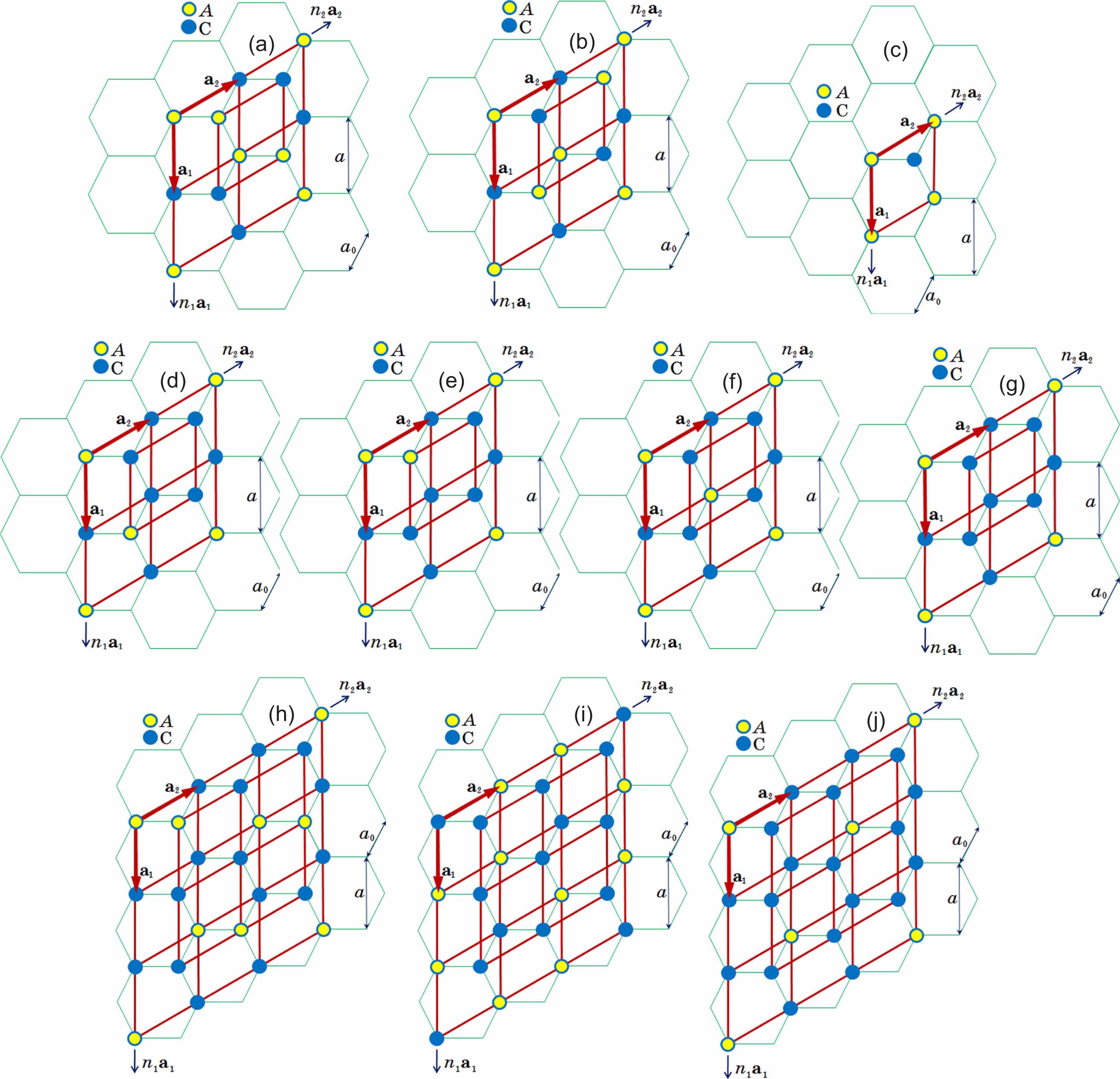
Ordered distributions of substitutional atoms A over the sites of honeycomb lattice at the stoichiometries , (), (), (), (), () are shown in Fig. Substitutional Superlattices. Using the static-concentration-waves’ method and the self-consistent field (mean-field) approximation [17], one can derive expressions for the configurational free energies of different honeycomb-lattice-based structures,
| (1) |
where and denote configurational internal energy and entropy, respectively, and is an absolute temperature.
Specific (per site) configuration-dependent part of the free energies for CA-type substitutional (super)structures in Figs. Substitutional Superlattices(a)–(c) are as follows:
| (2) |
| (3) |
| (4) |
Configurational free energies (per site) for -type substitutional (super)structures presented in Figs. Substitutional Superlattices(h) and (i) are
| (5) |
| (6) |
Configurational free energies (per site) for -type substitutional (super)structures presented in Figs. Substitutional Superlattices(d)–(f) are
| (7) |
| (8) |
| (9) |
Configurational free energy (per site) for -type substitutional (super)structure [Fig. Substitutional Superlattices(j)] reads as
| (10) |
At last, configurational free energy (per site) for -type substitutional (super)structure [Fig. Substitutional Superlattices(g)]:
| (11) |
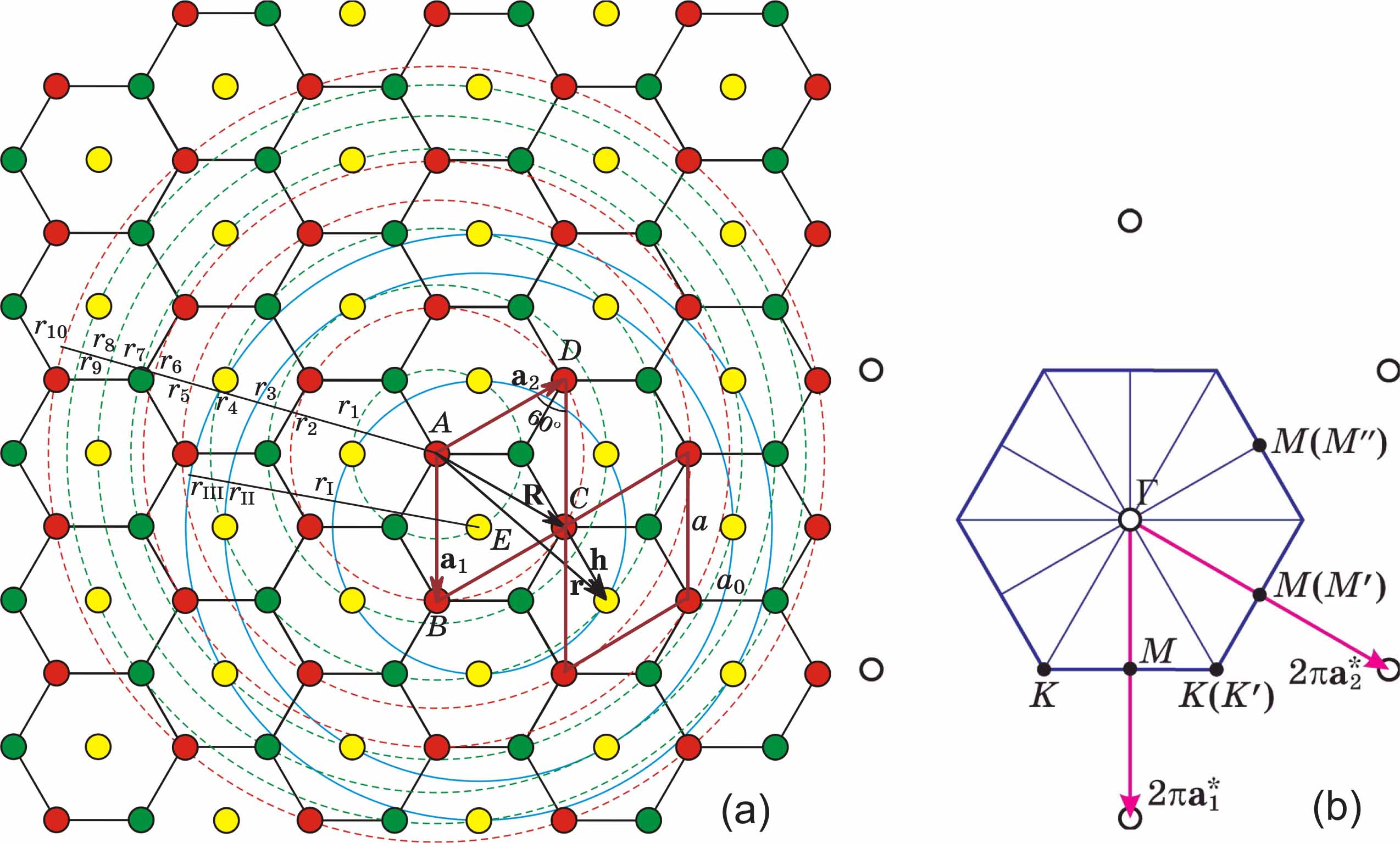
Here, in Eqs. (2)–(11), is an atomic fraction of dopant atoms (), ( or ) are the long-range order (LRO) parameters ( index denotes their total number for a given structure; or ), is a wave vector belonging to the first Brillouin zone of the honeycomb-lattice reciprocal space [see Fig. Substitutional Superlattices(b)] and generating certain superstructure [in detail see Refs. [18, 19, 20, 21]]. Al the thermodynamics of the honeycomb-lattice-based superstructures in Fig. Substitutional Superlattices is defined by interatomic-interaction parameters , , , , , which are connected with pairwise interaction energies , , between , , atoms situated at the sites of -th and -th (, , ) sublattices within the unit sells with origins (“zero” sites) at and . Pairwise interaction energies define so-called mixing energy, which in the literature is known also as “ordering energy” and “interchange energy” [17, 20, 21]. The first-, second-, …, -th-neighbor mixing energies, , , …, [see Fig. Substitutional Superlattices(a)], are commonly used for the analysis of the equilibrium atomic order [19, 21, 22] as well as the ordering kinetics [18, 20, 23]. For the statistical-thermodynamic description of the interatomic interactions in all coordination shells, or arbitrary-range interactions, it is conveniently to apply the Fourier transform, which results to the interatomic-interaction parameters entering into the expressions for the configuration free energies (2)–(11).
Interstitial Superlattices
Denote interstitial atoms in graphene lattice as , and remained vacant positions for these atoms in the interstices as . Each primitive unit cell of the honeycomb lattice contains two sites and one interstice being center of the comb [Fig. Substitutional Superlattices(a)]. An occupation of all interstices by the dopant atoms corresponds to the relative impurity concentration and results to the superstructure-cluster with a maximal atomic fraction of the interstitial dopant atoms, . Its primitive unit cell is shown in Fig. Interstitial Superlattices(a). In this case, applying the static concentration waves’ approach and the self-consistent field (mean-field) approximation [17], one get distribution function for impurity atoms, , and specific configurational free energy (i.e. energy per one interstice) . Here is a Fourier-transform of the mixing energy of and components of interstitial subsystem, , where is energy of effectively pairwise interaction of and () kinds of “atoms” occupying interstices within the primitive unit cells with radii-vectors and , respectively.
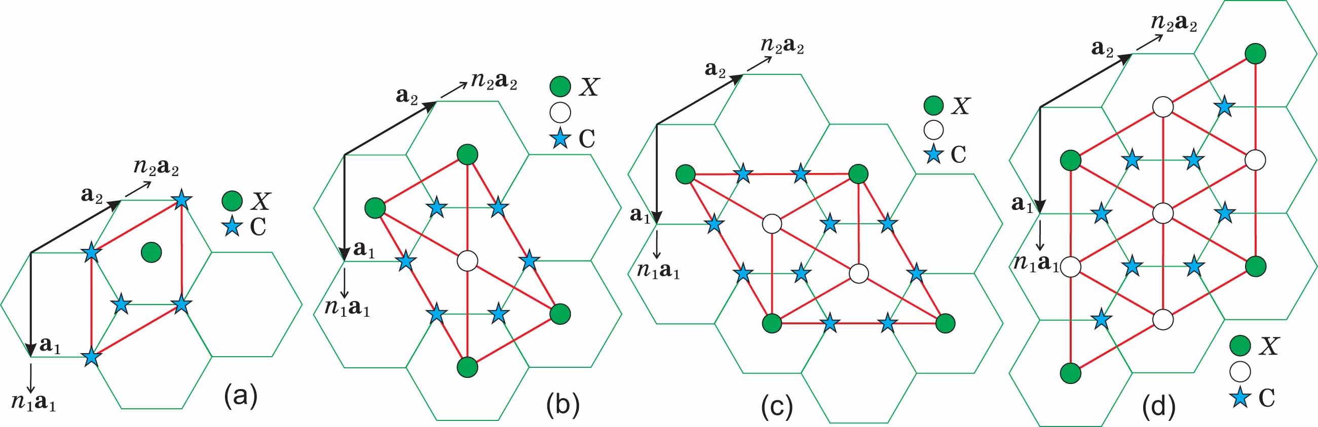
Specific (per interstice) configurational free energy of -type interstitial (super)structure [Fig. Interstitial Superlattices(b)], where in totally ordered state (at 0 K) the relative concentration of interstitial atoms , i.e. their atomic fraction , reads as
| (12) |
Configurational free energy (per interstice) of -type interstitial (super)structure in Fig. Interstitial Superlattices(c) (in the totally ordered state , ) is
| (13) |
In the totally ordered state of -type interstitial (super)structure [Fig. Interstitial Superlattices(d)], and . Its specific configuration-dependent part of the free energy reads as
| (14) |
In conclusion of this section, note that all free-energy equations (2)–(14), being derived within the framework of the self-consistent field approximation, are “governed” by the effective pairwise interactions of – particles only, where for substitutional systems, and for interstitial ones. The main point of such model is that total internal field acting on the substitutional (interstitial) “atom” from the other substitutional (interstitial) and matrix atoms, is replaced with self-averaged (self-consistent) field representing the most probable result of the total interaction of all atoms with distinguished one for a given their distribution generated by the same (self-consistent) field [17, 25, 26].
Low-Temperature Stability of Superstructures
Since each of the stoichiometries among the interstitial superstructures predicts only one ordered distribution of interstitial atoms, as Figs. Interstitial Superlattices(a)–(d) demonstrate, below we pay an attention to the substitutional (super)structural stability only. (Peculiarities of the stability of interstitial graphene-based structures can be found in Ref. [26].)
As follows from Eq. (1), the low-temperature (i.e. at K) stability of a structure, when contribution of the entropy, , to the total free energy, , is small, depends on the internal energy, . At K, the stable is a phase which has the lowest internal energy as compared with other phases of the same composition (here we are neglecting the possibility of the formation of mechanical mixture of pure components and different structures). So, to calculate the low-temperature stability ranges, we minimize the configurational free energy, , setting in Eqs. (2)–(11) . Such minimization is a sufficient stability condition. The necessary condition any superstructure to be appeared is a positive temperature of the stability loss of disordered state with respect to appearance of the long-range atomic order: , i.e., first of all, (, ; ) [17]. These two (necessary and sufficient) conditions can be realized in a certain range of interatomic-interaction parameters entering into Eqs. (2)–(11).
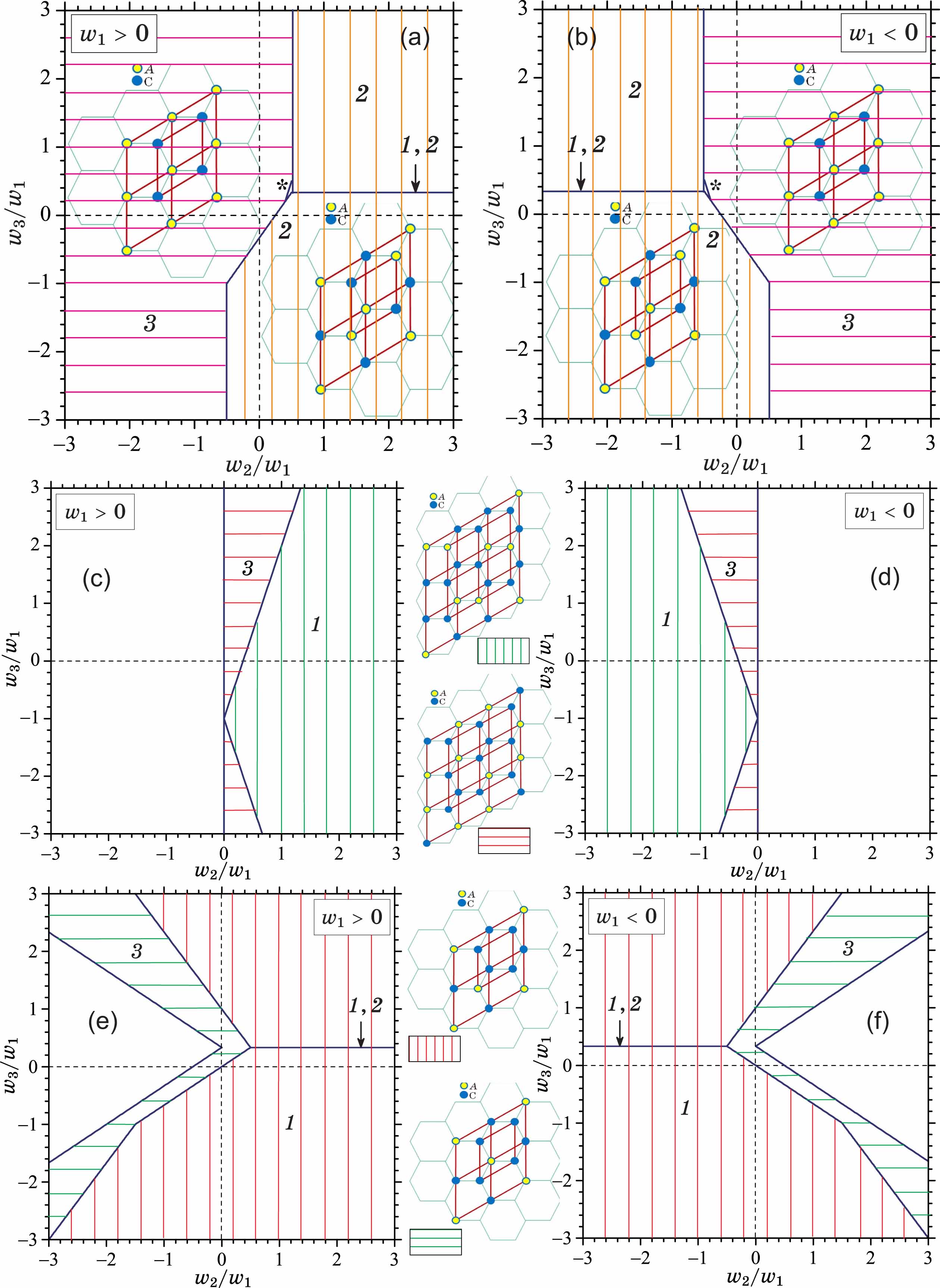
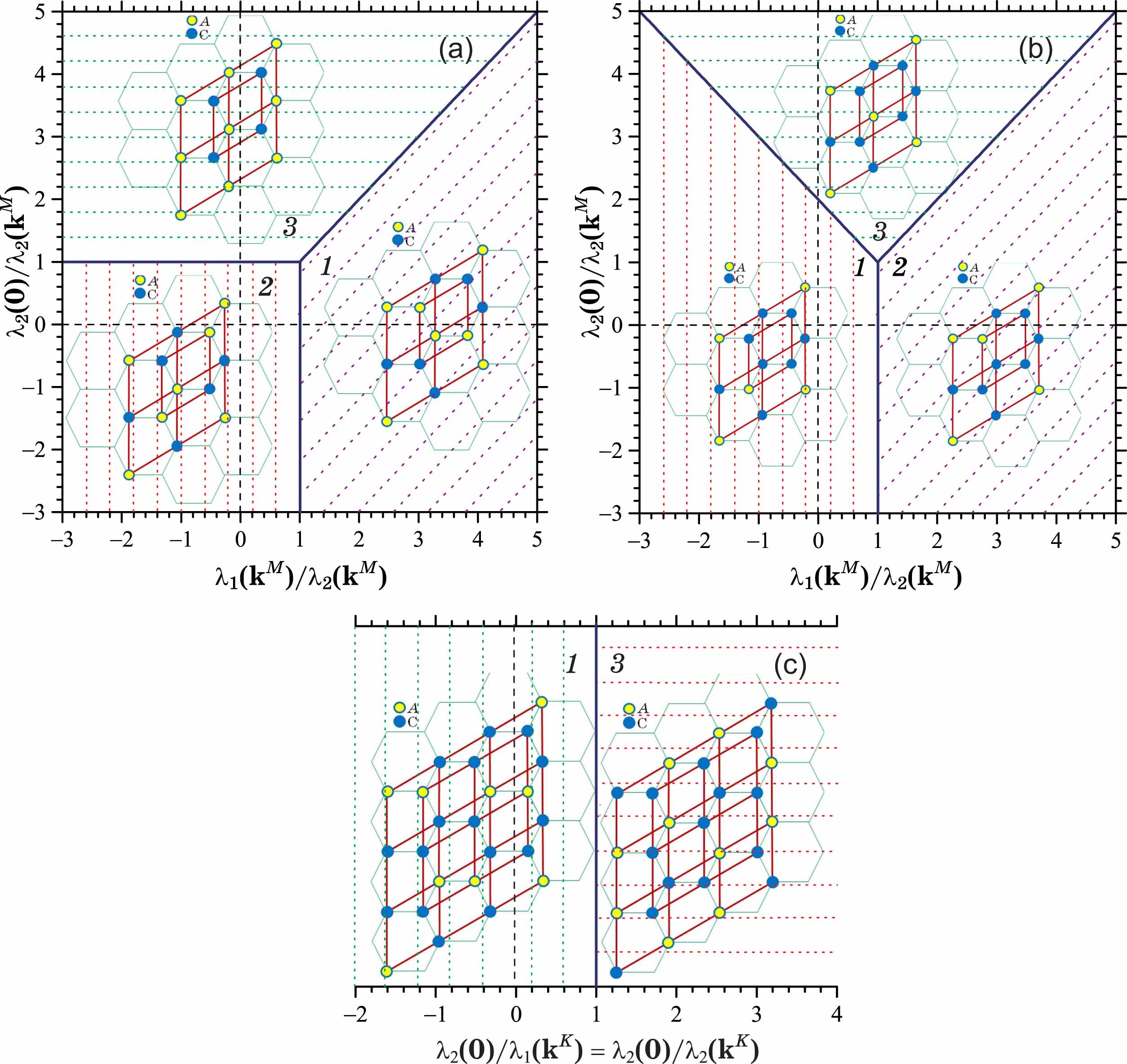
The -, -, and -type superstructures seem the most interesting, since, at these stoichiometries, there are three or two different (nonequivalent) ordered distributions of atoms (see Fig. Substitutional Superlattices). The low-temperature stability regions for these superstructures are represented in Figs. Low-Temperature Stability of Superstructures and Low-Temperature Stability of Superstructures, where the ranges of values of interatomic-interaction parameters providing such a stability are determined. Two cases are considered: firstly (Fig. Low-Temperature Stability of Superstructures), taking into account only first-, second- and third-neighbor mixing energies (, , ), but vanishing mixing energies in other (distant) coordination shells, and, secondly (Fig. Low-Temperature Stability of Superstructures), taking into account mixing energies in all coordination shells.
An account of the third-nearest-neighbor interatomic interactions always provides the stability for the superstructures [Figs. Substitutional Superlattices(c), (d), (f)] in which substitutional dopant atoms are surrounded by the opposite-kind neighbors. However, an account of (only) these (short-range) interactions can be an inadequate to provide the stability for the superstructures [Figs. Substitutional Superlattices(a) and (e)] in which some of the dopant atoms occupy the nearest-neighbor lattice sites. Figure Low-Temperature Stability of Superstructures demonstrates that accounting of the interactions of all atoms contained in the system yields new results as compared with those obtained within the scope of the third-nearest-neighbor interaction approach: every predicted superstructures can be stable at the appropriate values of interatomic-interaction energies.
At the stoichiometries 1/8 and 1/6, there is only one possible ordered arrangement of atoms [see Figs. Substitutional Superlattices(g), (j) and also Eqs. (10), (11)]. Therefore, at low temperatures, - and -type honeycomb-lattice-based superstructures are stable in all set of interatomic-interaction-energy values.
Thus, the third-nearest-neighbor Ising model results in the instability (thermodynamic unfavorableness) of some predicted superstructures. In contrast to this model, the consideration of all coordination shells in the interatomic interactions shows that all predicted honeycomb-lattice-based superstructures are stable at the appropriate values of interatomic-interaction energies. Moreover, some superstructures [ and in Figs. Substitutional Superlattices(a) and (e), respectively] practically may be stable due to the long-range interatomic interactions only.
The problem of stability for graphene-based structures is considered at low temperatures. At finite (or room) temperatures, when LRO parameters in Eqs. (2)–(11) are not equal to unity, , an entropy contribution to the free energy appears. It will result in a shift of the boundaries between the stability ranges in Figs. Low-Temperature Stability of Superstructures and Low-Temperature Stability of Superstructures, but it will not change the qualitative results, particularly, the long-range interatomic-interaction effect on the stability of the graphene-based (super)structures.
Kinetics of the Long-Range Atomic-Order Relaxation
As it is shown above, all interstitial (super)structures (Fig. Substitutional Superlattices) are described by the one LRO parameter only [Eqs. (12)–(14)], while this is not the case for substitutional ones (Fig. Interstitial Superlattices), where two and even there LRO parameters can enter into the free-energy equations (2)–(11). That is why here we consider more complex case—kinetics of the LRO relaxation in the substitutional systems. (Details of the LRO relaxation in the interstitial graphene-based systems can be found in Ref. [26].)
Lets us describe the long-range atomic-order kinetics considering case of exchange (ring) diffusion mechanism governing the atomic ordering in a two-dimensional binary solid solution based on a graphene-type lattice (neglecting the vacancies at the lattice sites). Apply the Önsager-type microdiffusion master equation [17, 20, 23]:
| (15) |
here, is a probability to find -atom in a time at the site, i.e. at the site of -th sublattice within the unit-cell origin position R; () is a relative fraction of -kind (-kind) atom; is a matrix of the Önsager-type kinetic coefficients whose elements represent probabilities of elementary exchange-diffusion jumps of a pair of and atoms at and sites of the -th and -th sublattices composing the honeycomb lattice and displaced with respect to each other by the vector h (; ; , ).
If the vacancy content is small, we have almost identity for the single-site occupation-probability functions of and C atoms distribution over the honeycomb-lattice site: . Then it is enough to consider an exchange-microdiffusion migration of only dopant atoms in terms of the time dependence of only probabilities . One can use kinetics equation (15) to describe microdiffusion by the other mechanisms since semi-phenomenological Eq. (15) does not contain a certain microdiffusion mechanism. Considering of any other mechanism does not require changing of the type of Eq. (15), since diffusion mechanism is defined by the kinetic coefficients , which should be linked with microscopic characteristics of the system (energy barrier heights for atomic jumps, thermal vibrational frequencies of atoms at the sites, vacancy concentration) and external thermodynamic parameters (temperature etc.)
Condition of the conservation of each kind of atoms in the system, assumption that any site is obligatory occupied by C or atom, Önsager-type symmetry relations, representation of thermodynamic driven force (as well as ) as a superposition of the concentration waves, followed by the Fourier transform of both members in Eq. (15), yield us differential equations of the time evolution of the LRO parameters, :
| (16) |
where is the Fourier-component of a concentration-dependent combination of kinetic coefficients , , and particular expressions for are presented in Refs. [20, 23]. It is convenient to solve Eq. (16) in terms of the reduced time and temperature .
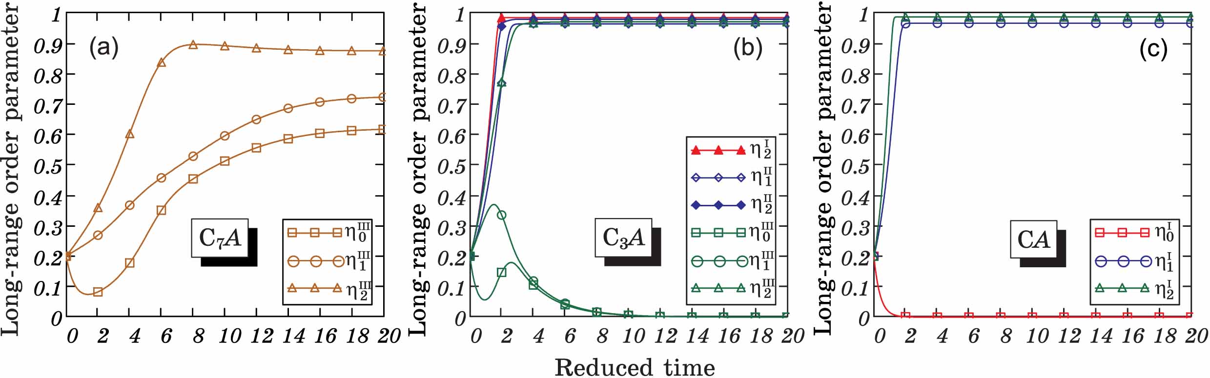
Curves in Fig. Kinetics of the Long-Range Atomic-Order Relaxation are numerical calculations of the kinetic equations (16) for the ordered , , and superstructural types at the reduced temperature and certain interatomic-interaction parameters , given as an example. These values correspond to the certain point [] on the stability diagrams for and superstructures in Figs. Low-Temperature Stability of Superstructures(a) and (b). This point indicates what superstructure is energetically favorable (stable) between the three possible ones at the given stoichiometry. Stability diagrams in Fig. Low-Temperature Stability of Superstructures are obtained for the absolute zero temperature, while the kinetic curves in Fig. Kinetics of the Long-Range Atomic-Order Relaxation are calculated for the nonzero temperature. Nevertheless, one can easy see a correspondence between the statistical-thermodynamic and kinetics results. Results of the latter improve previous ones; particularly, for the mentioned point on the diagrams, energetically favorable is a structure described by the LRO parameter, which relaxes to its equilibrium state being the highest between the other equilibrium, stationary, and current values of the LRO parameters of the given composition (see Figs. Low-Temperature Stability of Superstructures(a), (b) and Figs. Kinetics of the Long-Range Atomic-Order Relaxation(b), (c).
Figures Kinetics of the Long-Range Atomic-Order Relaxation(a) and (b) clear demonstrate that kinetic curves for the LRO parameters of the - and -type (super)structures, described by two or three order parameters, can be nonmonotonic. The nonmonotony is caused not only by the presence of two interpenetrating sublattices composing the honeycomb lattice, but also by the dominance of the intersublattice mixing (interatomic-interaction) energies in their competition with intrasublattice interaction energies.
Influence of Correlated and/or Ordered Impurities on Conductivity of Graphene: Numerical Calculations
This section is devoted to the investigation of influence of the spatial correlation and ordering of impurities, acting as a “disorder” in graphene, on its conductance using a numerical quantum mechanical approach. We utilize the time-dependent real-space quantum Kubo–Greenwood method [15, 16, 27, 28, 29, 30, 31, 32, 33], which allows us to study experimentally-relevant large graphene sheets containing millions of atoms. We consider models of disorder appropriate for realistic impurities that might exhibit correlations, including the Gaussian potential describing screened charged impurities and the short-range potential describing neutral adatoms.
We model electron dynamics in graphene using the standard -orbital nearest neighbor tight-binding Hamiltonian defined on a honeycomb lattice [5, 6],
| (17) |
where and are the standard creation and annihilation operators acting on a quasi-particle on the site . The summation over runs over the entire graphene lattice, while is restricted to the sites next to ; eV is the hopping integral for the neighboring C atoms and with distance nm between them (Fig. Substitutional Superlattices), and is the on-site potential describing impurity scattering.
In the present study we consider both short- and long-range impurities. The short-range impurities represent neutral adatoms on graphene and are modeled by the delta-function scattering potential for electrons
| (18) |
where is the number of impurities on a graphene sheet. Estimations based on ab initio calculations and the T-matrix approach for common adatoms provide typical values for the on-site potential [34, 35, 36, 37], e.g., for hydrogen, .
The long-range potential is appropriate for screened charged impurities situated on graphene and/or dielectric substrate. We model them by the Gaussian scattering potential commonly used in the literature [5, 6, 9]
| (19) |
where () is the radius-vector of the () site, is the effective potential radius, and the potential height is uniformly distributed in the range with being the maximum potential height.
We consider three cases of impurity distribution, random (uncorrelated), correlated, and ordered. In the first case, the summation in Eqs. (18), (19) is performed over the random distribution of impurities over the lattice sites. In the second case impurities are no longer considered to be randomly distributed and to describe their spatial correlation we adopt a model used in Ref. [8] introducing the pair distribution function ,
| (20) |
where is the distance between two impurities and the correlation length defines the minimum distance that can separate two impurities. Note, that for the randomly distributed (totally uncorrelated) impurities . The largest distance depends on the relative impurity concentration : the smaller the concentration the larger . At last, in the third case, the ordered distribution of impurity atoms over the sites of both sublattices is described by the single-site occupation-probability functions, which can be derived by the method of the static concentration waves [17]. Particularly, for -type () substitutional superstructure in Fig. Substitutional Superlattices(g), they are [18, 19, 20]
| (21) |
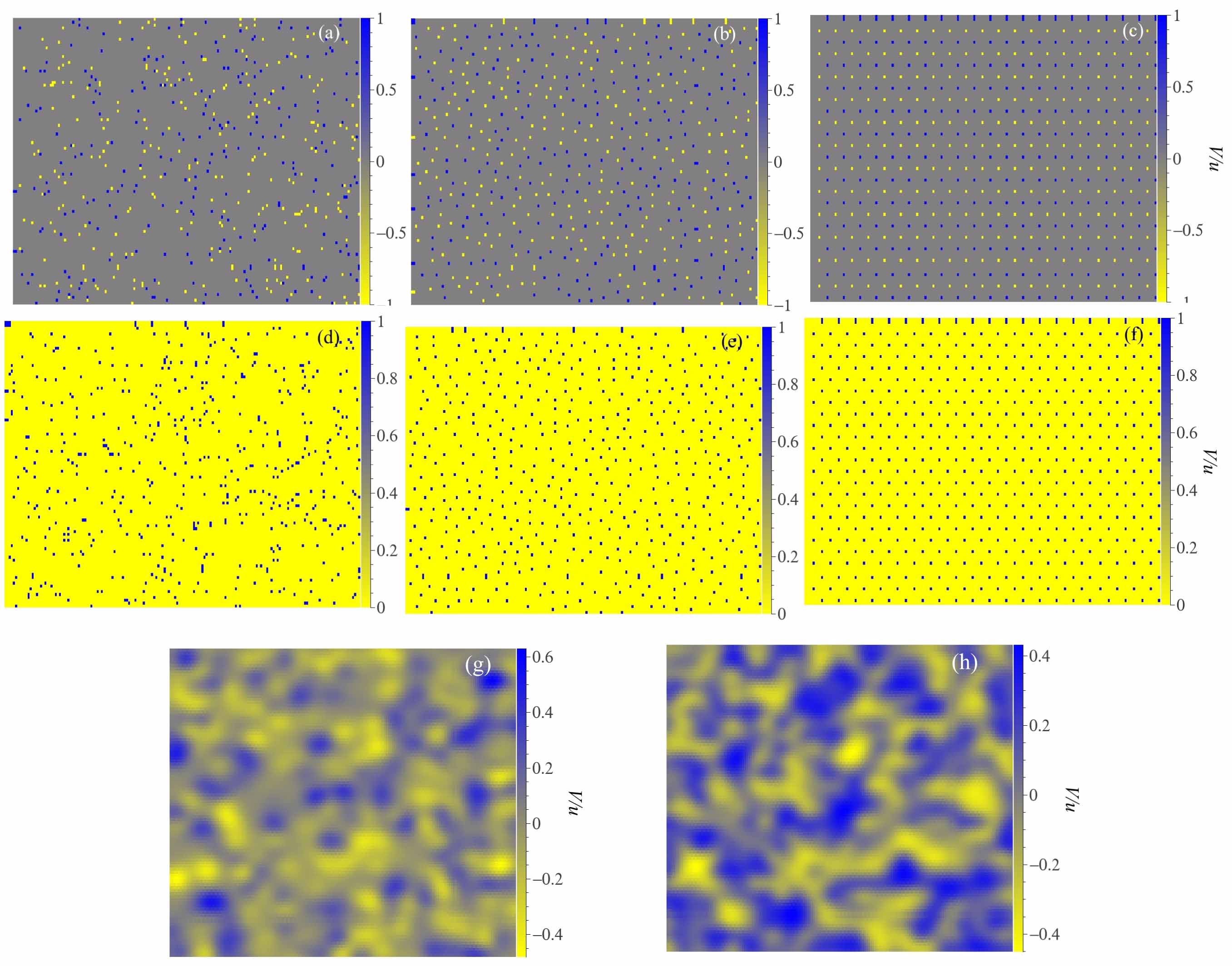
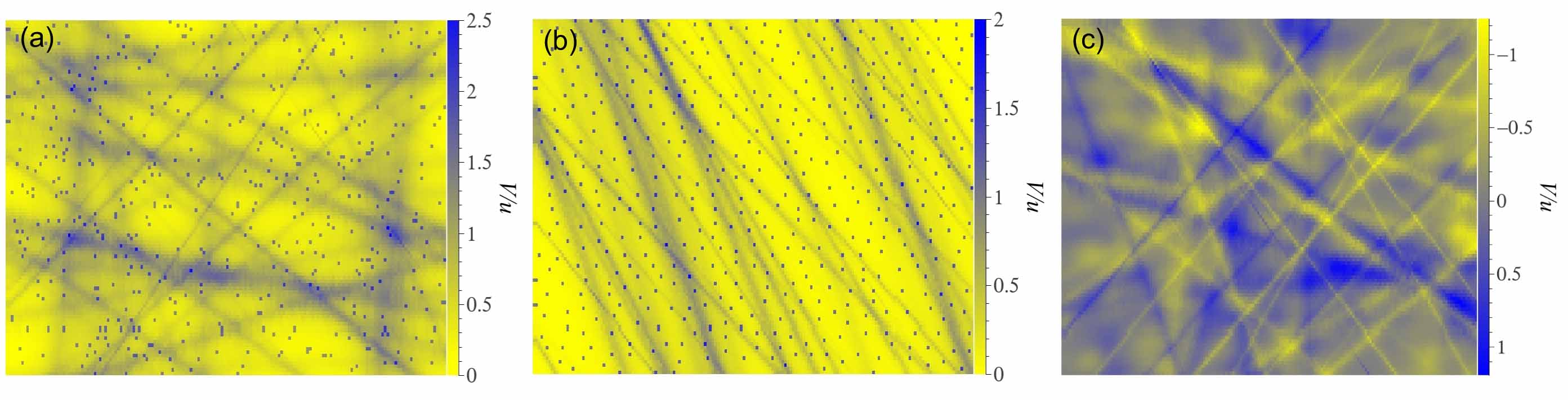
are integers. and possess four values [, , , ] over all lattice sites. The representative examples of random and correlated distributions for the cases of the short- and long-range potentials are shown in Fig. Influence of Correlated and/or Ordered Impurities on Conductivity of Graphene: Numerical Calculations.
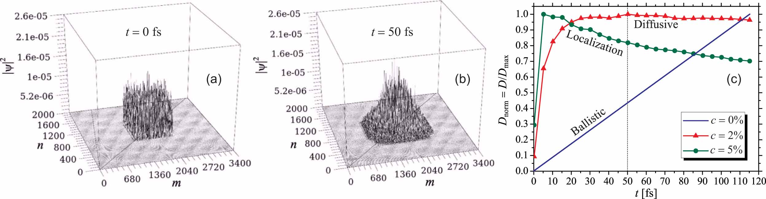
The transport properties of graphene sheets can be calculated on the basis of the time-dependent real-space Kubo formalism, extracting the dc conductivity from the wave packet temporal dynamics governed by the time-dependent Schrödinger equation [15, 16, 27, 28, 29, 30, 31, 32, 33].
A central quantity in the Kubo–Greenwood approach is the mean quadratic spreading of the wave packet along the -direction at the energy , , where is the position operator in the Heisenberg representation, and is the time-evolution operator [wave-packet propagation is visualized in Figs. Influence of Correlated and/or Ordered Impurities on Conductivity of Graphene: Numerical Calculations(a), (b)]. Starting from the Kubo–Greenwood formula for the dc conductivity [38]
| (22) |
where is the -component of the velocity operator, is the Fermi energy, is the area of the graphene sheet, and factor 2 accounts for the spin degeneracy, the conductivity can then be expressed as the Einstein relation,
| (23) |
where is the density of electronic sates (DOS) per unit area (per spin), and the time-dependent transport coefficient (commonly called as diffusivity) relates to as
| (24) |
Further, we are interested in the diffusive transport regime at [Fig. Influence of Correlated and/or Ordered Impurities on Conductivity of Graphene: Numerical Calculations(c)], when, neglecting the quantum-localization effects, the coefficient reaches its maximum. Therefore, following Refs. [31, 32], we replace in Eq. (23) such that the diffusion-controlled dc conductivity is defined as
| (25) |
Note that in most experiments, the conductivity is measured as a function of electron density . We calculate the electron density as where cm-2 is the density of the positive ions in the graphene lattice compensating the negative charge of the -electrons [for the ideal graphene lattice, i.e. without defects, at the neutrality point ]. Combining the calculated with given by Eq. (25), one can obtain the required dependence of the conductivity . Details of numerical calculations of DOS, , and are given in Ref. [15].
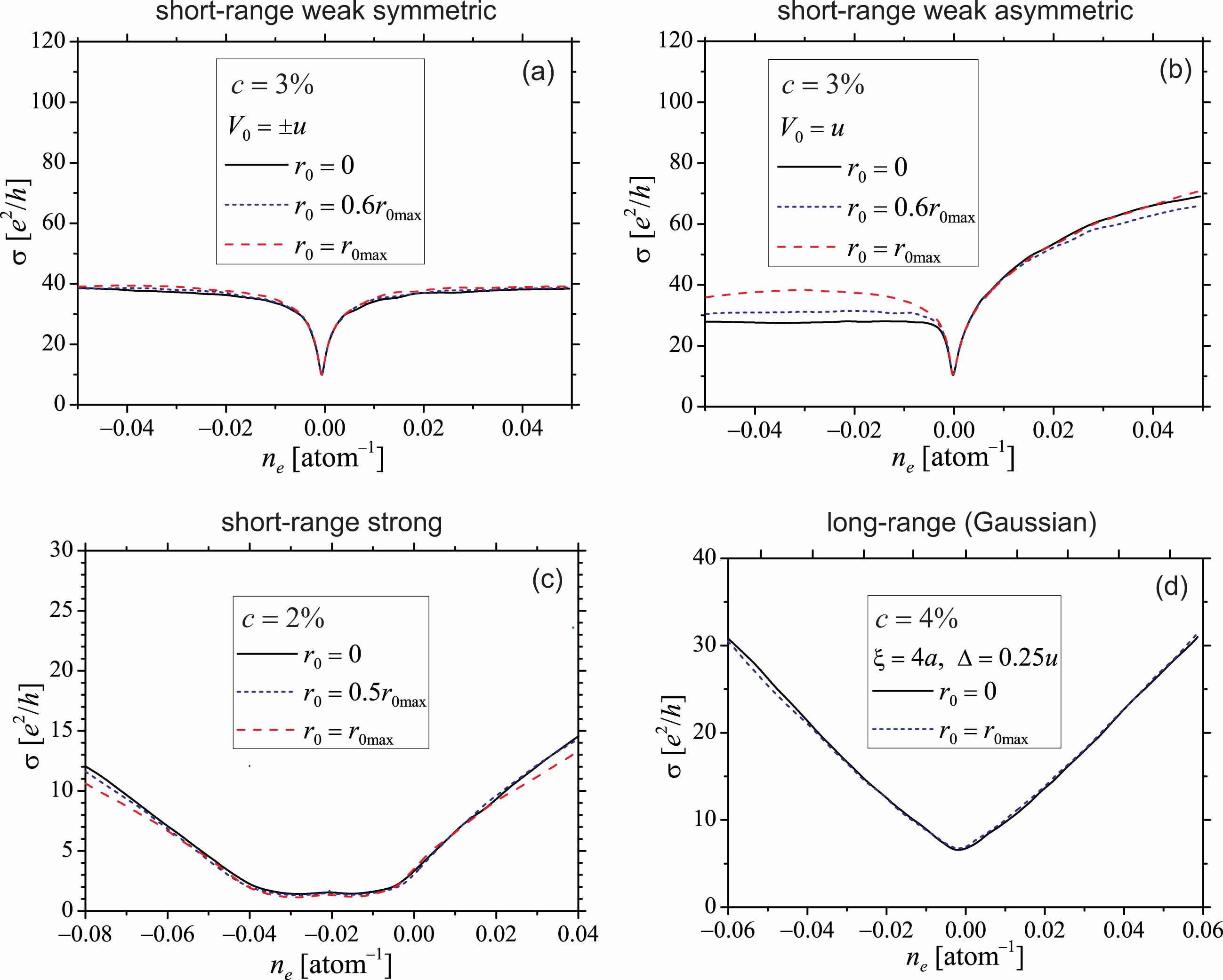
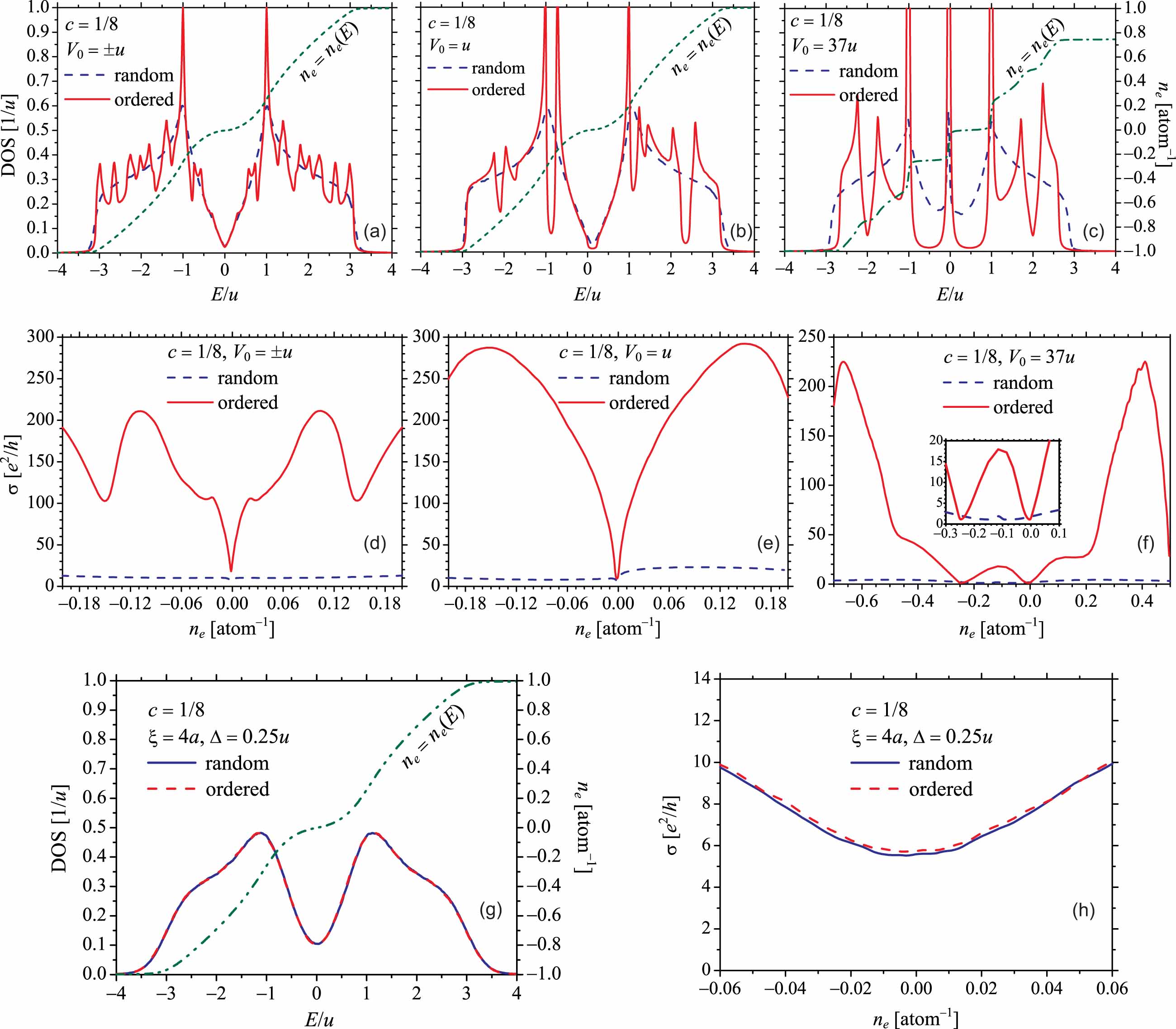
Figure Influence of Correlated and/or Ordered Impurities on Conductivity of Graphene: Numerical Calculations shows the electron-density dependencies of the conductivity for random and correlated impurities modeled by different scattering potentials, where positive and negative values of correspond to different kinds of charge carriers: electrons and holes. As Figure Influence of Correlated and/or Ordered Impurities on Conductivity of Graphene: Numerical Calculations demonstrates,t for the most important, experimentally relevant cases of point defects, namely the strong short-range potential and the long-range Gaussian potential, the correlation in the distribution of impurity atoms does not affect the conductivity of the graphene as compared to the case when they are distributed randomly. This represent the main result for the case of the correlation. We find that the correlations lead to the enhancement of the conductivity only for the case of the weak short-range potential and only when the potential is asymmetric, i.e. or No enhancement of the conductivity is found for the symmetric weak short-range potential,
As it was mentioned in the introduction, in the recent experiment [7] the temperature increase of the conductivity was attributed to the enhancement in the spatial correlation of the adsorbed potassium ions. Numerical findings do not sustain this interpretation, the obtained here results strongly suggest that the enhancement of the conductivity reported in Ref. [7] is most likely caused by other factors not related to the correlations of impurities. The numerical calculations do not support also theoretical predictions in Ref. [8] that the correlations in the impurity positions for the long-range potential lead to the enhancement of the conductivity. This can be attributed to the utilization of the standard Boltzmann approach within the Born approximation which is not valid for the case of a long-range potential in the parameter range corresponding to realistic systems.
In contrast to the case of the correlated impurities, the ordered short-range weak and essentially strong impurities can strongly affect charge transport in graphene [Fig. Influence of Correlated and/or Ordered Impurities on Conductivity of Graphene: Numerical Calculations(a)–(f)]. In the DOS-curves discrete energy levels appear [Figs. Influence of Correlated and/or Ordered Impurities on Conductivity of Graphene: Numerical Calculations(a)–(c)] and broaden as impurity concentration or/and scattering potential increases. This oscillations (peaks) in the DOS and therefore in the conductivity are caused by the strongly periodic potential, describing periodic positions of impurity atoms “precipitating” a certain superstructure (in the given case, with the stoichiometry ). It is clear seen from Fig. Influence of Correlated and/or Ordered Impurities on Conductivity of Graphene: Numerical Calculations that the conductivity curves for the ordering case rise up to tens times for the short-range weak [Figs. Influence of Correlated and/or Ordered Impurities on Conductivity of Graphene: Numerical Calculations(d), (e)] and especially strong [Fig. Influence of Correlated and/or Ordered Impurities on Conductivity of Graphene: Numerical Calculations(f)] scatterers as compared with the case of the randomly-distributed scattering centers. However, as for the correlation, ordering does not affect nor density of electronic states nor conductivity for the long-range (Gaussian) scattering potential (Figs. Influence of Correlated and/or Ordered Impurities on Conductivity of Graphene: Numerical Calculations(g), (h).
Anisotropy and Increase in Conductivity due to the Orientational Correlation of Line Defects in Graphene
Nowadays, several techniques are capable of producing high-quality, large-scale graphene. These include CVD-grown graphene on transition metal surfaces [39] and epitaxial graphene growth on SiC [40]. Usually, the growth of graphene by the CVD-method requires to use metal surfaces with hexagonal symmetry, such as the (111) surface of cubic or the (0001) surface of hexagonal crystals [3]. The mismatch between the metal-substrate and graphene causes the strains in the latter, reconstructs the chemical bonds between the carbon atoms and results in formation of two-dimensional (2D) domains of different crystal orientations separated by one-dimensional defects [3, 41, 42, 43]. The nucleation of the graphene phase takes place simultaneously at different places, which leads to the formation of independent 2D domains matching corresponding grains in the substrate. A line defect appears when two graphene grains with different orientations coalesce; the stronger the interaction between graphene and the substrate, the more energetically preferable the formation of line defects is. These line defects accommodate localized states trapping the electrons, originating lines of immobile charges that scatter the Dirac fermions in graphene. It is well established that the presence of grains and grain boundaries in three-dimensional polycrystalline materials can strongly affect their electronic and transport properties. Hence, in principle, the role of such structures in 2D materials, such as graphene, can be even more important because even a single line defect can divide and disrupt the crystal [3]. Theoretical results [16, 44] improve that the presence of charged line defects strongly affect the transport properties of CVD-graphene. Such effect becomes more weighty due to existence of ordered line defects in CVD-synthesized graphene [13].
In epitaxial graphene the surface steps caused by substrate morphology are spatially correlated and act as line scatterers for the charge carriers [10]. Epitaxial graphene films grown on SiC [10, 12] (by SiC decomposition) or on Ru [11] (by CVD method) comprise two distinct self-organized periodic regions of terrace and step, leading to ordered graphene domains [11]. Experimental measurements show an increase of the resistance with the step density [45], the step heights [46], the step bunching [47]. Also, an anisotropy of the conductivity in the parallel and perpendicular directions to the steps is revealed, which is due to to higher defect abundance in the step regions [10, 14]. Substrate steps alone increase the resistivity in several times relative to a perfect terrace [46] with the ratio of the estimated electron mobilities in the terrace and step regions being about 10:1 [10]. Despite the strong curvature of graphene in the vicinity of steps, a structural deformation contributes only little to electron scattering [48]. For the SiC substrate, the dominant scattering mechanism is provided by the sharp potential variations in the vicinity of the step due to the electrostatic doping from the substrate strongly coupled with graphene in the step regions [48].
Several theoretical studies have been recently reported addressing transport properties of graphene with a single graphene boundary [49, 50, 51] or polycrystalline graphene with many domain boundaries [27]. On the other hand, much less attention has been paid to the effect of charge accumulation at these boundaries due to self-doping. Transport properties of graphene with 1D charged defects has been studied in Ref. [44] using the Boltzmann approach within the first Born approximation. It has been demonstrated that such approximation is not always applicable for the description of electron transport in graphene even at finite (non-zero) electronic densities [37, 52, 9]. Following Ref. [16], below we present results of investigations of the impact of extended charged defects in the transport properties of graphene by an exact numerical approach based on the time-dependent real-space quantum Kubo method [15, 16, 27, 28, 29, 30, 31, 32, 33], which is especially suited for experimentally-relevant systems containing millions of atoms.
Since line defects can be thought as lines of reconstructed point defects [41, 3, 42, 43], we model a 1D defect as point defects oriented along a fixed direction (corresponding to the line direction) in the honeycomb lattice. The electronic effective potential for a charged line within the Thomas–Fermi approximation was first obtained in Ref. [44]. If there are such charged lines in a graphene lattice, the effective scattering potential reads as
| (26) |
where is a potential height, is a distance between the site and the -th line, is the Thomas–Fermi wave-vector defined by the electron Fermi velocity and the Fermi momentum (related to the electronic carrier density controlled applying the back-gate voltage). Here, denotes the electron charge. The Thomas–Fermi wave-vector is also commonly expressed as a function of graphene’s structure constant according to . We consider two cases: symmetric (attractive and repulsive), , and asymmetric (repulsive), , potentials, where are chosen randomly in the ranges and , respectively, with being the maximal potential height. In order to simplify numerical calculations, we fit the potential (26) by the Lorentzian (Cauchy) function
| (27) |
where the fitting parameters , , can be calculated from the least-squares method [16]. The typical shapes of the effective potential for both symmetric (attractive–repulsive) and asymmetric (repulsive) cases are illustrated in Fig. Anisotropy and Increase in Conductivity due to the Orientational Correlation of Line Defects in Graphene.
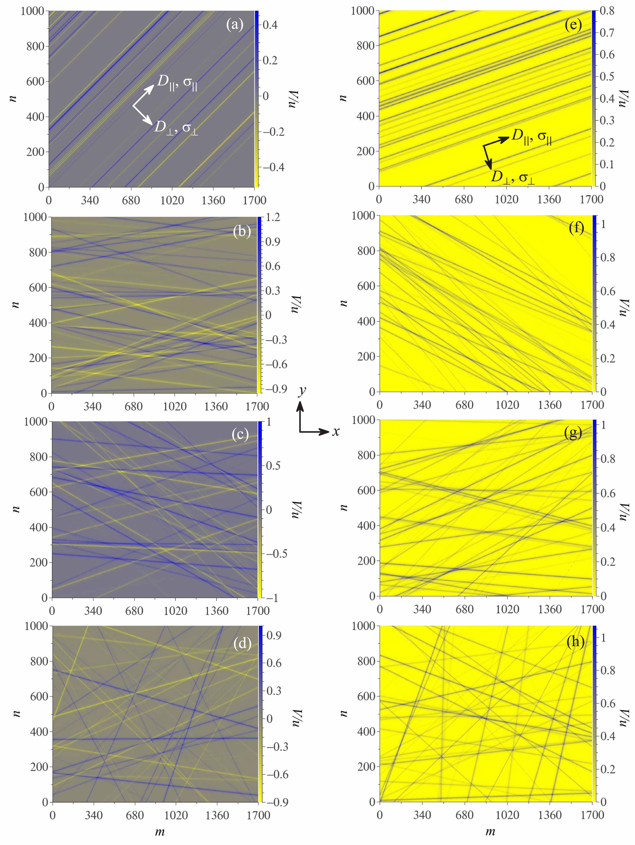
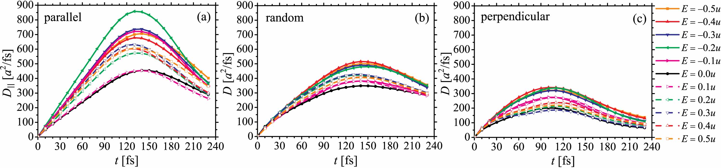
Figure Anisotropy and Increase in Conductivity due to the Orientational Correlation of Line Defects in Graphene shows the time evolution of the diffusion coefficient within the energy interval for the symmetric (attractive–repulsive) potential for three different cases of orientation distribution of 50 line defects. (Transport curves for the case of the asymmetric potential exhibit a similar behavior and are not shown here). In the first and the third cases, Figs. Anisotropy and Increase in Conductivity due to the Orientational Correlation of Line Defects in Graphene (a) and (c), the transport coefficients and are calculated respectively along and across 50 parallel-oriented lines (distance between them is different and random). In the second case, Fig. Anisotropy and Increase in Conductivity due to the Orientational Correlation of Line Defects in Graphene(b), the lines are randomly distributed, which results in the isotropic transport, i.e. . As expected, the electron transport along the lines are higher than those across the lines, whereas .
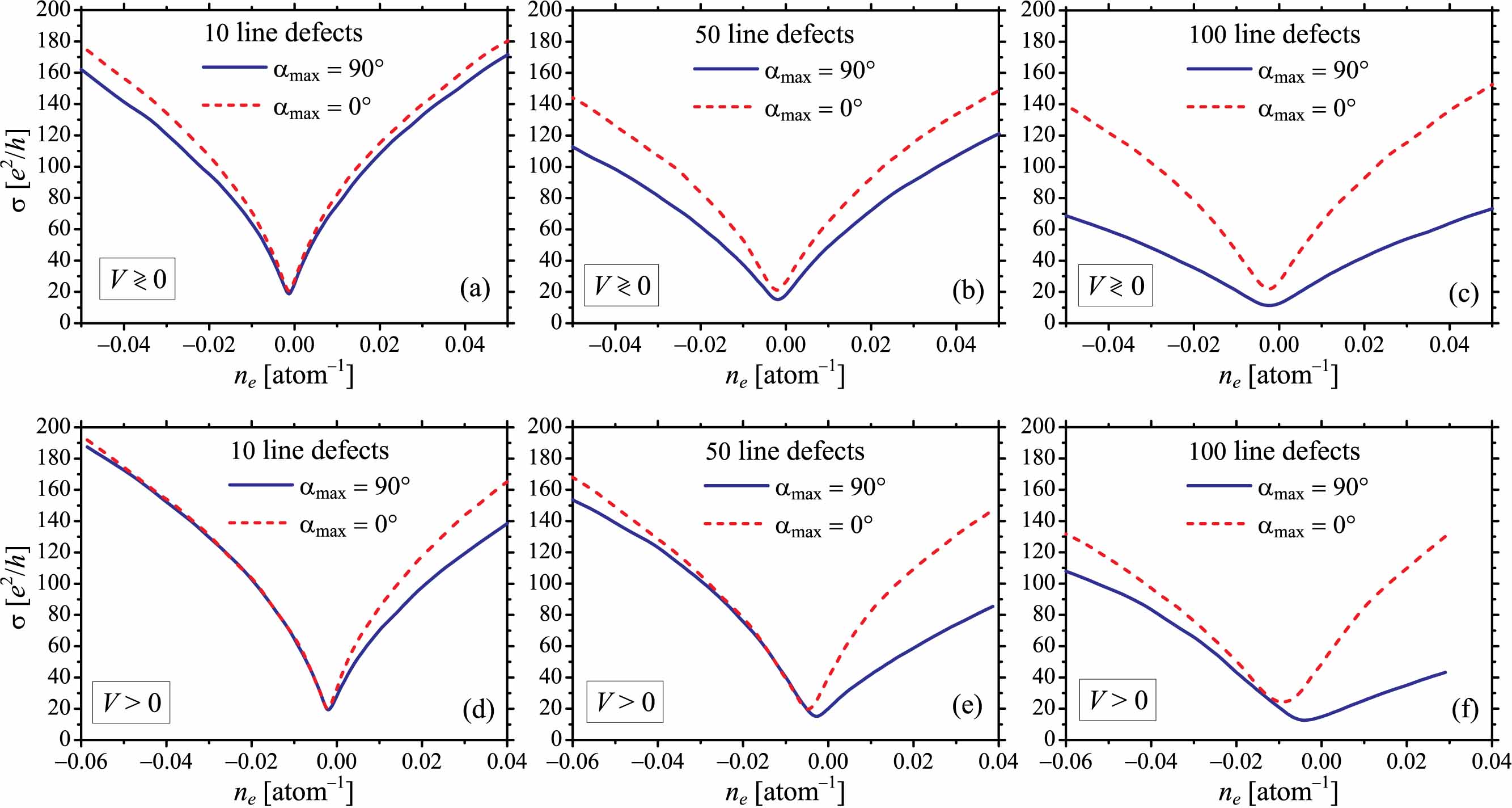
In Figure Anisotropy and Increase in Conductivity due to the Orientational Correlation of Line Defects in Graphene, we show the electron-density dependence of the conductivity of graphene sheets with different (10, 50, 100) number of linear defects for the cases of symmetric and asymmetric potentials. First, for a given defect concentration the conductivity of graphene with the correlated line defects, , increases in comparison to the case of uncorrelated defects, (see Fig. Anisotropy and Increase in Conductivity due to the Orientational Correlation of Line Defects in Graphene). This can be contrasted with the case of point defects,when the correlation in the defect position practically does not affect the conductivity (Fig. Influence of Correlated and/or Ordered Impurities on Conductivity of Graphene: Numerical Calculations). Second, for a given electron density, the relative increase of the conductivity for the case of fully correlated line defects in comparison to the case of uncorrelated ones is higher for a larger defect density. This is an expected result since correlation effect manifests itself stronger for a larger number of objects-to-be-correlated—line defects at hand.
Finally, note some features that show the obtained dependencies in (CVD and epitaxial) graphene, where the charged line-acting defects are believed to represent the limiting scattering mechanism.
First, the conductivity exhibits a pronounced sublinear electron-density dependence and depends weakly on the Thomas–Fermi screening wavelength [16]. Our numerical calculations are consistent with the recent experimental results [39, 53, 54] that also exhibit sublinear density dependence of . This provides an evidence in support that the line defects represent the dominant scattering mechanism in both CVD and epitaxial graphene [39, 44, 53].
Second, the conductivities of samples with different line configurations exhibit significant variations between each other [16]. This is in strong contrast to the case of short- and long-range point scatterers where corresponding conductivities of samples of the same size and impurity concentrations practically did not show any noticeable differences for different impurity configurations [15]. We attribute this to the fact that in contrast to point defects, the line defects are characterized not only by their positions, but also by directions (orientations) and their intersections as well. Such additional characteristics result in much more possible distributions of the potential which, in turn, leads to the differences in the conductivity curves.
Third, for the symmetric potential the conductivity curves are symmetric with respect to the neutrality (Dirac) point, while the asymmetric one leads to the asymmetry in the conductivity, cf. Figs.Anisotropy and Increase in Conductivity due to the Orientational Correlation of Line Defects in Graphene(a)–(c) and (d)–(f). Such the asymmetry between the holes and electrons, being also seen in transport calculations in graphene with point [15, 31, 55, 56] and line [16, 44] defects, causes a quantitatively different conductivity enhancements for the orientationally-correlated line defects as Fig. Anisotropy and Increase in Conductivity due to the Orientational Correlation of Line Defects in Graphene demonstrates.
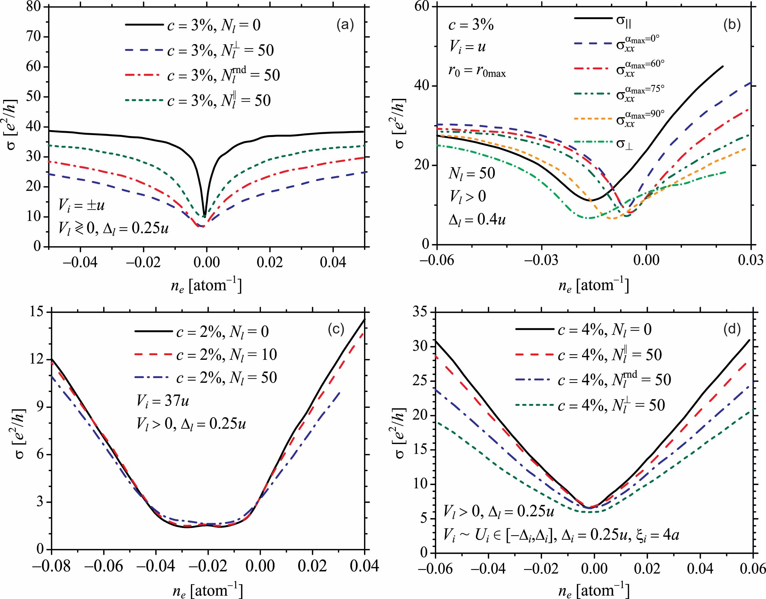
In conclusion of the section note that the presence of both defect types, point and line ones (Fig. Anisotropy and Increase in Conductivity due to the Orientational Correlation of Line Defects in Graphene), which seems even more realistic than all cases considered above, can significantly affects the behavior of conductivity in comparison with the case when only one type of them is considered (Fig. Anisotropy and Increase in Conductivity due to the Orientational Correlation of Line Defects in Graphene). Conductivity for short-range weak impurities, being electron-density independent, becomes sublinear at the addition of charged line defects to them [Fig. Anisotropy and Increase in Conductivity due to the Orientational Correlation of Line Defects in Graphene(a)]. An interplay between the point and line defects, being modeled by the potential of the same [e.g., positive as in Fig. Anisotropy and Increase in Conductivity due to the Orientational Correlation of Line Defects in Graphene(b)] sign, can suppress the electron–hole asymmetry revealed if they are taken into account separately (see Figs. Influence of Correlated and/or Ordered Impurities on Conductivity of Graphene: Numerical Calculations, Influence of Correlated and/or Ordered Impurities on Conductivity of Graphene: Numerical Calculations, and Anisotropy and Increase in Conductivity due to the Orientational Correlation of Line Defects in Graphene). However, an addition of the line defects to the short-range strong impurities weakly change the dependence [Fig. Anisotropy and Increase in Conductivity due to the Orientational Correlation of Line Defects in Graphene(c)] due to essentially-different scattering forces of the potentials (). At last, an addition of the charged line-acting defects to the long-range Gaussian ones, remains the density dependence to be linear [Fig. Anisotropy and Increase in Conductivity due to the Orientational Correlation of Line Defects in Graphene(d)] in spite of its robust sublinear dependence for line defects without point ones.
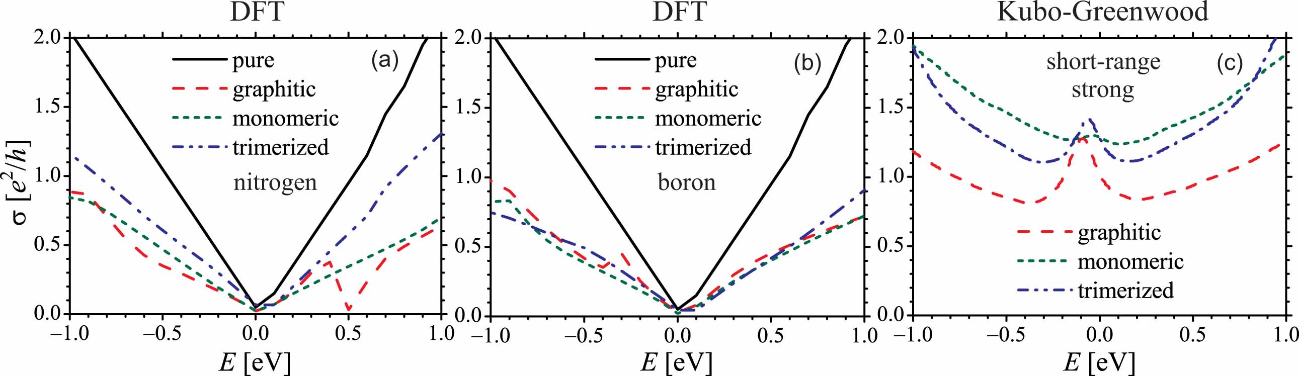
Effect of Nitrogen or Boron Doping Configurations in Graphene: DFT vs. Kubo–Greenwood Formalism
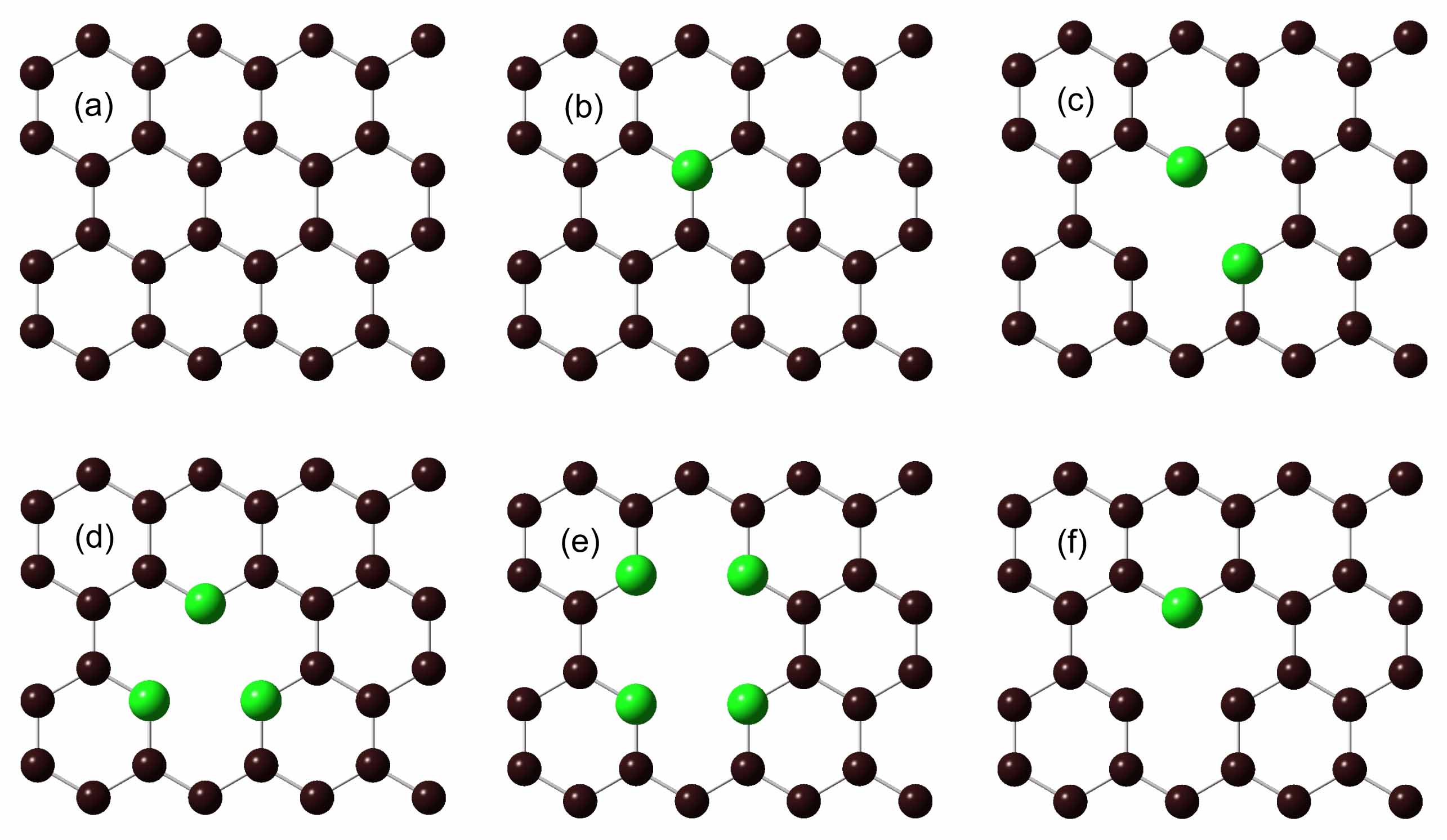
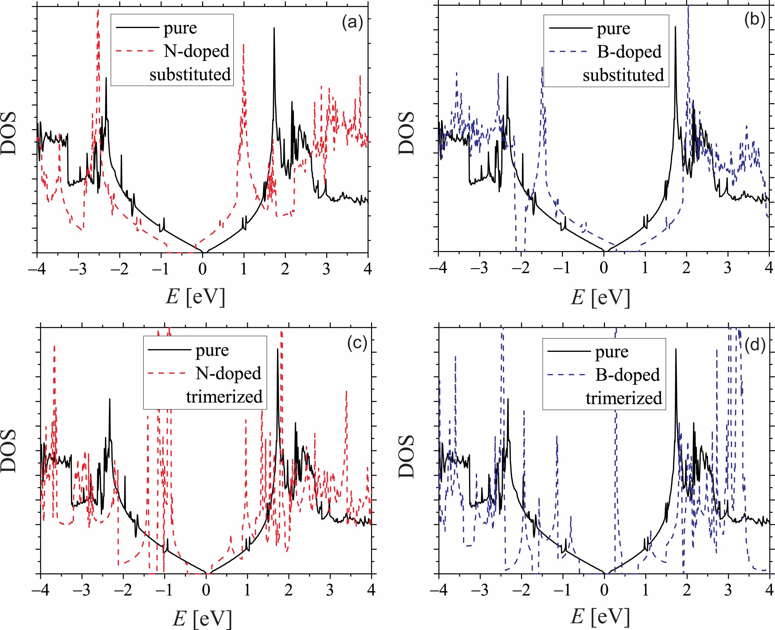
The present section deals with a comparative implementation of the above-described Kubo–Greenwood formalism and the density-functional-theory-based (DFT) method to calculate the charge transport in a B- or N-doped graphene samples. Boron and nitrogen are the most suitable and therefore commonly used substitutional dopants for incorporation into the graphene lattice. Recent experimental measurements of x-ray photoelectron spectra of N-doped nanotubes and graphene have revealed the presence of several N-doped configurations [57, 58, 59, 60]. Neglecting here the cases of topology changes in the relative positions of the honeycomb-lattice sites (i.e. line defects), there are five configurations for N- or B-doped graphene computational domain. Their geometries are illustrated in Fig. Effect of Nitrogen or Boron Doping Configurations in Graphene: DFT vs. Kubo–Greenwood Formalism. There are one graphite-type defect, N or B substitution in Fig. Effect of Nitrogen or Boron Doping Configurations in Graphene: DFT vs. Kubo–Greenwood Formalism(b), and four pyridine types of defects: dimerized in Fig. Effect of Nitrogen or Boron Doping Configurations in Graphene: DFT vs. Kubo–Greenwood Formalism(c), trimerized in Fig. Effect of Nitrogen or Boron Doping Configurations in Graphene: DFT vs. Kubo–Greenwood Formalism(d), tetramerized in Fig. Effect of Nitrogen or Boron Doping Configurations in Graphene: DFT vs. Kubo–Greenwood Formalism(e), and monomeric in Fig. Effect of Nitrogen or Boron Doping Configurations in Graphene: DFT vs. Kubo–Greenwood Formalism(f). We classify these configurations into two groups: point defects [single dopant atoms (or vacancies), as shown in Fig. Effect of Nitrogen or Boron Doping Configurations in Graphene: DFT vs. Kubo–Greenwood Formalism(b)], and complex ones containing both substitutional impurity atoms and vacancies arranged in a fixed clusters distributed over all structure [Figs. Effect of Nitrogen or Boron Doping Configurations in Graphene: DFT vs. Kubo–Greenwood Formalism(c)–(f)].
Being traditionally a powerful tool for the study of electronic and transport properties of materials, in contrast to the Kubo–Greenwood approach, the DFT method, however, does not allow to treat a large graphene systems. Here, we chose the origin graphene structure (cluster) consisting of 32 sites [Fig. Effect of Nitrogen or Boron Doping Configurations in Graphene: DFT vs. Kubo–Greenwood Formalism(a)] composing a rectangular supercell of the Å size. To exclude the interaction with other graphene sheets, the given supercell is wrapped in a vacuum of 17 Å of thickness along the -axe. The QUANTUM ESPRESSO computational packet [61] was used for calculations within the electron density functional method. To describe the exchange-correlation energy, we used the LDA approach in the Perdew–Zunger parametrization (BLYP for density of states calculation). C, N, and B atoms are described by the corresponding pseudopotentials US-PP [62]. Separation kinetic energy for the wave functions and charge densities are 30 and 300 Ry, respectively. Transport calculations are carried out using the PWCOND codes [63].
As evidenced by the DFT-based calculations of the DOS (Fig. Effect of Nitrogen or Boron Doping Configurations in Graphene: DFT vs. Kubo–Greenwood Formalism), the effect of boron and nitrogen impurities is symmetrical with respect to the Dirac point. Incorporation of boron or nitrogen atoms in substitution within the carbon matrix gives rise to the efficient - or -type doping of graphene. Oscillations in DOS for pyridine-type defects [Figs. Effect of Nitrogen or Boron Doping Configurations in Graphene: DFT vs. Kubo–Greenwood Formalism(c) and (d)] become stronger in comparison with DOS for the graphite-type defects [Figs. Effect of Nitrogen or Boron Doping Configurations in Graphene: DFT vs. Kubo–Greenwood Formalism(a) and (b)], that may be associated with a vacancy effect. Note that the oscillations, present in the DOS computed from DFT (Fig. Effect of Nitrogen or Boron Doping Configurations in Graphene: DFT vs. Kubo–Greenwood Formalism), are smoothed in the DOS from the Kubo–Greenwood approach (see DOS for random impurities in Fig. Influence of Correlated and/or Ordered Impurities on Conductivity of Graphene: Numerical Calculations) due to the significantly larger computational domain treated within the framework of the Kubo method.
Conductivity in Fig. Effect of Nitrogen or Boron Doping Configurations in Graphene: DFT vs. Kubo–Greenwood Formalism is calculated within the both DFT and Kubo–Greenwood approach, where in the latter, impurities are modeled by the short-range strong scattering potential. The DFT calculations result mainly to the linear energy dependence of the conductivity [Figs. Effect of Nitrogen or Boron Doping Configurations in Graphene: DFT vs. Kubo–Greenwood Formalism(a) and (b)], it means that electron-density dependence should be sublinear since [15, 16]. However, from the Kubo calculations, is obtained to be close to linear [see Figs. Influence of Correlated and/or Ordered Impurities on Conductivity of Graphene: Numerical Calculations(c) and Effect of Nitrogen or Boron Doping Configurations in Graphene: DFT vs. Kubo–Greenwood Formalism(c)]. Another difference is that obtained by DFT method is much more smaller than that obtained from the Kubo method. Also, results in Fig. Effect of Nitrogen or Boron Doping Configurations in Graphene: DFT vs. Kubo–Greenwood Formalism(c) are evidence of the fact that the short-range strong impurities manifest themselves as the stronger scatterers as compared with vacancy ones, but this is not the case obtained from DFT [Figs. Effect of Nitrogen or Boron Doping Configurations in Graphene: DFT vs. Kubo–Greenwood Formalism(a), (b)].
Conclusion
The statistical-thermodynamics and kinetics models of both substitutional and interstitial atomic order in the two-dimensional graphene-based crystal lattices for a wide interval of stoichiometries are constructed. Ordered distributions of substitutional and interstitial atoms over the sites and interstices of the honeycomb lattice at the different compositions and temperatures are predicted and described theoretically. The ranges of values of interatomic-interaction parameters providing the low-temperature superstructural stability are determined within the framework of both the third-nearest-neighbor Ising model and, more realistic, model taking into account interactions of all atoms present in the system at hand. The first model results in the instability of some predicted superstructures, while the second one shows that all predicted superstructures are stable at the certain values of interatomic-interaction energies. Even short-range interatomic interactions provide a stability of some graphene-based superstructures, while only long-range interactions stabilize others. Inasmuch as the intrasublattice and intersublattice interchange (mixing) energies are competitively different with the dominance of the latter, the long-range atomic order parameter(s) may relax to the equilibrium value(s) nonmonotonically.
A numerical study of electronic transport in single-layer graphene is performed by means of an efficient time-dependent real-space Kubo–Greenwood approach, which is especially suited to treat large graphene systems containing millions of atoms. The presence of neutral and/or charged point and/or line defects in graphene is modeled by various short- and long-range scattering potentials. The strong short-range scattering potential describes neutral adatoms covalently bond to graphene. The long-range Gaussian-shaped potential is appropriated for screened charged impurities on graphene and/or dielectric substrate surface. The self-consistent Thomas–Fermi approximation-based effective potential is used for charged line-acting defects (grain boundaries in CVD-grown polycrystalline graphene, atomic substrates in epitaxial graphene, etc).
Correlation in the distribution of impurity atoms gives a slight rise (up to ) in the conductivity only for the case of weak short-range potential and only if it is asymmetric (repulsive). In other the most experimentally relevant cases, namely, the short-range strong and long-range Gaussian scatterers, correlation does not affect the conductivity.
Ordering of impurities can give rise to conductivity up to tens times for weak and strong short-range scatterers as compared with the case when dopants are distributed randomly. However, as for the correlation, ordering does not affect the conductivity for the long-range-acting Gaussian potential.
Studying numerically the charge carrier transport in graphene with one-dimensional charged defects, we got electron-density dependencies of the conductivity, which showed some new features as compared with those obtained in case of point defects. First, the conductivity is found to be a robust sublinear function of electronic density and weakly dependent on the Thomas–Fermi screening wavelength. The calculated sublinear density dependence for the case of linear defects is quite different from the case of short- and long-range point scatterers, where the numerical calculations show a density dependence close to linear. We attribute the atypical, but consistent with recent experimental reports, behavior of conductivity to the extended nature of one-dimensional charged defects. Second, the conductivities of samples with different impurity geometries exhibit significant variations between each other. This is due to the fact that in contrast to point defects, the line defects are characterized not only by their positions, but also by directions (orientations) and their intersections as well. Such additional characteristics result in much more possible distributions of the potential which, in turn, leads to the differences in the conductivity curves.
The anisotropy of the conductivity along and across the line defects is revealed, which agrees with the experimental measurements for CVD graphene grown on Cu and epitaxial graphene grown on SiC. For a given concentration of the line defects, the conductivity of graphene with orientationally-correlated defects increases in comparison to the case of the uncorrelated line defects. For a given electron density, a relative increase of the conductivity for the case of fully correlated line defects in comparison to the case of uncorrelated defects is higher for a larger defect density.
A simultaneous account of both point and line defects can qualitatively and quantitatively affect the conductivity behavior in comparison with the case when only one type of them is considered. An interplay between the point and line scatterers modeled by the potential of the same sign suppresses the electron–hole asymmetry revealed if they are taken into account separately. If both point and line defects are correlated and/or ordered, it can give rise in the conductivity of graphene up to hundreds times vs. their random distribution, and thereby can serve as an additional tool to control and govern the transport properties in graphene.
Acknowledgments
T.M.R. benefited immensely from collaboration with Igor Zozoulenko, Artsem Shylau, Aires Ferreira, and appreciates discussions with Stephan Roche and Sergei Sharapov.
References
- [1] K. S. Novoselov, A. K. Geim, S. V. Morozov, D. Jiang, Y. Zhang, S. V. Dubonos, I. V. Grigorieva, and A. A. Firsov, Science 306, 666 (2004).
- [2] K. S. Novoselov, Z. Jiang, Y. Zhang, S. V. Morozov, H. L. Stormer, U. Zeitler, J. C. Maan, G. S. Boebinger, P. Kim, and A. K. Geim, Science 317, 1379 (2007).
- [3] F. Banhart, J. Kotakovski, and A. Krasheninnikov, ACS Nano 5, 26 (2011).
- [4] A. H. Castro Neto, F. Guinea, N. M. R. Peres, K. S. Novoselov, and A. K. Geim, Rev. Mod. Phys. 81, 109 (2009).
- [5] N. M. R. Peres, Rev. Mod. Phys. 82, 2673 (2010).
- [6] S. Das Sarma, S. Adam, E. H. Hwang, and E. Rossi, Rev. Mod. Phys. 83, 407 (2011).
- [7] Jun Yan and M. S. Fuhrer, Phys. Rev. Lett. 107, 206601 (2011).
- [8] Qiuzi Li, E. H. Hwang, E. Rossi, and S. Das Sarma, Phys. Rev. Lett. 107, 156601 (2011).
- [9] J. W. Klos and I.V. Zozoulenko, Phys. Rev. B 82, 081414(R) (2010).
- [10] H. Kuramochi, S. Odaka, K. Morita, S. Tanaka, H. Miyazaki, M. V. Lee, S.-L. Li, H. Hiura, and K. Tsukagoshi, AIP Advances 2, 012115 (2012).
- [11] S. Günther, S. Dänhardt, B. Wang, M.-L. Bocquet, S. Schmitt, and J. Wintterlin, Nano Lett. 11, 1895 (2011).
- [12] Ch. Held, T. Seyller, and R. Bennewitz, Beilstein J. Nanotechnol. 3, 179 (2012).
- [13] G.-X. Ni, Yi Zheng, S. Bae, H. Ri Kim, A. Pachoud, Y. S. Kim, C.-L. Tan, D. Im, J.-H. Ahn, B. H. Hong, and B. Özyilmaz, ACS Nano 6, 1158 (2012).
- [14] M. K. Yakes, D. Gunlycke, J. L. Tedesco, P. M. Campbell, R. L. Myers-Ward, Ch. R. Eddy, Jr., D. K. Gaskill, P. E. Sheehan, and A. R. Laracuente, Nano Lett. 10, 1559 (2010).
- [15] T. M. Radchenko, A. A. Shylau, and I. V. Zozoulenko, Phys. Rev. B 86, 035418 (2012).
- [16] T. M. Radchenko, A. A. Shylau, I. V. Zozoulenko, and A. Ferreira, Phys. Rev. B 87, 195448 (2013).
- [17] A. G. Khachaturyan, Theory of Structural Transformations in Solids, Dover Publications, Minola, NY, 2008.
- [18] T. M. Radchenko and V. A. Tatarenko, Nanosistemi, Nanomateriali, Nanotehnologii (Nanosystems, Nanomaterials, Nanotechnologies) 6, 867 (2008) (in Ukrainian).
- [19] T. M. Radchenko, Metallofizika i Noveishie Tekhnologii 30, 1021 (2008).
- [20] T. M. Radchenko and V. A. Tatarenko, Solid State Phenomena 150, 43 (2009).
- [21] T. M. Radchenko and V. A. Tatarenko, Physica E 42, 2047 (2010).
- [22] T. M. Radchenko and V. A. Tatarenko, Int. J. Hydrogen Energy 36, 1338 (2010).
- [23] T. M. Radchenko and V. A. Tatarenko, Solid State Sciences 12, 204 (2010).
- [24] I. Yu. Sagalianov, T. M. Radchenko, Yu. I. Prylutskyy, and V. A. Tatarenko, Uspehi Fiziki Metallov (Progress in Physics of Metals) 11, 95 (2010) (in Ukrainian).
- [25] V. N. Bugaev and V. A. Tatarenko, Interaction and Arrangement of Atoms in Interstitial Solid Solutions Based on Close-Packed Metals, Naukova Dumka, Kiev, 1989 (in Russian).
- [26] T. M. Radchenko and V. A. Tatarenko, Nanosistemi, Nanomateriali, Nanotehnologii (Nanosystems, Nanomaterials, Nanotechnologies) 8, 619 (2010) (in Ukrainian).
- [27] D. V. Tuan, J. Kotakoski, T. Louvet, F. Ortmann, J. C. Meyer, and S. Roche, Nano Lett. 13, 1730 (2013).
- [28] S. Roche, N. Leconte, F. Ortmann, A. Lherbier, D. Soriano, and J.-Ch. Charlier, Solid State Comm. 153, 1404 (2012).
- [29] T. Markussen, R. Rurali, M. Brandbyge, and A.-P. Jauho, Phys. Rev. B 74, 245313 (2006); T. Markussen, Master thesis, Technical University of Denmark, 2006.
- [30] S. Yuan, H. De Raedt, and M. I. Katsnelson, Phys. Rev. B 82, 115448 (2010).
- [31] N. Leconte, A. Lherbier, F. Varchon, P. Ordejon, S. Roche, and J.-C. Charlier, Phys. Rev. B 84, 235420 (2011).
- [32] A. Lherbier, S. M.-M. Dubois, X. Declerck, Y.-M. Niquet, S. Roche, and J.-Ch. Charlier, Phys. Rev. B 86, 075402 (2012).
- [33] H. Ishii, N. Kobayashi, and K. Hirose, Phys. Rev. B 82, 085435 (2010).
- [34] J. P. Robinson, H. Schomerus, L. Oroszlany, and V. I. Fal’ko, Phys. Rev. Lett. 101, 196803 (2008).
- [35] T. O. Wehling, S. Yuan, A. I. Lichtenstein, A. K. Geim, and M. I. Katsnelson, Phys. Rev. Lett. 105, 056802 (2010).
- [36] S. Ihnatsenka and G. Kirczenow, Phys. Rev. B 83, 245442 (2011).
- [37] A. Ferreira, J. Viana-Gomes, J. Nilsson, E. R. Mucciolo, N. M. R. Peres, A. H. Castro Neto, Phys. Rev. B 83, 165402 (2011).
- [38] O. Madelung, Introduction to Solid-State Theory, Springer, Berlin, 1996.
- [39] K. S. Kim, Y. Zhao, H. Jang, S. Y. Lee, J. M. Kim, K. S. Kim, J. H. Ahn, P. Kim, J. Y. Choi, and B. H. Hong, Nature 457, 706 (2009).
- [40] W. A. de Heer, C. Berger, X. Wu, P. N. First, E. H. Conrad, X. Li, T. Li, M. Sprinkle, J. Hass, M. L. Sadowski, M. Potemski, and G. Martinez, Solid State Comm. 143, 92 (2007).
- [41] B. W. Jeong, J. Ihm, and G.-D. Lee, Phys. Rev. B 78, 165403 (2008).
- [42] O. V. Yazyev and S. G. Louie, Phys. Rev. B 81, 195420 (2010).
- [43] S. Malola, H. Hakkinen, and P. Koskinen, Phys. Rev. B 81, 165447 (2010).
- [44] A. Ferreira, X. Xu, C.-L. Tan, S.-K. Bae, N. M. R. Peres, B.-H. Hong, B. Ozyilmaz, and A. H. Castro Neto, Eur. Phys. Lett., 94, 28003 (2011).
- [45] C. Dimitrakopoulos, A. Grill, T. McArdle, Z. Liu, R. Wisnieff, and D. A. Antoniadis, Appl. Phys. Lett. 98, 222105 (2011).
- [46] S.-H. Ji, J. B. Hannon, R. M. Tromp, V. Perebeinos, J. Tersoff, and F. M. Ross, Nature Mater. 11, 114 (2012).
- [47] Y. M. Lin, D. B. Farmer, K. A. Jenkins, Y. Wu, J. L. Tedesco, R. L. Myers-Ward, C. R. Eddy, D. K. Gaskill, C. Dimitrakopoulos, and P. Avouris, IEEE Electron Device Lett., 32, 1343 (2011).
- [48] T. Low, V. Perebeinos, J. Rersoff, and Ph. Avouris, Phys. Rev. Lett. 108, 096601 (2012).
- [49] O. V. Yazyev and S. G. Louie, Nat. Mater. 9, 806 (2010).
- [50] L. Jiang, G. Yu, W. Gao, Z. Liu, and Y. Zheng, Phys. Rev. B 86, 165433 (2012)
- [51] J. N. B. Rodrigues, N. M. R. Peres, and J. M. B. Lopes dos Santos, Phys. Rev. B 86, 214206 (2012).
- [52] H. Xu, T. Heinzel, and I. V. Zozoulenko, Phys. Rev. B 84, 115409 (2011).
- [53] H. S. Song, S. L. Li, H. Miyazaki, S. Sato, K. Hayashi, A. Yamada, N. Yokoyama, and K. Tsukagoshi, Sci. Rep. 2, 337 (2012).
- [54] A. W. Tsen, L. Brown, M. P. Levendorf, F. Ghahari, P. Y. Huang, R. W. Havener, C. S. Ruiz-Vargas, D. A. Muller, Ph. Kim, and J. Park, Nature 467, 305 (2010).
- [55] J. P. Robinson, H. Schomerus, L. Oroszlany, and V. I. Fal’ko, Phys. Rev. Lett. 101, 196803 (2008).
- [56] T. O. Wehling, S. Yuan, A. I. Lichtenstein, A. K. Geim, and M. I. Katsnelson, Phys. Rev. Lett. 105, 056802 (2010).
- [57] D. Wei, Y. Liu, Y. Wang, H. Zhang, L. Huang, and G. Yu, Nano Lett. 9, 1752 (2009).
- [58] Y.-C. Lin, C.-Y. Lin, and P.-W. Chiu, Appl. Phys. Lett. 96, 133110 (2010).
- [59] P. Ayala, A. Grüneis, T. Gemming, D. Grimm, C. Kramberger, M. H. Rümmeli, L. Freire Jr., H. Kuzmany, R. Pfeiffer, A. Barreiro, B. Büchner, and T. Pichler, J. Phys. Chem. C 111, 2879 (2007).
- [60] B. Guo, Q. Liu, E. Chen, H. Zhu, L. Fang, and J. R. Gong, Nano Lett. 10, 4975 (2010).
- [61] P. Giannozzi, S. Baroni, N. Bonini, M. Calandra, R. Car, C. Cavazzoni, D. Ceresoli, G.L. Chiarotti, M. Cococcioni, I. Dabo, A. Dal Corso, S. de Gironcoli, S. Fabris, G. Fratesi, R. Gebauer, U. Gerstmann, C. Gougoussis, A. Kokalj, M. Lazzeri, L. Martin-Samos, N. Marzari, F. Mauri, R. Mazzarello, S. Paolini, A. Pasquarello, L. Paulatto, C. Sbraccia, S. Scandolo, G. Sclauzero, A.P. Seitsonen, A. Smogunov, P. Umari, and R. M. Wentzcovitch, J. Phys.: Condens. Matter. 21, 395502 (2009).
- [62] We used pseudopotentials C.pz-vbc.UPF, B.pz-vbc.UPF, N.pz-vbc.UPF, C.blyp-van_ak.UPF, N.blyp-van_ak.UPF, B.blyp-n-van_ak.UPF at http://www.quantum-espresso.org.
- [63] A. Smogunov, A. Dal Corso, and E. Tosatti, Phys. Rev. B 70, 045417 (2004).