Contactless Measurement of AC Conductance in Quantum Hall Structures
Abstract
We report a procedure to determine the frequency-dependent conductance of quantum Hall structures in a broad frequency domain. The procedure is based on the combination of two known probeless methods – acoustic spectroscopy and microwave spectroscopy. By using the acoustic spectroscopy, we study the low-frequency attenuation and phase shift of a surface acoustic wave in a piezoelectric crystal in the vicinity of the electron (hole) layer. The electronic contribution is resolved using its dependence on a transverse magnetic field. At high frequencies, we study the attenuation of an electromagnetic wave in a coplanar waveguide. To quantitatively calibrate these data, we use the fact that in the quantum-Hall-effect regime the conductance at the maxima of its magnetic field dependence is determined by extended states. Therefore, it should be frequency independent in a broad frequency domain. The procedure is verified by studies of a well-characterized -SiGe/Ge/SiGe heterostructure.
pacs:
73.23.b, 73.50.RbI Introduction
The dynamics of charge carriers in low-dimensional quantum structures has been in the focus of interest for many years. A special role in its study is played by probeless methods allowing the influence of contacts to be avoided.
In one of these methods the attenuation and the phase shift of a surface acoustic wave (SAW) are measured. These are caused by charge carriers in a two-dimensional (2D) layer located close to the surface supporting the SAW. To the best of our knowledge, the first results of acoustic studies of 2D electron systems were reported in Ref. Wixforth1986, . In that paper, the interaction of a SAW with the 2D electrons in a GaAs/AlGaAs heterostructure was investigated in the integer quantum Hall effect (IQHE) regime. In this work, a SAW was excited and propagated directly on the surface of a piezoelectric GaAs/AlGaAs sample. This procedure caused the sample to be somewhat mechanically stressed and thereby deformed. Later the authors suggested a configuration in which no mechanical deformation is transferred from the piezoelectric substrate to the sample, such that only the electrical field matters. Wixforth1989 This allowed to determine the complex AC conductance, , from the measured SAW attenuation and phase shift. A relevant theoretical model developed in Refs. Efros1990, ; Simon1996, ; Kagan1997, allowed extracting quantitative information, as was shown in subsequent works. Drichko2000 ; Drichko2005 ; Drichko2008 ; Drichko2009 ; Drichko2013 However, the acoustic method has an upper frequency limit,associated with technological problems in producing the inter-digital transducers (IDTs) used for the excitation and detection of the SAW, see Sec. II.2.1.
At the same time, measurements of the electron response in low-dimensional systems to high-frequency perturbations are especially important, as being related to several intrinsic properties of low-dimensional systems. Among these properties are peculiarities of electron localization, collective modes and their pinning, mechanisms of integer and fractional quantum Hall effects, etc. A powerful approach is provided by microwave spectroscopy (MWS) suggested in Ref. Engel1993, . Various modifications of this method, including probeless ones, were developed in Refs. Stone2012, ; Endo2013, ; Chen_thesis, ; Stone_thesis, . The MWS provides a much broader frequency domain compared with acoustic spectroscopy (AS) - from hundreds of megahertz to dozens of gigahertz. It is very efficient for studying the dependence of the electron response on magnetic field, temperature, etc. However, it is rather difficult to calibrate the measured AC conductance in absolute units, which is why the results of many papers on this subject are presented in relative units.
The aim of the present work is to compare the results of microwave measurements of with those obtained using AS, as well as DC transport measurements. This comparison will facilitate the calibration of the dynamical electromagnetic response of the low-dimensional electron gas in absolute units.
II Experiment
II.1 Sample
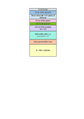
Since it is very important to use well-characterized samples we have chosen the p-SiGe/Ge/SiGe heterostructure (K6016) investigated earlier in Refs. Drichko2009, ; Drichko2013, by means of AS. The structure of the sample is schematically shown in Fig. 1. The sample was made by low-energy plasma-enhanced chemical vapor deposition (LEPECVD), see lepecvd for details. The active part of the sample is a 2D hole channel formed in a strained Ge layer. The density and mobility of holes are cm-2 and cm2/(V s), respectively, at 4.2 K.
II.2 Experimental methods
In the following, we briefly explain the two methods employed for the AC conductance measurements - one (AS) based on the propagation of the SAWs and the other on microwave spectroscopy (MWS).
II.2.1 Acoustic spectroscopy
In Fig. 2 is shown a sketch of the acoustic method.
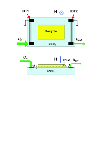
A SAW is excited on the surface of a piezoelectric LiNbO3 crystal by electromagnetic pulses applied to an interdigital transducer IDT1 and detected by another interdigital transducer IDT2 placed on the same surface. The SAW, generated by the piezoelectric effect in LiNbO3, is accompanied by a travelling electromagnetic wave. The sample is pressed onto the surface by a spring. As a result, the electric field of the travelling wave penetrates into the 2D hole gas and interacts with holes. This interaction leads to an attenuation, , and a phase shift of the SAW, both of which are measured. The latter manifests itself as a renormalization of the SAW phase velocity, . It is important to note that both real and imaginary parts of the conductance vanish in a strong perpendicular magnetic field. This creates the possibility to single out the electron contribution by subtracting the zero-field values of and from those in a strong magnetic field. The expressions for these differences, as well as the parameters which we use for finding the conductances, are given in Appendix A as Eqs. (5) and (6). They are based on the derivation given in Ref. Kagan1997, .
II.2.2 Microwave spectroscopy
In Fig. 3 is shown a sketch of the experimental setup for microwave spectroscopy. In this case, the sample is placed on a meandered coplanar waveguide (CPW) formed on the surface of an insulating GaAs substrate. The microwave pulses applied to the CPW center conductor excite a quasi-transverse electromagnetic mode (quasi-TEM mode). Similarly to the case of a SAW, the interaction with holes in the 2D layer leads to the attenuation of this mode, as well as to a change of its phase. Again, both effects are due to the complex conductance of the 2D layer. To separate these contributions, we will subtract the results in a transverse magnetic field from the zero-field ones.
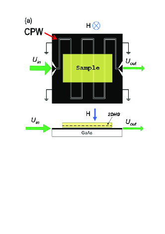
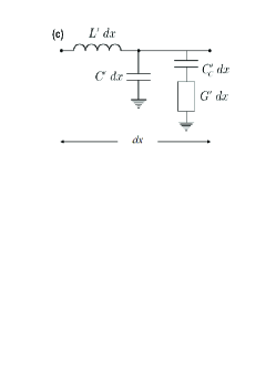
To relate the measurable quantities with the complex conductance, a simple transmission line model is used as outlined in Fig. 3c. Here is the inductance of the center conductor per unit length and the capacitance between the center conductor and ground (side plane) per unit length. The 2D layer constitutes a shunt admittance from the CPW center conductor to the ground. is the capacitance per unit length from the center conductor (of width ) to the 2D layer (located at a distance below the surface), where is the capacitance per unit area. If , the microwave electric field is mainly confined in the slots, and the shunt capacitance ( term) has a negligible contribution compared to that of the shunt conductance ( term, where is the conductance per unit length of the 2D layer under both slots (thus the factor of 2)). In this case, the CPW simply acts as contacts to the 2D hole layer. Here is the conductance in the direction of the electric field.
The wave attenuation is given as Simons ; Chen_thesis :
| (1) |
Substituting the expressions for , and (given, e.g., by Eqs. (D.1)-(D.3) in Appendix D of Chen_thesis ,), we can express through the attenuation coefficient, . This expression can be cast in the form (cf. with Endo2013 ):
| (2) |
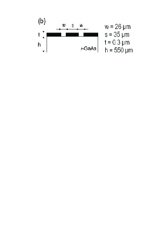
Here is the phase velocity of the wave, - is the vacuum velocity of light, is the dielectric constant of -GaAs, and is the characteristic impedance. In our experiment the parameters of the CPW are selected in order to have m/s and Ohm, see Fig. 3.
Equation (2) is valid under the following conditions Engel1993 : (i) There are no reflections at the CPW edges; (ii) The AC current is concentrated inside the slots, i. e., the width of the slot, , should exceed the wave penetration depth in the stripes. The inequality can be written as
| (3) |
Here is the capacitance between the metallic grounded stripe and the 2D layer per unit area, F/m is the vacuum permittivity, is the clearance between the sample and the -GaAs surface; =1 and =16.2 are the dielectric constants, of vacuum, and of the semiconductor, respectively. Putting m and m, we get F/m2. Then the inequality (3) can be rewritten as
| (4) |
where we have substituted m. The inequality (4) is a serious limitation for the quantitative determination of for samples with relatively large conductance. Therefore, one should be careful while extracting quantitative information from electromagnetic measurements, especially at relatively low frequencies. In what follows we will report our procedure for extracting in a broad frequency domain by combining the results of acoustic and electromagnetic measurements.
III Results
III.0.1 Acoustic spectroscopy
Acoustic spectroscopy is most suitable for low frequencies, the upper frequency limit being mainly defined by design of the IDT. Shown in Fig. 4 are magnetic field dependences of the attenuation, (a), and the SAW velocity, (b) at a frequency MHz and temperature K. The filling factors are shown by arrows.
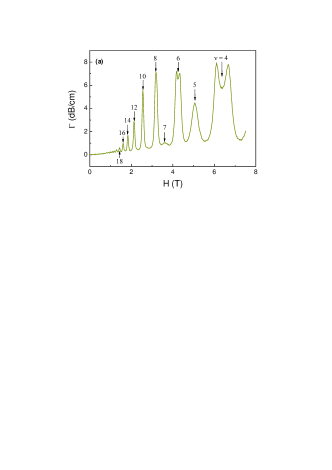
Using the procedure based on the expressions given in Appendix A and described in detail in Drichko2000 ; Drichko2008 ; Drichko2013 , we can extract both the real and imaginary parts of the complex AC conductance. The extracted magnetic field dependence of is shown in Fig. 4c.
III.0.2 Microwave spectroscopy
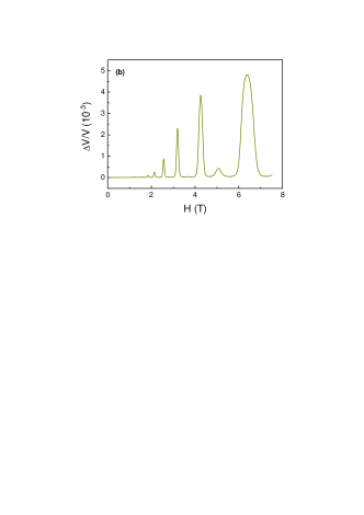
Shown in Fig. 5a is the magnetic field dependence of the output signal, of the CPW at a frequency of 1102 MHz and a temperature of 1.7 K. The sample is the same as that used for the acoustic measurements.
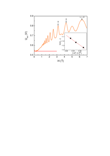
To relate the output signal to the sample conductance, one also needs to know the input signal, . This is not a trivial task since we observed a significant background signal independent of the magnetic field. We attribute this signal to some leakage in the structure and present the total output signal as . Here is the signal having interacted with the sample, while (shown by solid red line in Fig. 5) represents the leakage. According to our measurements, the magnetic field dependence of the phase shift of the total output signal is relatively weak, the field-dependent shift being 20-50∘. Therefore, we simply subtract the background amplitude, i.e. , from the total output amplitude.
Now we take into account that the oscillations of versus magnetic field are caused by oscillations of the diagonal conductance in the regime of the integer quantum Hall effect. As is well known, the maxima of the diagonal conductance correspond to extended states close to the Landau level centers. At the same time, the wave frequencies are much below that the typical electron relaxation rate, . Therefore, one can expect that the maximal values of the AC conductance should coincide with the values of the static conductance at the same magnetic field. This is illustrated in Fig. 4c.
At the same time, the minima of the AC conductance in the IQHE regime are determined by hopping between localized states, see, e. g., Ref.Polyakov1993, and references therein. The hopping AC conductance is also suppressed by an external transverse magnetic field, and in strong magnetic fields (with logarithmic accuracy), see, e.g., Ref.Galperin1991-review, . This dependence is experimentally confirmed, and we use it to find . An example including 3 signal maxima or conductance minima, corresponding to the filling factors is shown in the inser of Fig. 5a (inset), where we have plotted versus . The intercept of the straight line fit with the ordinate axis provides the value of corresponding to V. Knowing , we then find the real part of the conductance from Eq. (2).
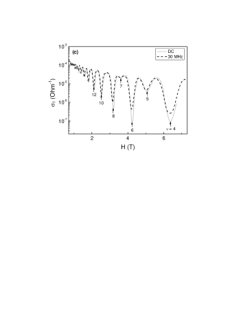
The results for obtained by AS for MHz and MWS for MHz are shown in Fig. 6a.
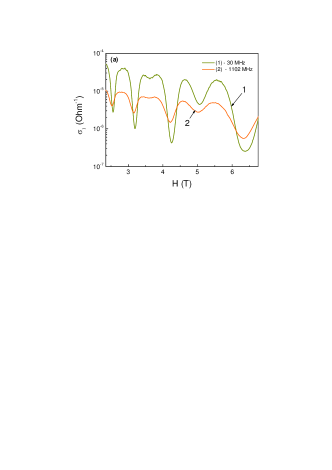
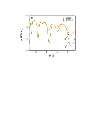
According to our estimates, the inequality (4) needed for the validity of Eq. (2) is met only within an order of magnitude. Therefore, it is hard to expect high numerical accuracy of the values of extracted from the CPW measurements. However, we know that at the maxima of the curves the conductance should coincide with the static one for any frequency, so they should be frequency-independent. Therefore, we suggest rescaling the curve by some factor, , such that the values of at the maxima will be equal to the static conductance, , for the same temperature. The results of low-frequency acoustic measurements do not need such rescaling since, as shown in Fig. 6c, is the required frequency independence of the maxima is fulfilled automatically. The result of such rescaling for MWS at MHz is shown in Fig. 6b. The scale factor turns out to be .
At the same time, the values of at the minima are strongly depend on frequency. This is natural, because a hopping transport mechanism is valid for magnetic field values far from the maxima of , which inevitably depends on frequency. Based on the above considerations, we use the following procedure to analyze at the conductance minima: (i) For each frequency and temperature, after subtracting the -independent background , we determine the input signal, , using the procedure described earlier; (ii) Then we determine using Eq. (2); (iii) After that we rescale the data by some factor determined in such a way that the maxima coincide with those obtained from either acoustic or DC measurements.
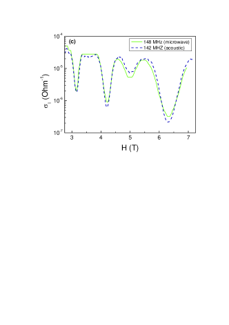
To verify the suggested procedure, we applied it to both AS and MWS for closely similar frequencies. The result is shown in Fig. 6c. Since the frequencies are close, the curves should coincide. This can indeed be seen to be the case, such that our can be considered consistent.
III.0.3 Frequency dependence of AC conductance
In Fig. 7 are shown the magnetic field dependences of for different frequencies. They are obtained using the procedure outlined in Sec. III.0.2. The insert shows the frequency dependence of the scaling factor .
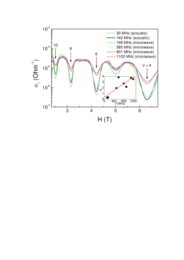
The frequency dependence of the conductance in the minima with and at K is shown in Fig. 8.
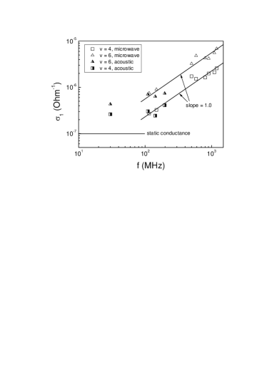
It is clear that at sufficiently high frequencies, MHz, the minimal values of are roughly proportional to , as it should be for AC hopping conductance. The solid line shows the value of the static conductance, . At very low frequencies, the two-site model leading to dependence is not applicable, and more complicated clusters become important, see for a review Refs. Efros1985, ; Dyre2000, . As a result, . This might be the reason of the fact that the point corresponding to MHz falls above the line corresponding to the slope of 1 in the vs. dependence.
IV Discussion and conclusions
We have developed a procedure for quantitative probeless measurements of the AC conductance of 2D electron/hole layers in a broad frequency domain. The main ingredient of this procedure is to measure the attenuation of surface acoustic waves (at low frequencies) and electromagnetic modes in the CPW (at high frequencies) in a transverse magnetic field in the regime of the IQHE. Since the transverse magnetic field suppresses the electronic contribution to the conductance both in diffusive and hopping regimes, it is possible to resolve the contribution of the charge carriers.
Another important point is to rescale the data obtained by MWS such that the maxima of for all frequencies coincide with the static conductance (and with the results of low-frequency acoustic measurements). This rescaling to some extent compensates for the leakage of the electromagnetic modes outside the slots of the CPW. The results of acoustic measurements do not need such rescaling since the maxima of for all SAW frequencies coincide with those of the static conductance. This fact allows avoiding DC measurements which would require contacts. On the other hand, extracted from MWS for any frequency can be rescaled to make the maxima coinciding with those extracted from AS. In this way, we can determine in a broad domain of frequencies and magnetic fields without the need of contacts. This is the main conclusion of this work.
The suggested procedure has been tested using a well-characterized sample. It is shown that at frequencies close to 150 MHz, where both the AS and MWS can be performed, the dependences obtained by both spectroscopies practically coincide with each other.
The advantage of the procedure is that it can be applied to various materials and structures. In particular, systems without intrinsic piezoelectric effect can be studied acoustically since the sample is mounted on the surface of a piezoelectric crystal. The procedure is especially useful for studies of the AC conductance in the hopping regime, which is the case in the minima of the IQHE.
Acknowledgements.
This work was supported by Russian Foundation for Basic Research grant of RFBR 14-02-0023214, Presidium of the Russian Academy of Science, the U.M.N.I.K grant 16906, and, partially, from Era.Net-Rus.Appendix A Expressions for sound absorption and velocity
| (5) | |||
| (6) |
where
| (7) |
is the SAW wave vector, is the depth of the 2D-system layer in the sample, is the clearance between the sample and the LiNbO3 surface; =50, =1 and =11.7 are the dielectric constants of LiNbO3, of vacuum, and of the semiconductor, respectively.
References
- (1) A. Wixforth, J. P. Kotthaus, and G. Weimann, Phys. Rev. Lett. 56, 2104 ( 1986).
- (2) A. Wixforth, J. Scriba, M. Wassermeier, J. P. Kotthaus, G. Weimann, and W. Schlapp, Phys. Rev. B 40, 7874 ( 1989).
- (3) A. L. Efros and Y. M. Galperin, Phys. Rev. Lett. 64, 1959 ( 1990).
- (4) S. H. Simon, Phys. Rev. B 54, 13878 ( 1996).
- (5) V. D. Kagan, Semiconductors 31, 407 ( 1997).
- (6) I. L. Drichko, A. M. Diakonov, I. Y. Smirnov, Y. M. Galperin, and A. I. Toropov, Phys. Rev. B 62, 7470 ( 2000).
- (7) I. L. Drichko, A. M. Diakonov, I. Y. Smirnov, G. O. Andrianov, O. A. Mironov, M. Myronov, D. R. Leadley, and T. E. Whall, Phys. Rev. B 71, 045333 ( 2005).
- (8) I. L. Drichko, A. M. Dyakonov, I. Y. Smirnov, A. V. Suslov, Y. M. Galperin, V. Vinokur, M. Myronov, O. A. Mironov, and D. R. Leadley, Phys. Rev. B 77, 085327 ( 2008).
- (9) I. L. Drichko, A. M. Diakonov, E. V. Lebedeva, I. Y. Smirnov, O. A. Mironov, M. Kummer, and H. von Känel, J. Appl. Phys. 106, 094305 ( 2009).
- (10) I. L. Drichko, V. A. Malysh, I. Y. Smirnov, A. V. Suslov, O. A. Mironov, M. Kummer, and H. von Känel, J. Appl. Phys. 114, 074302 ( 2013).
- (11) L. W. Engel, D. Shahar, Ç. Kurdak, and D. C. Tsui, Phys. Rev. Lett. 71, 2638 ( 1993).
- (12) K. Stone, R. R. Du, M. J. Manfra, L. N. Pfeiffer, and K. W. West, Appl. Phys. Lett. 100, 192104 ( 2012).
- (13) A. Endo, T. Kajioka, and Y. Iye, Journ. Phys. Soc. Jpn 82 ( 2013).
- (14) Y. P. Chen, Quantum solids of two dimensional electrons in magnetic fields, Ph.D. thesis, Princeton University ( 2005).
- (15) K. J. Stone, Millimeter wave transmission spectroscopy of 2D electron and hole systems, Ph.D. thesis, Rice University ( 2010), p. 46.
- (16) C. Rosenblad, H.R. Deller, A. Dommann, T. Meyer, P. Schroeter, and H. von Känel, J. Vac. Sci. Technol. A 16, 2785 (1998).
- (17) R. N. Simons, Coplanar Waveguide, Circuits, Components, and Systems ( Wiley-Interscience, New York, Chichester, Weinheim, Brisbane, Singapore, Toronto, 2001).
- (18) D. G. Polyakov and B. I. Shklovskii, Phys. Rev. B 48, 11167 ( 1993).
- (19) Y. M. Galperin, V. L. Gurevich, and D. A. Parshin, “ Non-Ohmic Microwave Hopping Conductivity,” in Hopping Transport in Solids, edited by M. Pollak and B. Shklovskii ( Elsevier Science Publishers B.V., Amsterdam, 1991).
- (20) A.L. Efros and B.I. Shklovskii, in Electron-Electron Interactions in Disordered Systems, edited by A. L. Efros and M. A. Pollak ( North-Holland, Amsterdam, 1985) p. 201.
- (21) J. C. Dyre and T. B. Schrøder, Rev. Mod. Phys. 72, 873 (2000).