High Quantum Efficiency Ultrananocrystalline Diamond
Photocathode:
Negative Electron Affinity Meets -doping
Abstract
We report results of quantum efficiency (QE) measurements carried out on a 150 nm thick nitrogen-incorporated ultrananocrystalline diamond terminated with hydrogen; abbreviated as (N)UNCD:H. (N)UNCD:H demonstrated a QE of 10-3 (0.1%) at 254 nm. Moreover, (N)UNCD:H was sensitive in visible light with a QE of 510-8 at 405 nm and 510-9 at 436 nm. After growth and prior to QE measurements, samples were exposed to air for about 2 hours for transfer and loading. Such design takes advantage of a key combination: 1) H-termination inducing negative electron affinity (NEA) on the (N)UNCD and stabilizies its surface against air exposure; and 2) N-incorporation inducing -type conductivity in intrinsically insulating UNCD.
The photocathode is a key component of the electron injectors in synchrotrons, free electron lasers, linear accelerators (linacs), and ultrafast electron systems for imaging and diffraction. Choice of a specific photocathode is application specific, and there is always a trade-off: QE vs. lifetime/robustness vs. response time vs. emittance. It is generally accepted that if a technology providing a high QE photocathode operating at moderate vacuum conditions existed, it would greatly benefit the field of photoinjectors R&D.1
Semiconductor photocathodes still hold records in terms of QE. These are low work function (WF) alkali/multialkali based materials that are used in a form of thin films to absorb light and emit electrons,2 ; 3 or in a form of ultrathin layers to activate traditional metal photocathodes.4 Activation of heavily doped -Si or -GaAs surfaces with alkali Cs has led to a special photocathode type with negative electron affinity (NEA). NEA is a unique circumstance, when electrons injected to the conduction band can be emitted directly into the vacuum. Such NEA photocathodes are bright electron sources because of their high QE and low emittance, which decreases as the NEA value increases.5 The NEA value is a measure of how the low vacuum level locates with respect to conduction band minimum. Nevertheless, the main drawback of alkali-based photocathodes remains the same – they require a vacuum base pressure 10-10 Torr for synthesis, handling and operation.
Wide bandgap (5 eV) semiconductors are another class of NEA materials. This includes AlN, BN, and diamond.6 ; 7 In diamond, NEA can be either an inherent surface property8 or an engineered one9 via surface treatment in a hydrogen environment. Since the first experiment which demonstrated a remarkable quantum yield from a NEA diamond surface under vacuum UV illumination,8 prototypes of solar blind high efficiency photocathodes for space research detectors have been introduced.10 High purity H-terminated synthetic diamond has been found to be an excellent electron amplifier, where the primary electrons from a standard QE photocathode (e.g. Cu) accelerated to a keV energy get multiplied upon transmission through a thin diamond film. Chang et al.11 have demonstrated gain coefficients as high as 200. In most previous applications, high purity (no dopants) diamonds or boron doped (-type conductivity) diamonds were used. Thus vacuum UV wavelengths (200 nm) were targeted. Boron -doping did not play a significant role12 as the boron level is only 0.4 eV above the top of the valence band in diamond.
To take advantage of NEA and sensitize diamond towards the near UV and visible spectral ranges, and thus make it of interest to the photoinjectors R&D community, one should introduce electrons in diamond. A way to do so would be -doping. Relatively recent progress in -doping of micro-, nano- and ultranano-crystalline diamond offers a few options: sulfur (activation energy, , 0.4 eV13 ), phosphorous (=0.6 eV14 ), and nitrogen (=1.7 eV15 ). Given that the electron affinity promoted by hydrogen can be as low as –1 eV (NEA value=1 eV),16 all aforementioned dopants are capable of promoting visible light photo-excitation. To date, there is one report experimentally showing that (N)UNCD:H is sensitive to the visible range. Sun et al.17 reported a measurable external quantum effect at room temperature between 400 and 480 nm; but no QE values were presented. With this letter, we report proof-of-concept QE measurements suggesting that -doped UNCD:H is an emergent air resistant NEA photocathode for photoinjectors. QE measurements were carried out in the near UV range 250-270 nm, standard for many photocathode applications, and in visible light at 405 and 436 nm. The cathode was exposed to air for about 2 hours for transfer and loading; QE was measured at base pressure 10-6 Torr.
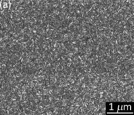
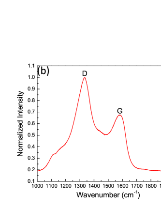
(N)UNCD films were synthesized on a polycrystalline molybdenum substrate in a 915 MHz microwave-assisted plasma chemical vapor deposition (MPCVD) reactor (Lambda Technologies Inc.) Growth of UNCD on foreign substrates requires a nanodiamond (ND) pre-seeding treatment prior to deposition to promote growth in the MPCVD. Slurry of ND particles from Adámas Technologies was used. The average particle size of the seeds was 5-10 nm. Mo substrates were immersed into the ND slurry and subject to ultrasonic treatment in the solution for 20 minutes. Subsequent growth of the (N)UNCD films was under following conditions: substrate temperature 850 ∘C; operation chamber pressure 56 Torr; microwave power 2.3 kW; individual gas flows in the precursor gas mixture were 3 sccm CH4/160 sccm Ar/40 sccm N2. Fig.1a shows a scanning electron micrograph of a deposited film taken by an FEI Nova 600 NanoLab. A uniform microstructure, typical for UNCD, was observed. Fig.1b represents a Raman spectrum recorded by a Renishaw InVia Raman Microscope using a 633 nm laser line. The shoulder around 1140 cm-1 corresponds to the (C-H in-plain bending) vibrational mode of trans-polyacetylene and the shoulders at 1340 and 1540 cm-1 correspond to the D and G bands of diamond, respectively.18 ; 19 The films had a conductivity comparabale with that of Mo substrates. As a final step, the samples underwent to H-termination procedure for 15 minutes. It was accomplished in the same MPCVD reactor at substrate temperature of 750 ∘C. H2 gas flow was 200 sccm at chamber pressure 15 Torr, and the microwave power was 2 kW. After that, the samples were left to cool down to room temperature naturally.
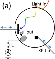
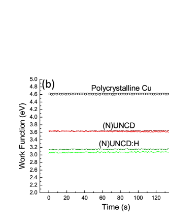
Measurements of the synthesized samples were performed in a commercial Kelvin probe (KP) instrument (KP6500 from McAllister Technical Service) with custom in-house modifications so that the WF and QE can be obtained in the same experimental run. Before or after termination, all samples were taken from the synthesis chamber and transported to the KP under ambient conditions; total exposure time was about 2 hours. The KP chamber in all measurements was evacuated to a base pressure of 10-6 Torr. Fig.2a represents a cartoon of the experimental setup. A voltage of +300 V was applied to a small aluminum anode plate, and a current of photoelectrons to the ground was collected by the same source/ammeter (Keithley 6487) with a threshold sensitivity of 10 fA. The anode plate was introduced into a KP chamber at an angle such that it is does not interfere with light beam and a tip assessing WF. A sample holder actuator and the KP tip are both retractable, and ideal positions can be found for QE and WF measurements independently. WFs for (N)UNCD samples were determined by KP with respect to its calibrated tip (WF=4.6 eV) before and after they underwent H-plasma treatment. A sample holder made of standard polycrystalline copper was used as a reference. All deduced WF values are plotted in Fig.2b. WF dependence on time is a standard representation for KP to estimate the signal’s noise and drift to get a confident WF measurement.
QE measurements were performed using an arc broadband Hg lamp (Spectra-Physics/Newport Oriel Instruments series 66900) as a light source. A light spot size from the source was adjusted by an aperture and focused by a lens; spot size on sample’s surface was 1 mm2. A number of Newport filters were used to define a spectral dependence of (N)UNCD QE before and after H-termination, namely, 254, 313, 365, 405, and 436 nm. The output power of the lamp at each filtered wavelength was assessed by a calibrated power meter (Ophir Nova II), equipped with a calibrated photodiode (Ophir PD300-UV). The photoelectron current was recorded at each wavelength, and QEs were calculated. All numbers are compiled and plotted in Fig.3.
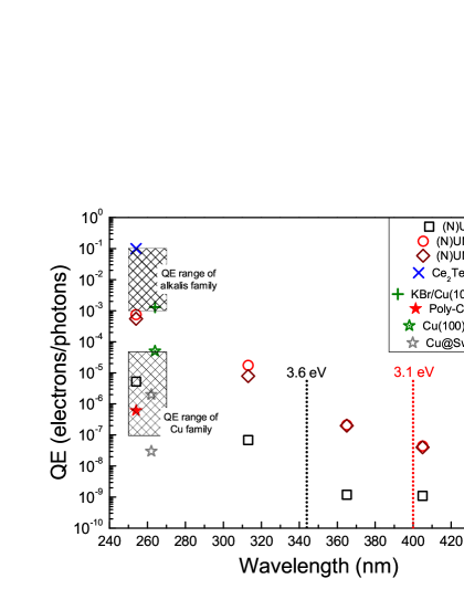
As expected, upon -doping and H-termination, UNCD sensitivity shifted toward near UV/visible wavelengths. There are two main features in Fig.3 we would like to stress. The first feature is QE in the band 250-270 nm which is of common interest to the photocathode community. QE of the originally grown (N)UNCD was 5.310-6. Given the measured WF 3.6 eV, it is a quite moderate effect compared to the single crystal Cu (100) QE of 510-5 with WF=4.2 eV.21 Remarkably, the QE was enhanced by a factor of 140 upon H-termination, setting (N)UNCD at the low boundary of a QE range of alkali-based photocathodes. Secondly, diamond films were sensitive in visible blue. KP results suggest that in all cases photoemission was in the sub-WF regime. For (N)UNCD at 365 and 405 nm and for (N)UNCD:H at 436 nm, this seems a plausible conclusion. It can be explained by emission from grain boundaries with a lowered WF, caused by the local environment,22 accounted also for strong field emission from flat polycrystalline diamond surfaces.23 Photoemission from (N)UNCD:H in visible blue at 405 nm is most probably a regular threshold process – photon energy of 3.06 eV versus WF 3.070.01 eV and 3.150.01 eV as determined by KP (light green and olive solid lines in Fig.2b). In any of the 2 regimes, incorporation of nitrogen lead to sustainable currents from UNCD surfaces in the blue range.
In conclusion, by combining hydrogen passivation of the surface, lowering the work function, and nitrogen introducing electron states in the band gap close to the conduction band minimum, a proof-of-concept was demonstrated that ultrananocrystalline diamond is an emergent robust high efficiency photocathode. This was accomplished by measuring a QE dependence on wavelength of primary photons. (N)UNCD:H films of 150 nm thickness had a QE of 10-3 at 254 nm, and were sensitive in the visible range (between 405 and 436 nm). It is reasonable to expect that QE in near UV and sensitivity in the visible, toward 532 nm, can be further increased. A route to achieve this requires detailed investigation and optimization of: 1) thickness for the best photon absorption; 2) defect engineering in the band gap to find the best trade-off between donors’ activation energy and donors’ concentration effecting simultaneously the density of states and electron lifetime; and 3) defect engineering on the surface to avoid any upward band bending and to achieve work functions compared with -dopant’s activation energies.
We thank Robert Nemanich and Franz Koeck (ASU) for valuable discussions, and Eric Wisniewski and Zikri Yusof (IIT) for technical assistance. Euclid TechLabs acknowledges support from DOE SBIR, grant DE/SC0009572. Samples were synthesized at the CNM ANL, a U.S. DOE, Office of Science, Office of Basic Sciences User Facility under contract DE-AC02-06CH11357. Funding was provided, in part, by NASA EPSCoR grant NNX13AB22A and NASA Space Grant NNX10AM80H.
References
- (1) D.H. Dowell et al., NIM A 622, 685 (2010).
- (2) E.E. Wisniewski et al., NIM A 711, 60 (2013).
- (3) T. Vecchione et al., Appl. Phys. Lett. 99, 034103 (2011).
- (4) J. Maldonado et al., Phys. Rev. STAB 11, 060702 (2008).
- (5) S. Karkare et al., Phys. Rev. Lett. 112, 097601 (2014).
- (6) M.J. Powers et al., Appl. Phys. Lett. 67, 3912 (1995).
- (7) R.J. Nemanich et al., Diam. Relat. Mater. 5, 790 (1996).
- (8) F. Himpsel et al., Phys. Rev. B 20, 624 (1979).
- (9) J. van der Weide et al., Phys. Rev. B 50, 5803 (1994).
- (10) A.S. Tremsin et al., SPIE Proc. 4139, 16 (2000).
- (11) X. Chang et al., Phys. Rev. Lett. 105, 164801 (2010).
- (12) A. Laikhtman et al., Appl. Phys. Lett. 73, 1433 (1998).
- (13) P. Kulkarni et al., J. Appl. Phys. 103, 084905 (2008).
- (14) M. Nesladek, Semicond. Sci. Technol. 20, R19 (2005).
- (15) H.B. Dyer et al., J. Chem. Phys. 42, 1898 (1965).
- (16) J. Cui et al., Phys. Rev. Lett. 81, 429 (1998).
- (17) T. Sun et al., Appl. Phys. Lett. 99, 202101 (2011).
- (18) I.I. Vlasov et al., Phys. Stat. Sol. A 203, 3028 (2006).
- (19) H. Kuzmany et al., Carbon 42, 911 (2004).
- (20) J.S. Kim et al., Synthetic Metals 111-112, 311 (2000).
- (21) W. He et al., Appl. Phys. Lett. 102, 071604 (2013).
- (22) V. Chatterjee et al., Appl. Phys. Lett. 104, 171907 (2014).
- (23) K. Okano et al., Nature 381, 140 (1996).
- (24) F. Le Pimpec et al., J. Vac. Sci. Technol. A 28, 1191 (2010).