Temperature-driven band inversion in Pb0.77Sn0.23Se: Optical and Hall-effect studies
Abstract
Optical and Hall-effect measurements have been performed on single crystals of Pb0.77Sn0.23Se, a IV-VI mixed chalcogenide. The temperature dependent (10–300 K) reflectance was measured over 40–7000 cm-1 (5–870 meV) with an extension to 15,500 cm-1 (1.92 eV) at room temperature. The reflectance was fit to the Drude-Lorentz model using a single Drude component and several Lorentz oscillators. The optical properties at the measured temperatures were estimated via Kramers-Kronig analysis as well as by the Drude-Lorentz fit. The carriers were p-type with the carrier density determined by Hall measurements. A signature of valence intraband transition is found in the low-energy optical spectra. It is found that the valence-conduction band transition energy as well as the free carrier effective mass reach minimum values at 100 K, suggesting temperature-driven band inversion in the material. Density function theory calculation for the electronic band structure also make similar predictions.
pacs:
78.20.-e,78.20.Ci,78.40.FyI Introduction
Class IV-VI narrow-gap compound semiconductors have been of great interest for many decades not only for their scientific interest but also for their use in novel technological instrumentation such as infrared optoelectronics and thermoelectric devices.Nimtz and Schlicht (1983) Crystalizing in the rock salt structure, materials such as PbTe, PbSe, SnTe, and their mixed alloys have been found to have high dielectric constants and quite unusual infrared and electronic properties.Madelung (2004) PbSe and SnSe, the two parent compounds of Pb1-xSnxSe alloy system, have what is commonly known as band inversion.Dimmock et al. (1966) For = 0, , PbSe has the conduction band in L symmetry and the valence band symmetry is denoted by L. As one increases in the alloy system, Pb1-xSnxSe, the band gap initially reduces and then closes, with a linear dispersion around the Fermi level. Subsequent increase in reopens the gap but now the valence band symmetry gets inverted to L, whereas symmetry of the conduction band changes to L, identical to SnSe, , = 1.
Recent theoretical and experimental interest in these alloys has occurred because they have been suggested to represent a new, non-trivial topological phase called a topological crystalline insulatorFu (2011); Hsieh et al. (2012)(TCIs). As in most topological insulators, observations are complicated because the crystals are usually found to be either p-doped or n-doped due to non-stoichiometry so that surface-state features get overshadowed by an overwhelming bulk-carrier contribution. This is the case in the data reported here. Nevertheless, the temperature dependence of the free-carrier effective mass and of the valence-to-conduction band absorption edge could be a suitable point of inquiry to explore the band inversion and temperature-driven phase transition in such materials. So, apart from determining the optical and transport properties, this study also attempts to investigate such a possibility in a Pb0.77Sn0.23Se single crystal.
Studies of PbSe have reported the rock salt crystal structure at ambient temperature and pressure with a lattice parameter of Å and a direct minimum energy band gap of around 0.28 eV at the L point in the Brillouin zone.Delin et al. (1998); Madelung (2004); Harman and Melngailis (1974) In contrast, SnSe has been stabilized as an orthorhombic crystal with layered symmetry and an indirect minimum energy band gap of 0.9 eV.Madelung (2004); Albers et al. (1962) On the basis of X-ray diffraction studies of annealed powders, it has been establishedLittlewood et al. (2010); Dixon and Hoff (1971) that the mixed alloy Pb1-xSnxSe stabilizes in the rock salt structure for and that the minimum band gap remains at the L point. Infrared absorption measurementsStrauss (1967) find that the gap is a complex function of temperature and stoichiometric ratio . An ARPES studyDziawa et al. (2012) of Pb0.77Sn0.23Se finds that the band gap is temperature-dependent, with a minimum around 100 K. The bulk band gap reopens at the L point with an inverted symmetry of the valence band L and the conduction band L as the temperature is further increased.Dziawa et al. (2012)
II EXPERIMENTAL PROCEDURES
Compositional and structural defects play significant role in determination of chemical and electronic properties of lead chalcogens. Local compositional disorder significantly affects the band gap formation for the alloy compositions. In addition, short-range disorder breaks the degeneracy near the band edgeGao and Daw (2008) because PbSe and SnSe represent two different crystal structures. Therefore, controlled crystal growth is an essential requirement.
A vapor-phase growth technique was employed to prepare single crystals of Pb0.77Sn0.23Se. The crystals had the rock salt structure with lattice parameter Å. To ensure good quality samples, quality-control conditions were used, including super-saturation of gaseous phase and a seed crystal with the proper structure and orientation. Lead chalcogen crystals are opaque and have a metallic luster. They are brittle and easily cleave along the (100) plane. Chemical binding in these systems has both ionic and covalent components. A single crystal of size mm3 with smooth (100) crystal plane as the exposed surface was selected for optical measurements.
Temperature dependent (10–300 K) reflectance measurement were conducted using a Bruker 113v Fourier-transform interferometer. A helium-cooled silicon bolometer detector was used in the 40–650 cm-1 spectral range and a DTGS detector was used from 600–7000 cm-1. Room temperature measurement up to 15,500 cm-1 used a Zeiss microscope photometer. Because the rock salt structure of the material implies isotropic optical properties, all optical measurements were performed using non-polarized light at near-normal incidence on the (100) crystal plane. To achieve higher accuracy during reflectance measurements, a small evaporation device incorporated in the metal shroud of the cryostat was used to coat the crystal surface with gold, minimizing changes of experimental conditions during sample and reference single-beam spectral measurements. The gold coating was easy to remove since the material is easily cleaved along the (100) plane.
Optical measurements were followed by Hall-effect measurements, using a physical properties measurement system (PPMS) from Quantum Design which allows transport measurement over 10–300 K. Magnetic fields up to 7 T were applied perpendicular to the (100) plane and ramped in the upward and downward directions while the Hall voltage was measured transverse to current and field. The Hall-effect measurements gave the sign (p-type) and value for the carrier density at 10 K and at room temperature. Errors in the carrier density estimate originate from the non-uniform thickness of the sample, non-rectangular cross section, and contact size. The errors are of course the same at each temperature. These errors do affect the discussion in a later section, where we compare Hall measurements and the infrared plasma frequency , where is the electronic charge and is the effective mass of the holes, Our goal in this comparison is to obtain an estimate of the effective mass. In our analysis, the carrier concentration has been linearly extrapolated over intermediate temperatures for the estimation of effective number of carriers at various temperatures of interest. The volume expansion of the crystal with temperature is also included in this calculation, although it is not very significant. Because of the similarity in the crystal structure and lattice parameter, the linear thermal expansion coefficient for this material is taken to be the same as PbSe.Novikova and Abrikosov (1964)
III EXPERIMENTAL RESULTS
III.1 Hall-effect studies
Previous Hall studiesMartinez (1973); Maier and Daniel (1977) on PbSe and SnSe reported p-type carriers in these materials. A slight increase in p-type carrier density at room temperature compared with 70 K was observed in SnSe.Julien et al. (1992) The origin of the p-type extrinsic carrier in the crystal is due primarily to the presence of ionized lattice defects associated with deviations from stoichiometry, possibly due to excess of selenium or vacancies occupied by acceptor impurities.Strauss and Brebrick (1968); Asanabe (1959); Goldberg and Mitchell (1954) Our Hall measurements show p-type carriers with a concentration of cm-3 at room temperature. This value increases to cm-3 at 10 K. The relatively high value for suggests that our sample is a degenerate semiconductor, in which the chemical potential is pushed down into the valence band due to the carrier density exceeding the valence band edge density of states.
III.2 Reflectance spectra
The temperature dependence of the reflectance of Pb0.77Sn0.23Se between 40 and 7000 cm-1 (5 meV–870 meV) is shown in Fig. 1. In the far-infrared range, a high reflectance is observed, decreasing somewhat as temperature increases. The effect of an optically-active transverse phonon may be seen around 40–200 cm-1. This feature weakens as temperature increases.Habinshuti et al. (2013) A rather wide valence intraband transition centered around 650 cm-1 and shifting to lower frequency with increasing temperature affects the reflectance; this is evident at low temperatures causing a rise in the reflectance level around the central frequency.Wehrenberg et al. (2002) There is a plasma minimum around 930 cm-1 at 10 K; this feature shifts to around 885 cm-1 as temperature increases to 300 K and becomes slightly less deep. As we shall see, it is in good agreement with the zero crossing of the Kramers-Kronig derived real part of the dielectric function .
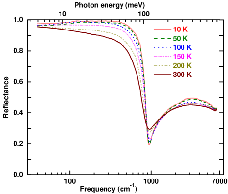
In the midinfrared, we observe interband transitions from the occupied states in the valence band to the conduction band. These transitions become weaker, leading to decreased reflectance, as the temperature is increased. As this is a p-type system, the chemical potential lies in the valence band; therefore, the experimentally-observed minimum absorption edge in the midinfrared range is an overestimate of the direct band gap at the L point of the Brillouin zone, as would be observed in an intrinsic Pb0.77Sn0.23Se crystal.
The top panel of Fig. 2 shows the 300 K reflectance up to 1.92 eV. There is a strong high-energy interband transition at 10,600 cm-1 (1.3 eV).
IV ANALYSIS
IV.1 Kramers-Kronig analysis and optical conductivity
We used the Kramers-Kronig relations to analyze the bulk reflectance and then to estimate the real and imaginary parts of the dielectric function.Wooten (1972) Before calculating the Kramers-Kronig integral, the low frequency reflectance data were extrapolated to zero using the reflectance-fit parameters. (The fit is discussed later in this section.) Reflectance data above the highest measured frequency were extrapolated between 80,000 and cm-1 with the help of X-ray-optics scattering functions; from the scattering function for every atomic constituent in the chemical formula and the volume/molecule (or the density) one may calculate the optical properties in the X-ray region.Henke et al. (1993) A power-law in was used to bridge the gap between the data and the X-ray extrapolation. Finally, an power law was used above cm-1. The optical properties were derived from the measured reflectance and the Kramers-Kronig-derived phase shift on reflection.
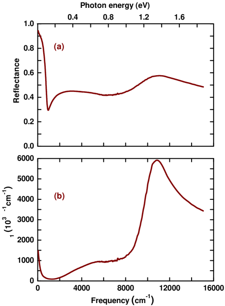
The lower panel of Fig. 2 shows the Kramers-Kronig-derived optical conductivity at 300 K. The narrow Drude contribution and the contributions to the conductivity from interband transitions around 3500, 5100, and 10,600 cm-1 are consistent with the reflectance.
The temperature dependence of the Kramers-Kronig derived real part of the optical conductivity, over 40–7000 cm-1 is shown in Fig. 3. The far-infrared range shows the Drude contribution to . Between 10–100 K, the Drude relaxation rate is below the measured frequency range, explaining the non-constant area under the displayed conductivity spectrum as temperature changes. The relaxation rate increases as temperature is increased until, by 200 K, most of the Drude spectral weight is seen in the figure.
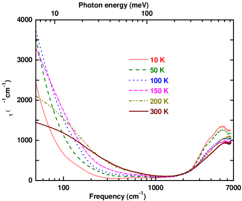
The Drude conductivity partially overlaps with a small and dispersive contribution from the valence intraband transition at 650 cm-1. This feature can be seen in the spectra at 10–100 K but becomes masked by the Drude spectrum as temperature increases. The valence intraband transition is an excitation from an occupied state below the Fermi level to an empty state (in another valence subband) above the Fermi level. It would only be observed if the Fermi level were to lie somewhere within the valence band.
In the midinfrared range, the optical conductivity decreases as temperature is increased. At most temperatures, two overlapping conductivity peaks may be discerned around 3500 and 5100 cm-1; these features, arising from interband transition, are also consistent with the reflectance. The onset of the interband transitions is estimated by extrapolating linearly the conductivity to . This intercept is about 2300 cm-1 at 10 K, then decreases to around 2200 cm-1 at 100 K, and then increases back to 2300 cm-1 at 300 K. The temperature dependence of all parameters is discussed in a following subsection.
IV.2 The real part of the dielectric function
The Kramers-Kronig result also allows us to estimate the real part of dielectric function shown in Fig. 4. At low frequencies, is negative, a defining property of a metal. The temperature dependence of the free-carrier scattering rate is very evident in this dielectric function plot. For temperatures above 150 K, becomes almost flat at low frequencies, implying that the scattering rate is on the order of a few hundred cm-1. In contrast, at low temperatures , sharply decreasing, indicating a very small scattering rate, one below the minimum measured frequency.
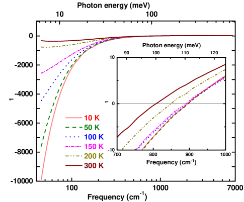
The inset graph shows the zero crossing of (representing the screened plasma frequency) for different temperatures. At 10 K the screened plasma frequency is around 900 cm-1; this value is maintained to about 150 K, after which it decreases to around 815 cm-1 by 300 K. This Kramers-Kronig-derived screened plasma frequency is in good agreement with the reflectance plasma minimum.
IV.3 Sum rule analysis and
Once we have the real part of the conductivity, we can calculate the partial sum using
| (1) |
to obtain the effective number of carriers participating in optical transitions up to frequency . The quantities in this equation are , the effective mass, , the free-electron mass, , the electronic charge, and , the volume taken up by one “molecule” of Pb0.77Sn0.23Se.
Figure 5 shows the temperature-dependent partial sum rule results. The free-carrier contribution saturates around 0.015 at 10 K, decreasing to 0.011 at 300 K. These data suggest that either the carrier density is decreasing or the effective mass is increasing as temperature increases. The Hall results tell us that it is the former. We use the Hall carrier density to estimate the free carrier effective mass and its temperature dependence. The results are shown in Fig. 6. A uniform error is added to the data points based on the uncertainty in the and the optical conductivity-dependent partial sum rule derived from Karamers-Kronig relations.
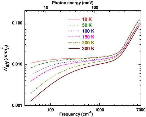
The effective mass changes only slightly over the range of measurements; there is a weak minimum at 100 K where and then a rise to at 300 K. The average effective mass is .
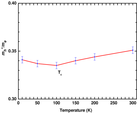
We note that on account of the doping, the Fermi level is far from the putative Dirac point, and, moreover that the optical conductivity spectrum from which this effective mass is derived is an angular average over the Fermi surface and an energy average over a scale set by the relaxation rate, .
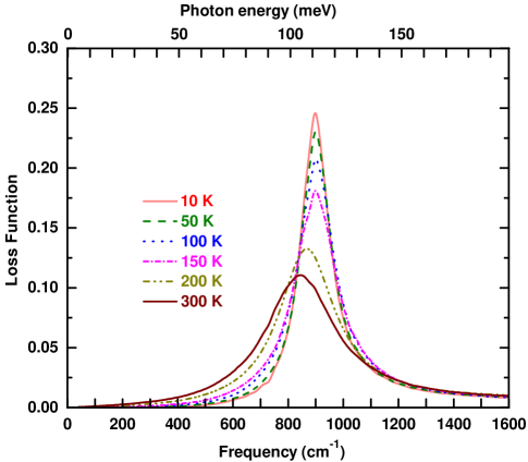
IV.4 Energy-loss function
Finally, the temperature dependence of the longitudinal response of this material, namely the loss function , is plotted against frequency in Fig. 7. The free-carrier peak in the loss function is a good estimate of the screened Drude plasma frequency. This estimate is in good agreement with the zero crossing of in Fig. 4 as well as the value calculated by fitting with the Drude-Lorentz model, discussed in the next section.
IV.5 Drude-Lorentz model fits
We used the Drude-Lorentz model to fit the reflectance data. The Drude component characterizes the free carriers and their dynamics at zero frequency whereas the Lorentz contributions are used for the optically-active phonon in the far-infrared region along with valence intraband and interband transitions in the mid and near infrared. The dielectric function is:
| (2) |
where the first term represents the core electron contribution (transitions above the measured range, the second term is free carrier contribution characterized by Drude plasma frequency and free carrier relaxation time and the third term is the sum of six Lorentzian oscillators representing phonons, valence intraband, and interband electronic contributions. The Lorentzian parameters are the th oscillator plasma frequency , its central frequency , and its linewidth . This dielectric function model is used in a least-squares fit to the reflectance.
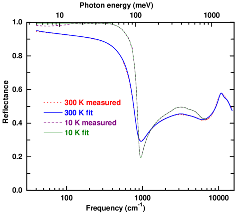
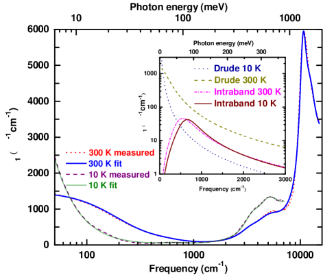
Figure 8 compares the calculated and measured reflectance at 10 K and 300 K; the 300 K fit is shown up to 15,500 cm-1 whereas the 10 K data are fitted to 7000 cm-1. Similar quality fits were obtained at all other temperatures.
The comparison between the Kramers-Kronig-derived and the Drude-Lorentz-model conductivity spectra at 10 K and 300 K is shown in Fig. 9. The parameters are the ones used to fit the reflectance. That the agreement is good gives us confidence in both procedures. The inset graph shows the Drude contribution and the valence intraband contributions at 10 K and 300 K. The valence intraband peak is small and dispersive but is necessary for a good description of the data. Table I lists the 21 parameters used during the fitting routine to fit the reflectance and the conductivity spectra at 300 K.
| Modes assignment | Oscillator | Central | Linewidth |
| in fitting | strength | frequency | |
| routine | (cm-1) | (cm-1) | (cm-1) |
| Drude | 4160 | 0 | 195 |
| Optical phonon | 240 | 40 | 5.5 |
| Valence intraband | 1230 | 550 | 560 |
| Interband 1 | 4550 | 3500 | 1900 |
| Interband 2 | 11,000 | 5120 | 3950 |
| Interband 3 | 20,630 | 10,620 | 1950 |
| Interband 4 | 23,750 | 12,350 | 4150 |
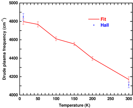
Figures 10–13 show the temperature dependence of selected parameters from the fits. First, Fig. 10 shows the Drude plasma frequency, whose strength decreases as temperature increases. We also show a plasma frequency calculated from the Hall measurement where comes from the Hall data and from the sum rule analysis for the free carriers. Within the error bars, the two results agree.
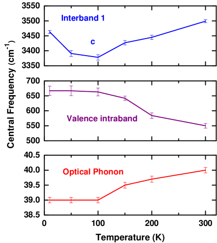
Secondly, the temperature dependence of the central frequencies of the lowest interband transition, the valence intraband transition and the optical phonon is shown in Fig. 11. The lowest interband transition has its minimum value at K. As temperature increases, the valence intraband oscillator shifts towards lower frequencies whereas the phonon mode in the far-infrared range shifts slightly towards higher frequencies.
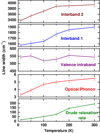
The linewidth of many of these modes suggests significant overlap amongst them, especially in the midinfrared region. Figure 12 shows the temperature dependence of the linewidth of these transitions. The Drude relaxation rate (bottom panel) becomes as small as 17 cm-1 (well below our experimental low frequency limit) at 10 K, increasing with temperature to 195 cm-1 at 300 K. The corresponding hole mobility decreases from 1630 cm2/Vs at 10 K to 140 cm2/Vs at 300 K. Based on these hole mobility values, the optical conductivity is estimated to be 23,200 -1cm-1 at 10 K, decreasing to 1320 -1cm-1 at 300 K. These estimates are in good agreement with the conductivity values found from the fitting routine: 21,800 -1cm-1 at 10 K, decreasing to 1490 -1cm-1 at 300 K. The linewidth of every other oscillator shows a similar temperature trend except for the valence intraband mode which has a weak (and not very significant) minimum at 100 K.
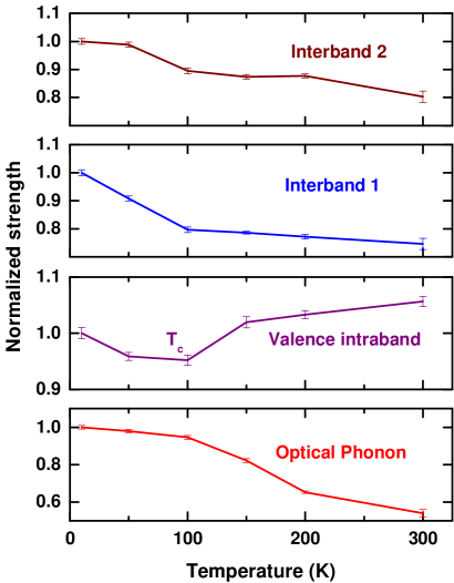
Finally, the temperature dependence of the oscillator strength for several oscillators is shown in Fig. 13. The strength has been normalized by its value at 10 K. (The Drude oscillator strength is shown in Fig. 10.) Three oscillators have their highest strength at the lowest temperature; it decreases monotonically as temperature increases, with a change of slope around 100 K. The valence intraband mode is different: its shows a clear minimum at 100 K and is higher at 300 K than at 10 K.
V DISCUSSION
V.1 Free carrier characteristics and band inversion
A scattering rate calculation for a p-type Si1-xGex alloy predicts quite a high scattering rate.Joyce et al. (2007) Impurity scattering is expected to be strong on account of the disorder associated with the alloy. In contrast, our Pb0.77Sn0.23Se single crystal has a quite small free carrier scattering rate at low temperature. Indeed, the free-carrier scattering rate (shown in the bottom panel of Fig. 12) remains temperature dependent below 50 K. Considering the alloy form of the material with large stoichiometric imbalance, this result is rather surprising.
Previous studies have shown that the extrinsic carrier density in Pb1-xSnxSe affects not only the Hall coefficient but also its temperature dependence. For lightly doped systems, changes sign from positive to negative as temperature is increased, mainly due to the increasing type contribution from thermally excited carriers. On the other hand, for heavily doped systems, the Hall coefficient is positive throughout and has weak temperature dependence.Dixon and Hoff (1971) As temperature is increased, due to increasing thermal energy, the number of free carriers increases. However an increase in the band gap due to increasing temperature also reduces the number of thermally excited carriers. The value of the Hall coefficient depends on the relative dynamics of these two opposing mechanisms. The slight increase in the Hall coefficient with temperature in our sample could be due to an imbalance between these two competing processes.
Temperature dependent ARPES measurements of the (100) surface of Pb0.77Sn0.23Se monocrystals have been interpreted as finding band inversion in the material around 100 K.Dziawa et al. (2012) The band curvature at the L point changes during band inversion and band dispersion becomes almost linear during gap closure at 100 K. The temperature dependence of the carrier effective mass (shown in Fig. 6) does show a weak minimum, in agreement with this idea.
V.2 Minimum band gap and the valence intraband transition
The phenomenon of first shrinking and then expansion of band gap as temperature is decreased should affect the minimum absorption edge directly. Fig. 11 shows that the central frequency of the lowest interband transition has a minimum at 100 K. In addition, the onset of this interband transition, estimated by linear extrapolation of the low-energy edge in the Kramers-Kronig-derived optical conductivity to zero conductivity suggests a similar trend. An ARPES study also finds a minimum band gap at 100 K.Dziawa et al. (2012)
We can point to other features in the optical spectrum that present themselves around 100 K: the frequency of the optically-active phonon (Fig. 11) and the linewidth and the spectral weight of the valence intraband transition (Figs. 12 and 13).
V.3 Electronic structure calculations
The energy band structure of Pb0.75Sn0.25Se was calculated within density-functional theory using the VASP package.Kresse and Hafner (1993, 1994); Kresse and Furthmüller (1996a, b) The input structure consists of 8 atoms cell with 3 Pb, 1 Sn and 4 Se atoms. The calculation was based on a generalized gradient approximation (GGA) for the exchange-correlation potential using the Perdew, Burke, and Ernzerhof formalismPerdew et al. (1996) along with spin-orbit coupling for both geometric and electronic optimization. We used an energy cutoff of 500 eV, 10-6 eV energy minimization, and -points. The calculation gave a lattice constant of 6.16 Å, an overestimate by 0.09 Å compared with the measured lattice constant.Haas et al. (2009) The electronic band structure was calculated along high-symmetry -points in the Brillouin zone with the Fermi energy fixed to zero (i.e., an undoped crystal). As shown in Fig. 14, the band structure calculation indicates that the material has a direct band gap at the L-point in the Brillouin zone with an energy gap of 0.20 eV. Fig. 15 shows an enlarged view of the conduction band minimum and the valence band maximum at the L point.
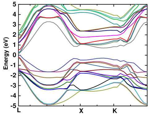
The spin-orbit interaction is important in determining the actual band ordering, band splitting and the details of the electronic structure in class IV-VI narrow-gap semiconductors. Fig. 15 shows the splitting of the valence band into 3 valence sub-bands. The splitted valence bands are named as split-off, heavy-hole and light-hole bands.Pankove (1971); Braunstein and Kane (1962)
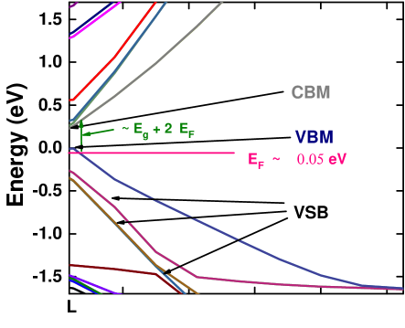
This VASP calculation also produced the density of states. Using the carrier density from experiment and this density of states, we can estimate that the Fermi energy in our doped sample lies around meV. The lowest interband transition takes place from to the empty state in the conduction band at the same -point . The band structure calculation then predicts this absorption to start around 0.30 eV (2420 cm-1). This prediction is in good agreement with the estimate of 2300 cm-1 from the threshold for the interband transitions seen in the optical conductivity.
In addition to the optical interband transitions between the valence and the conduction band, there are also optical transitions within the valence band, the valence intraband transition discussed above. These transitions are seen in a number of p-type semiconductors, when the top of the valence band is populated with holes. It is then possible to make intraband transitions from low-lying sub-bands to states above the Fermi level. These transitions have been observed in a number of semiconductors, including Ge, GaAs, and InSb.Kaiser et al. (1953); Gobeli and Fan (1960); Gru (2006) The single crystal of Pb0.77Sn0.23Se shows similar valence intraband transitions whose temperature dependence is shown in Figs. 11–13.
VI CONCLUSIONS
Hall measurements of Pb0.77Sn0.23Se single crystals disclose the p-type nature of the material and show that the carrier density decreases from cm-3 at 10 K to cm-3 at 300 K. Temperature-dependent optical reflectance measurement shows degenerate semiconductor behavior. At 10 K, the screened Drude plasma minimum lies around 930 cm-1; it shifts slightly towards lower frequency as temperature increases.
In the midinfrared and near-infrared region, the spectra show valence intraband transition and valence to conduction band excitations. The temperature dependence of the lowest-energy interband transition energy shows a minimum at 100 K. This behavior suggest band inversion in the material, also predicted by many other previous studies. The effective hole mass also has a minimum value at 100 K consistent with linear band dispersion at the L point in the Brillouin Zone. Theoretical calculations provide the details of electronic band structure, supporting the existence of valence intraband transition. Our experimental and theoretical studies suggest that material undergoes a temperature-driven band inversion at the L point as also predicted by previous study.Dziawa et al. (2012)
Acknowledgements.
The author wish to thank Xiaoxiang Xi for his constructive discussions on material’s band structure. This work was supported by the DOE through contract No. DE-AC02-98CH10886 at Brookhaven National Lab and by the NSF DMR 1305783 (AFH).References
- Nimtz and Schlicht (1983) G. Nimtz and B. Schlicht, Narrow-Gap Semiconductors, Springer Tracts in Modern Physics, Vol. 98 (Springer Berlin Heidelberg, 1983) pp. 1–117.
- Madelung (2004) O. Madelung, Semiconductors: Data Handbook (Springer Berlin Heidelberg, 2004) pp. 566–605.
- Dimmock et al. (1966) J. O. Dimmock, I. Melngailis, and A. J. Strauss, Phys. Rev. Lett. 16, 1193 (1966).
- Fu (2011) L. Fu, Phys. Rev. Lett. 106, 106802 (2011).
- Hsieh et al. (2012) T. H. Hsieh, H. Lin, J. Liu, W. Duan, A. Bansil, and L. Fu, Nat. Commun. 3, 982 (2012).
- Delin et al. (1998) A. Delin, P. Ravindran, O. Eriksson, and J. M. Wills, Int. J. Quantum Chem. 69, 349 (1998).
- Harman and Melngailis (1974) T. Harman and I. Melngailis, Narrow Gap Semiconductors, Appl. Solid state Sci., Vol. 4 (Elsevier, 1974) pp. 1 – 94.
- Albers et al. (1962) W. Albers, C. Haas, H. Ober, G. Schodder, and J. Wasscher, J. Phys. Chem. Solids 23, 215 (1962).
- Littlewood et al. (2010) P. B. Littlewood, B. Mihaila, R. K. Schulze, D. J. Safarik, J. E. Gubernatis, A. Bostwick, E. Rotenberg, C. P. Opeil, T. Durakiewicz, J. L. Smith, and J. C. Lashley, Phys. Rev. Lett. 105, 086404 (2010).
- Dixon and Hoff (1971) J. R. Dixon and G. F. Hoff, Phys. Rev. B 3, 4299 (1971).
- Strauss (1967) A. J. Strauss, Phys. Rev. 157, 608 (1967).
- Dziawa et al. (2012) P. Dziawa, B. J. Kowalski, K. Dybko, R. Buczko, A. Szczerbakow, M. Szot, E. Å usakowska, T. Balasubramanian, B. M. Wojek, M. H. Berntsen, O. Tjernberg, and T. Story, Nat. Mater. 11, 1023 (2012).
- Gao and Daw (2008) X. Gao and M. S. Daw, Phys. Rev. B 77, 033103 (2008).
- Novikova and Abrikosov (1964) S. I. Novikova and N. K. Abrikosov, Sov. Phys. Solid State 5, 1397 (1964).
- Martinez (1973) G. Martinez, Phys. Rev. B 8, 4686 (1973).
- Maier and Daniel (1977) H. Maier and D. Daniel, J. Electron. Mater. 6, 693 (1977).
- Julien et al. (1992) C. Julien, M. Eddrief, I. Samaras, and M. Balkanski, Mater. Sci. Eng., B 15, 70 (1992).
- Strauss and Brebrick (1968) A. J. Strauss and R. F. Brebrick, J. Phys. Colloques 29, C4 (1968).
- Asanabe (1959) S. Asanabe, J. Phys. Soc. Jpn. 14, 281 (1959).
- Goldberg and Mitchell (1954) A. E. Goldberg and G. R. Mitchell, J. Chem. Phys. 22, 220 (1954).
- Habinshuti et al. (2013) J. Habinshuti, O. Kilian, O. Cristini-Robbe, A. Sashchiuk, A. Addad, S. Turrell, E. Lifshitz, B. Grandidier, and L. Wirtz, Phys. Rev. B 88, 115313 (2013).
- Wehrenberg et al. (2002) B. L. Wehrenberg, C. Wang, and P. Guyot-Sionnest, J. Phys. Chem. B 106, 10634 (2002).
- Wooten (1972) F. Wooten, Optical Properties of Solids (Academic Press, New York, 1972).
- Henke et al. (1993) B. Henke, E. Gullikson, and J. Davis, At. Data Nucl. Data Tables 54, 181 (1993).
- Joyce et al. (2007) S. Joyce, F. Murphy-Armando, and S. Fahy, Phys. Rev. B 75, 155201 (2007).
- Kresse and Hafner (1993) G. Kresse and J. Hafner, Phys. Rev. B 47, 558 (1993).
- Kresse and Hafner (1994) G. Kresse and J. Hafner, Phys. Rev. B 49, 14251 (1994).
- Kresse and Furthmüller (1996a) G. Kresse and J. Furthmüller, Comput. Mater. Sci. 6, 15 (1996a).
- Kresse and Furthmüller (1996b) G. Kresse and J. Furthmüller, Phys. Rev. B 54, 11169 (1996b).
- Perdew et al. (1996) J. P. Perdew, K. Burke, and M. Ernzerhof, Phys. Rev. Lett. 77, 3865 (1996).
- Haas et al. (2009) P. Haas, F. Tran, and P. Blaha, Phys. Rev. B 79, 085104 (2009).
- Pankove (1971) J. Pankove, Optical Processes in Semiconductors (Dover, 1971).
- Braunstein and Kane (1962) R. Braunstein and E. Kane, J. Phys. Chem. Solids 23, 1423 (1962).
- Kaiser et al. (1953) W. Kaiser, R. J. Collins, and H. Y. Fan, Phys. Rev. 91, 1380 (1953).
- Gobeli and Fan (1960) G. W. Gobeli and H. Y. Fan, Phys. Rev. 119, 613 (1960).
- Gru (2006) The Physics of Semiconductors (Springer Berlin Heidelberg, 2006) pp. 213–249.