Topological states of non-Dirac electrons on triangular lattice
Abstract
We demonstrate the possibility of topological states for non-Dirac electrons. Specifically it is shown that, because of the crystal symmetry and time reversal symmetry, and orbits accommodated on triangular lattice exhibit a quadratic band touching at point at the Fermi level. When the atomic spin-orbit coupling (SOC) is taken into account, a gap is opened resulting in a quantum spin Hall effect state. As revealed explicitly by a model, the topology is associated with a meron structure in the pseudo spin texture with vorticity two, a mechanism different from honeycomb lattice and the band inversion. One possible realization of this scheme is the 1/3 coverage by Bi atom adapted on the Si[111] surface. First-principle calculations are carried out, and a global gap of eV is observed. With the Si substrate taking part in realizing the nontrivial topology, the present template is expected to make the integration of topological states into existing electronics and photonics technologies promising.
pacs:
73.20.-r, 73.43.-f, 73.22.-f, 71.70.EjIntroduction — Topology in condensed matters has been attracting significant interest in recent years Klitzing et al. (1980); Nayak et al. (2008); Kitaev and Laumann ; Hasan and Kane (2010); Qi and Zhang (2011). Because of the bulk-edge correspondence, topological systems exhibit robust surface states. The surface current of a topological insulator is dissipationless, which may resolve the issue of Joule heating in nanoscale electronics, and the Majorana quasi-particle excitations of topological superconductor may be exploited for decoherence-free quantum computation.
By now topological states without strong external magnetic field have been proposed theoretically and some are realized experimentally in various systems Haldane (1988); Kane and Mele (2005a, b); Bernevig et al. (2006); König et al. (2007); Zhang et al. (2009a); Roushan et al. (2009); Zhang et al. (2009b); Xia et al. (2009); Alpichshev et al. (2010); Hasan and Kane (2010); Qi and Zhang (2011); Knez et al. (2011); Beidenkopf et al. (2011). The topology of electronic bands is characterized by non-zero Chern number for time-reversal symmetry broken systemsThouless et al. (1982), and spin Chern number (elaborated as index) in time reversal symmetric systemsKane and Mele (2005a, b); Fu et al. (2007). It is illuminating to understand Chern numbers in various systems in terms of topological texture of pseudo spin in momentum space. On honeycomb lattice, the pseudo spin referring to the two sublattices exhibits two merons at the Dirac cones at and points, each contributing a topological charge 1/2. As seen in the Haldane model and Kane-Mele model Haldane (1988); Kane and Mele (2005a, b), topological states such as quantum anomalous Hall effect (QAHE) and quantum spin Hall effect (QSHE) can be achieved by tuning the signs of mass terms at and points Liang et al. (2013). Bernevig, Hughes and Zhang revealed that in the HgTe/CdTe quantum well a band inversion takes place at point and generates a QSHE state, where the Dirac property sets in due to the opposite parities of the two relevant electronic bands(Bernevig et al., 2006). In this case, the pseudo spin referring to the two orbits develops a skyrmion in momentum space with topological charge of unity. In both schemes, the interactions between two pseudo spin states are linear with momentum. Partially because of this historical reason, topological states are sometimes understood as a unique property of Dirac electrons.
In the present work, we address the topology of non-Dirac electrons taking into account the effect of crystal symmetry and spin-orbit coupling (SOC). It is revealed that, featured by quadratic, non-Dirac dispersions, the relevant pseudo spin texture is a single meron with vorticity two carrying a topological charge of unity. As a specific case, we consider the Si[111] surface with 1/3 coverage by Bi atoms. In this system, Bi atoms are adapted regularly on the top layer of Si atoms and form a triangle lattice with large unit cell of , characterized by the symmetry. The orbits of Bi atoms and those of Si atoms beneath them form a strong bonding state, and become inactive. The and orbits of Bi atoms and the orbits of the other two uncovered Si atoms remain active. At point, the and orbits are close to the Fermi level, which with SOC contribute to form a QSHE insulating state in a unique way featured by the crystal symmetry as well as time reversal symmetry. As a second example, regularly adapted Bi, Au and H atoms on the SiC[111] surface are investigated. While the crystal symmetry is lowered to , similar physics is available as supported by time reversal symmetry.
It is intriguing to notice that topological gaps in the present systems are large, since the strong atomic SOCXu et al. (2013); Zhou et al. ; Song et al. ; Zhang et al. of Bi atoms contributes totally in gap opening. The Si substrate is crucial in providing the crystal symmetry and selecting the orbits of adapted Bi atoms desired for topological states. Therefore, the present template makes it very promising to integrate topological states into existing electronics and photonics devices.
Model Hamiltonian — Let us begin with a model at point for a system characterized by crystal symmetry in additional to time reversal symmetry, with the Bi atoms on triangle lattice in mind. The four-band model around point up to the second order of momentum has the following form
| (1) |
on basis { , , , }, with and . Time reversal symmetry requires the matrix element between them to be an even function of momentum. The rotation symmetry further requires the matrix element between and to take the form of in order to conserve the total angular moment along direction. Therefore, the electrons in the present system are of non-Dirac type. As for the diagonal masses, linear terms in momentum are not allowed since they would change the angular momentum of the basis wave-functions; at the second order of momentum, time reversal symmetry does not permit any asymmetric contribution in and in the individual 22 blocks. The dispersion of Hamiltonian Eq. (1) is then given by , which exhibits a degeneracy and quadratic band touching at point when SOC is absent, a property originated from the property that and belong to a two-dimensional (2D) irreducible representation to crystal symmetry along with time reversal symmetry.
A finite SOC removes this degeneracy and opens a gap, which may result in topologically nontrivial states. Since the atomic SOC is diagonal in this basis, one can first analyze the Berry curvature for the spin-up subspaceXiao et al. (2010)
| (2) |
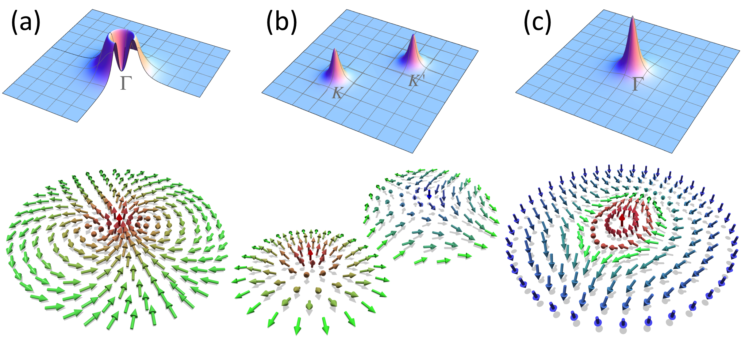
where the Berry connection is defined as and is the occupied state. The dispersion of in momentum space is plotted in Fig. 1(a). The Chern number is evaluated asThouless et al. (1982); Xiao et al. (2010)
| (3) |
This Chern number can be understood from the topological texture of pseudo spin referring to the two orbits in the upper block of Eq. (1) as shown in Fig. 1(a) (a gauge is taken to make real). At point, the pseudo spin is along the north pole; as increases, the pseudo spin vector tilts away and becomes aligned to the equator (namely the plane). Checking the rotation of pseudo spin, we find a rotation around point. This meron texture with vorticity two contributes the unity Chern number in Eq. (3). With time reversal symmetry, one can see the same physics in the spin-down channel. The topology of the whole system is therefore described by the indexKane and Mele (2005b); Fu et al. (2007), which is defined by the spin Chern numbers as Because the particle-hole symmetry is broken by the quadratic term in Eq. (1), the present system falls into the class AIIKitaev ; Ryu et al. (2010).
It is noticed that SOC contributes totally in opening the topological gap in the present scheme, since (and thus index) is always one for nonzero SOC as seen in Eq. (3). This is similar to the case of honeycomb lattice in the Haldane model and Kane-Mele model (Haldane, 1988; Kane and Mele, 2005a), where tuning the signs of mass terms at K and K′ adequately aligns the pseudo spin texture in the two merons (see Fig. 1(b)), and results in various topological states with nonzero integer topological charge in the whole Brillouin zone (BZ) Liang et al. (2013). In contrary, the band inversion in BHZ model (Bernevig et al., 2006) is associated with a skyrmion of the pseudo spin texture (see Fig. 1(c)), where the topological gap is determined by the hybridization of two inverted bands.
Bi on Si[111] surface — To be specific, we investigate the Si[111] surface with 1/3 coverage by Bi atoms. Based on symmetry analysis and first-principles calculations, we show that this system realizes the physics described by the model Hamiltonian Eq. (1).
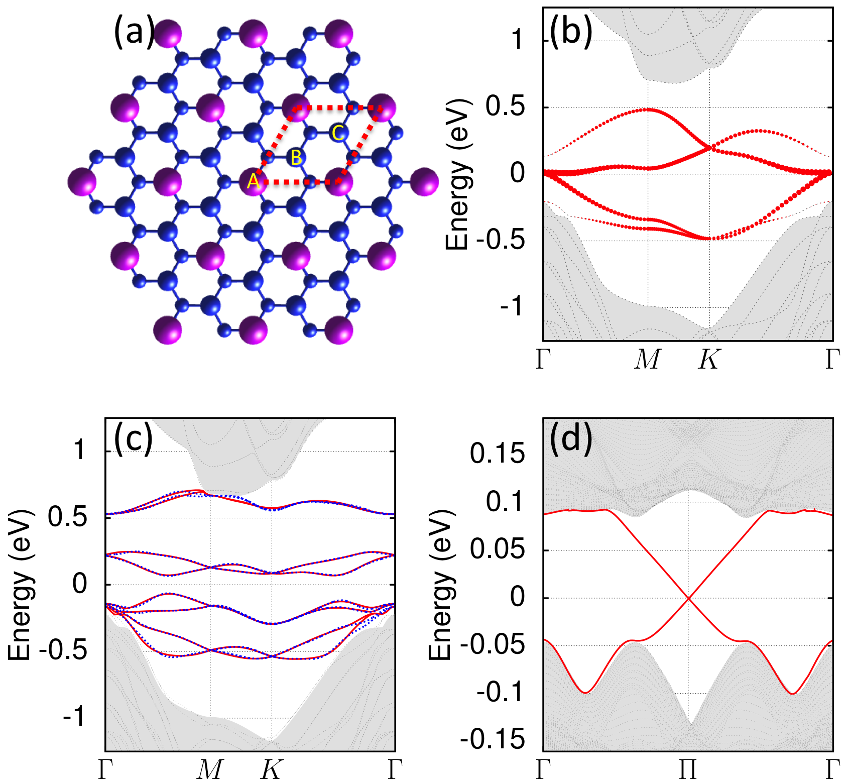
The structure is schematically shown in Fig. 2(a). On the Si[111] surface, the top-most layer Si atoms form a triangle lattice and the unsaturated dangling bonds of Si provide active adsorption sites for various metal atoms. When a unit cell is considered, three sites (A, B and C) of Si surface can be saturated by ad-atoms, which we call A-B-C/Si[111]. A, B and C can either be occupied by atoms such as Bi, Pb, Au, Ag and H, or left vacant where the dangling bonds of Si atoms are unsaturated. Here we consider explicitly the case that A sites are occupied by Bi atoms while B and C sites remain vacant, as shown in the top view in Fig. 2(a). Bi atoms form a triangle sub-lattice and the symmetry group is when the Si substrate is taken into account.
First we study the electronic band structures of this system by first-principles calculations. The calculations were done with the Vienna ab initio simulation package (VASP)Kresse and Furthmüller (1996), where projected augmented-wave (PAW) potential is adoptedBlöchl (1994); Kresse and Joubert (1999). We use the functional introduced by Perdew, Burke, and Ernzerhof (PBE) Perdew et al. (1996) and the generalized gradient approximation (GGA). A 661 mesh in the irreducible Brillouin Zone was used for structure relaxation and 881 mesh for self-consisted calculations. In all the calculations the energy cutoff is set as 500 eV. The forces are relaxed lower than 0.01 eV/. After relaxation, the bond length between the surface Si and the attached Bi becomes 2.58, close to the summation of their ion radius, indicating a strong binding interaction between two atoms. The Bi-Bi distance is 3.84, which is also consistent with the structure of Si[111] surface. The unsaturated Si atoms, on the other hand, form a honeycomb lattice with a Bi atom sitting at the center of each hexagon. All the calculations are done in a slab structure with 12 layers of Si atoms, and a vacuum layer of 10 is included. In order to avoid annoying physics, Si atoms on the bottom surface are saturated by H atoms.
The band structure without SOC is shown in Fig. 2(b). The shadowed (gray color) areas are bulk bands of Si, where the indirect gap of Si crystal is clearly seen. Inside the gap four bands are found from Bi atoms and unsaturated surface Si atoms. The magnitude of the projection of each Bloch states onto the Bi and orbits is represented by the width of red curves. A quadratical touching is found between the second and third bands at point. The Fermi energy passes through this degenerate point and makes the system a zero gap semiconductor. A gap is opened when SOC is turned on as shown in Fig. 2(c). The degeneracy at point originally of four-fold due to the orbital and spin degrees of freedom is lifted partially down to two-fold. Away from the high symmetry point the Rashba SOC due to the broken inversion symmetry at surface lifts the degeneracy totally, which also shifts the position of minimal gap to a midpoint in between and points.
In order to understand the possible topological property of the system, we construct the effective model Hamiltonian around point
| (4) |
on the basis of four orbits , , , inside the gap of bulk Si system, taking into account crystal symmetry and time reversal symmetry. The parameters are evaluated by fitting the results of first-principles calculations as eV, eV, eV, eV and eV.
Around point, the fat-band structure in Fig. 2(b) shows that the two states close to Fermi energy are mainly from Bi orbits and the other two states far away from Fermi energy are contributed mainly by the two orbits of the unsaturated Si atoms. We therefor can down-fold this 44 Hamiltonian into the subspace spanned by orbits. Taking the spin degree of freedom and SOC into consideration, we obtain the 44 effective Hamiltonian as shown in Eq. (1). Therefore, the system is a QSHE insulator as discussed above.
An important character of the QSHE insulating state is the existence of gapless states at the sample edge. We calculate the band structure for a ribbon of width of 50 unit cells based on the maximally localized Wannier function for the surface electronic statesMarzari et al. (2012), where Rashba SOC is included. As shown in Fig. 2(d), there are two gapless edge states connecting the valence and conduction bands for one of the two edges of the ribbon, which cross at the time-reversal invariant point in the 1D BZ. This indicates that this system is in a topologically nontrivial phase with a topological index . It is noticed that the QHSE state survives even in the presence of Rashba SOC, although the global gap is reduced partially.
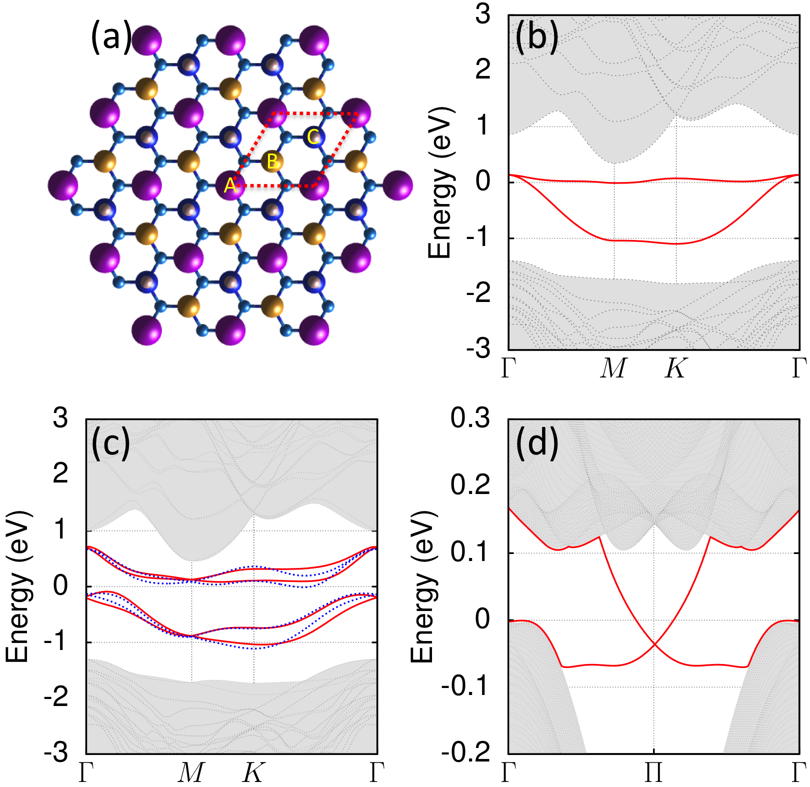
Bi-Au-H on SiC[111] surface — As a second example, we consider the system Bi-Au-H/SiC[111] where a SiC substrate with smaller lattice constant of 3.06 is used as compared with 3.84 for the Si substrate. As can be read from Fig. 3(a), the crystal symmetry is lowered to . Since the orbit of Si atoms is now saturated by Au and H atoms, there are only and orbits in the bulk gap as seen in Fig. 3(b). The degeneracy at point is lifted since the mirror symmetry is absent, while that at point is protected (in absence of SOC) by time reversal symmetry due to the mechanism known for long timeHerring (1937). Therefore, the model Eq. (1) applies to the present system, and a QHSE is realized as evidenced by the gap opening at point upon introducing SOC (Fig. 3(c)) and the gapless edge state in a ribbon structure (Fig. 3(d)).
Discussions and summary— Since orbits (or corresponding orbits) are transformed to each other in the same manner as the orbits under the (and/or ) rotation, QSHE states are also possible with the subbands, supposing other orbits (or orbits) can be filtered in some way Xu et al. (2013); Zhou et al. ; Song et al. .
Let us inspect the possibility of topologically nontrivial states featured by meron with vorticity higher than two. In order to generate a meron with vorticity , the lowest order of momentum in the off-diagonal elements in Eq. (1) should be , which links the two basis wave-functions with the angular-momentum difference . Meanwhile, the basis wave-functions should belong to a 2D irreducible representation of the space groups of crystal, which protects the degeneracy at point in absence of SOC. Let us see the case , with the difference in angular momentum between the basis wave-functions equal to four. In a crystal with (or ) symmetry, the lowest order of momentum in the off-diagonal terms preserving the total angular momentum are , rather than , which generates a meron with vorticity two as discussed above. On the other hand, for a crystal with symmetry, the two wave functions do not form a 2D irreducible representation. Therefore, the meron texture with vorticity two addressed in the present work is unique in generating topological states.
Finally we discuss briefly non-Dirac dispersions in other topological states. In a Chern semimetal HgCr2Se4, the off-diagonal interaction has the form of in the effective Hamiltonian Xu et al. (2011). In their case, there is a quadratic momentum dependence in the diagonal mass terms, which makes the pseudo spin texture not a meron. Quadratically touching band structures at point appear in multi-band systems on honeycomb lattice as discussed in a model system recently, due to the same symmetry Zhang et al. . Because the non-Dirac dispersion is deep in the valence band, it does not contribute directly to the nontrivial topology.
To summarize, we propose the Si[111] surface with Bi atoms adapted as a new template for achieving topological states. With the crystal symmetry and time reversal symmetry, a model is constructed with degeneracy at point and quadratic, non-Dirac type energy dispersion. When the spin-orbit coupling is taken into account, a gap is opened resulting in a quantum spin Hall effect insulator as characterized by a meron pseudo spin texture with vorticity two, in contrast to the widely studied Dirac electrons. In the present scheme, the strong atomic spin-orbit coupling of Bi contributes fully to open the topological gap, and thus provides a new possibility for achieving topological states with large gap which may function even above room temperature. With the Si substrate taking part in realizing the topological state, the present template is expected to make the integration of topological states into existing electronics and photonics devices very promising.
Acknowledgements — The authors are grateful to T. Uchihashi and T. Kawakami for stimulating discussions. This work was supported by WPI Initiative on Materials Nanoarchitectonics, MEXT, Japan, and the Grant-in-Aid for Scientific Research under the Innovative Area “Topological Quantum Phenomen” (No.25103723), MEXT, Japan. Q.F.L acknowledges the support from NSFC under grants 10904092.
Q.F.L. and Y.R. contributed equally to this work.
References
- Klitzing et al. (1980) K. v. Klitzing, G. Dorda, and M. Pepper, Phys. Rev. Lett. 45, 494 (1980).
- Nayak et al. (2008) C. Nayak, S. H. Simon, A. Stern, M. Freedman, and S. Das Sarma, Rev. Mod. Phys. 80, 1083 (2008).
- (3) A. Kitaev and C. Laumann, arXiv: 0904.2771v1 .
- Hasan and Kane (2010) M. Z. Hasan and C. L. Kane, Rev. Mod. Phys. 82, 3045 (2010).
- Qi and Zhang (2011) X.-L. Qi and S.-C. Zhang, Rev. Mod. Phys. 83, 1057 (2011).
- Haldane (1988) F. D. M. Haldane, Phys. Rev. Lett. 61, 2015 (1988).
- Kane and Mele (2005a) C. L. Kane and E. J. Mele, Phys. Rev. Lett. 95, 226801 (2005a).
- Kane and Mele (2005b) C. L. Kane and E. J. Mele, Phys. Rev. Lett. 95, 146802 (2005b).
- Bernevig et al. (2006) B. A. Bernevig, T. L. Hughes, and S.-C. Zhang, Science 314, 1757 (2006).
- König et al. (2007) M. König, S. Wiedmann, C. Brüne, A. Roth, H. Buhmann, L. W. Molenkamp, X.-L. Qi, and S.-C. Zhang, Science 318, 766 (2007).
- Zhang et al. (2009a) H. Zhang, C.-X. Liu, X.-L. Qi, X. Dai, Z. Fang, and S.-C. Zhang, Nature Physics 5, 438 (2009a).
- Roushan et al. (2009) P. Roushan, J. Seo, C. V. Parker, Y. S. Hor, D. Hsieh, D. Qian, A. Richardella, M. Z. Hasan, R. J. Cava, and A. Yazdani, Nature 460, 1106 (2009).
- Zhang et al. (2009b) T. Zhang, P. Cheng, X. Chen, J.-F. Jia, X. Ma, K. He, L. Wang, H. Zhang, X. Dai, Z. Fang, X. Xie, and Q.-K. Xue, Phys. Rev. Lett. 103, 266803 (2009b).
- Xia et al. (2009) Y. Xia, D. Qian, D. Hsieh, L. Wray, A. Pal, H. Lin, A. Bansil, D. Grauer, Y. S. Hor, R. J. Cava, and M. Z. Hasan, Nature Physics 5, 398 (2009).
- Alpichshev et al. (2010) Z. Alpichshev, J. G. Analytis, J.-H. Chu, I. R. Fisher, Y. L. Chen, Z. X. Shen, A. Fang, and A. Kapitulnik, Phys. Rev. Lett. 104, 016401 (2010).
- Knez et al. (2011) I. Knez, R.-R. Du, and G. Sullivan, Phys. Rev. Lett. 107, 136603 (2011).
- Beidenkopf et al. (2011) H. Beidenkopf, P. Roushan, J. Seo, L. Gorman, I. Drozdov, Y. S. Hor, R. J. Cava, and A. Yazdani, Nature Physics 7, 939 (2011).
- Thouless et al. (1982) D. J. Thouless, M. Kohmoto, M. P. Nightingale, and M. den Nijs, Phys. Rev. Lett. 49, 405 (1982).
- Fu et al. (2007) L. Fu, C. L. Kane, and E. J. Mele, Phys. Rev. Lett. 98, 106803 (2007).
- Liang et al. (2013) Q.-F. Liang, L.-H. Wu, and X. Hu, New J. Phys. 15, 063031 (2013).
- Xu et al. (2013) Y. Xu, B. Yan, H.-J. Zhang, J. Wang, G. Xu, P. Tang, W. Duan, and S.-C. Zhang, Phys. Rev. Lett. 111, 136804 (2013).
- (22) M. Zhou, W. Ming, Z. Liu, Z. Wang, Y. Yao, and F. Liu, arXiv: 1401.3392 .
- (23) Z. Song, C.-C. Liu, J. Yang, J. Han, M. Ye, B. Fu, Y. Yang, Q. Niu, J. Lu, and Y. Yao, arXiv: 1402.2399 .
- (24) G.-F. Zhang, Y. Li, and C. Wu, arXiv: 1403.0563 .
- Xiao et al. (2010) D. Xiao, M.-C. Chang, and Q. Niu, Rev. Mod. Phys. 82, 1959 (2010).
- (26) A. Kitaev, arXiv: 0901.2686v2 .
- Ryu et al. (2010) S. Ryu, A. P. Schnyder, A. Furusaki, and A. W. Ludwig, New J. Phys. 12, 065010 (2010).
- Kresse and Furthmüller (1996) G. Kresse and J. Furthmüller, Phys. Rev. B 54, 11169 (1996).
- Blöchl (1994) P. E. Blöchl, Phys. Rev. B 50, 17953 (1994).
- Kresse and Joubert (1999) G. Kresse and D. Joubert, Phys. Rev. B 59, 1758 (1999).
- Perdew et al. (1996) J. P. Perdew, K. Burke, and M. Ernzerhof, Phys. Rev. Lett. 77, 3865 (1996).
- Marzari et al. (2012) N. Marzari, A. A. Mostofi, J. R. Yates, I. Souza, and D. Vanderbilt, Rev. Mod. Phys. 84, 1419 (2012).
- Herring (1937) C. Herring, Phys. Rev. 52, 361 (1937).
- Xu et al. (2011) G. Xu, H. Weng, Z. Wang, X. Dai, and Z. Fang, Phys. Rev. Lett. 107, 186806 (2011).