Nanolithography using counter-propagating light-sheets
Abstract
We propose a laser interference nano-lithography technique for fabrication of nano-structures. This is inspired by a -illumination system that consists of two cylindrical lens arranged face-to-face at a distance with a common geometrical focus. When illuminated by a coherent light, this results in the super-position of two counter-propagating light-sheets. The interference gives rise to nano-bump structures along the optical axis. This technique overcomes the existing point-scanning techniques and paves the way for mass production of nano-structures. Study shows the structures with a feature size of and an inter-nanobump separation of . Proposed technique may find applications in plasmonics, nanophotonics and nanobiology.
Light-sheet microscopy has seen explosive progress in the last decade and it is finding applications in fields ranging from applied physics to nano-biology voie1993 huisken2004 kavya2014 . This techniques was first realized by Siedentopf et al. siedentopf1903 and the first imaging application was demonstrated by Voie et al. voie1993 . Thereafter, the technique was vastly developed by Stelzer group and exploited for potential applications in Biology huisken2004 keller2010 . Many variants of light-sheet microscopy have emerged over the last few years. This include, thin light-sheet microscopy fuchs2002 , ultramicroscopy dodt2007 , digital light-scanning microscopy (DLSM) keller2008 , objective coupled plane illumination microscopy (OCPI) holekamp2008 and confocal light-sheet microscopy silv2012 baum2012 . Over the years, light-sheet based techniques have aided many biological studies dodt2007 ahrens2013 truong2011 fra2011 raju2013 . There are many advantage of light-sheet microscopy over point-scanning techniques and holds a lot of benefit as far as imaging and nano-lithography are concerned. What make light-sheet illumination so special is the large field-of-view and the ability to scan the entire plane in a single-shot. This is very different from the existing point-illumination techniques that require sequential scanning. Light-sheet illumination has the ability of patterning selective plane over a large area with better accuracy and high reproducibility.
Nano-lithography techniques can be broadly divided into two major types i.e, masked and maskless. Fabricated masks and moulds are used to transfer pattern over a desired template for masked lithography technique, while maskless lithography employ some kind of beam (ion beam, electron beam or light beam). Masked lithography has the advantage of high-throughput fabrication over a large area, while maskless techniques use spot size of the beam for precise patterning. Popular masked nano-lithography technique include, nano-imprint lithography chou1996 cattoni2010 , photolithography wagner2010 sanders2010 and soft-lithography xia1998 cooper2011 . On the other hand, maskless lithography include, focused ion-beam lithography mel1987 tseng2004 , electron beam lithography alt2010 gri2009 , scanning probe lithography piner1999 shim2011 and two-photon direct laser writing wollhofen2013 burmeister2012 dong2008 denk1990 . It is the slow serial nature of maskless technique that makes it inappropriate for mass production. So, there is a trade-off between high-throughput production and high precision reproducibility. Ultimately, existing techniques are limited by Abbe’s diffraction limit and thus cannot generate feature smaller than this limit abbe1884 hell2007 . Recently, it has been shown that, diffraction-unlimited nano-lithography can be achieved by using STED technique ben2012 wollhofen2013 . Of-late, high-throughput nano-fabrication using visible light is in demand due to the advancement in nano-technology for enabling mass production of nano-devices.
In this letter, we propose a light-sheet based illumination technique for nano-lithography. The optical configuration consists of two cylindrical lens placed opposite to each other and bear a common geometrical focus. We termed this technique as -system since the aperture angle of combined cylindrical lens system can occupy a maximum angle of . The motivation behind the proposed geometry is to generate multiple nano-bump pattern. Studies show that the nano-bump pattern has an inter-bump separation of approximately . Comparatively, recent developments in laser inference lithography demonstrate an inter-period spacing of , being the inclination angle seo2013 wang2013 . Proposed technique is a simple and efficient way of generating nano-pattens with high reproducibility. Since, this technique produce periodic pattern, so it has potential applications in photonic crystals and submicron sieves.
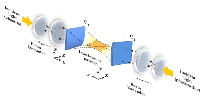
The schematic of the optical configuration for creating periodic nano-bump pattern is shown in Fig.1. The setup consists of two opposing cylindrical lenses and of same focal length (f). The incident coherent beam is allowed to pass through the beam expander to fill the back aperture of the cylindrical lens. When illuminated by the coherent wavefront, both the cylindrical lens give rise to light-sheets which upon superposition generates bump-like interference pattern. The electric field components for a linearly-polarized plane wave at the focus of a cylindrical lens with its axis along x-axis is given by sub2013 ,
| (2) |
is the wavenumber in the image space and is the semi aperture angle. The terms f, and denotes the focal length and refractive index of object and image space respectively. The radial distance from the axis and the polar inclination are denoted by and respectively.
For the cylindrical lens the coordinates with respect to lens are and the resulting field components are,
| (4) |
where,.
The electric field at and near the geometrical focus is the superposition of two counter-propagating electric fields,
| (5) |
So, the field distribution is given by,
| (6) |
where ,
Expansion and simplification produces,
where, .
Similarly, the expressions for and components of the field can be determined by inspection i.e,
| (7) |
and,
| (8) |
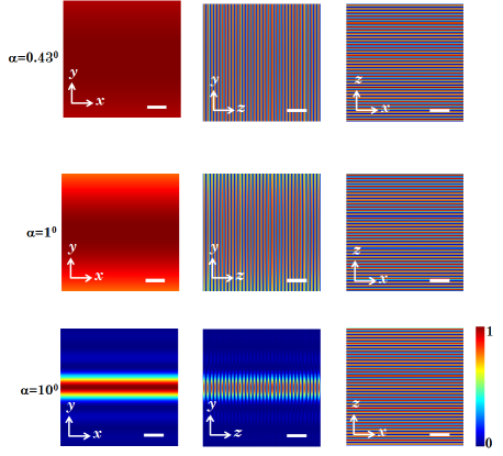
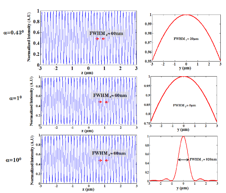
We have carried out computational studies to characterize the field distribution for the proposed light-sheet based -system. Fig.1 shows the schematic diagram of the proposed optical system. The numerical calculations for determining the field distribution at and near the common focus was carried out over a grid size of pixels (along, x,y,z axes). Practically, this spans over a spatial dimension of . An incident light of wavelength is chosen for the study. The field is computed using eqn.(4) for varying semi-aperture angle () of cylindrical lens. Fig.2 shows the field distribution along the optical axis (near focus) for different semi-aperture angles. It is apparent that, the thickness of the sheet scales down with increase in aperture angle from to (see, Fig. 2, XY-profiles). The nano-bump pattern is evident from the - and - planes. Specifically, the field-of-view can be varied along -axis using variable semi-aperture angle. This suggests that such a discrete and dense bump-like pattern can be obtained at nano-scale dimensions. The corresponding intensity plots along axial (z-axis) and lateral (y-axis) axes are shown in Fig.3. From the profile plots it is observed that the z-profile remains unchanged with the change in semi-aperture angle () while the change along y-axis is significant. Specifically, the along y-axis varies from to for to . We observed that, the separation between two successive maxima is () whereas, the full width at half maxima () of the individual nano-bump is approximately .
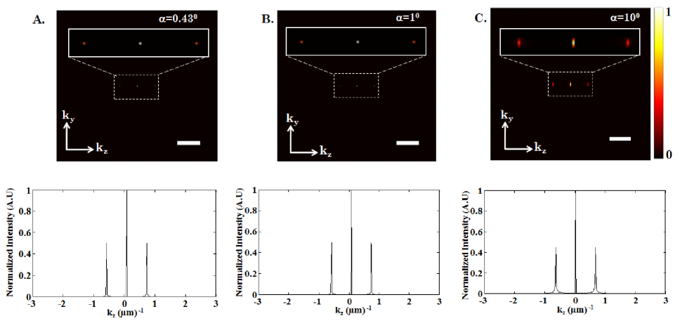
To better understand the nano-pattern characteristics, we obtained the optical transfer function (OTF). This provides the information about the spatial frequencies present in the generated nano-bump pattern. The corresponding -plane is shown in Fig.4 for semi-aperture angles, . One can immediately observe higher spatial frequencies along -axis. OTF shows maximum bandwidth along axial direction but it is not continuous and are separated. Specifically, the low frequency component occur at and a relatively weak higher frequency components can be observed at .
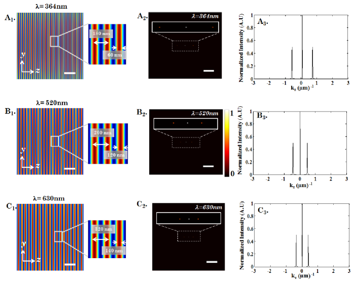
For widespread applicability of the proposed technique, we have also studied the response of the proposed optical system at varying illumination wavelengths. Fig.5 () shows the yz plane of the field distribution for illumination wavelengths, . The inset show a pitch of with the width of each feature (nano-bump) of approximately respectively. Fig. correspond to the OTF at varying wavelengths. The spacing between the low and high freqiency components is quite evident. Moreover, the spacing is found to vary with illumination wavelength. This is clearly reflected in the adjoining intensity plots, Fig.. This facilitates the scaling of distance between nano-bump and specific feature size.
In conclusion, we have proposed an efficient technique for fabricating periodic nano-structures. Unlike point-scanning techniques, we have employed interfering light-sheets configured in a geometry. This has the advantage of high-throughput production when compared to point-scanning techniques. Phase matching is ensured for the counter-propagating light-sheets which upon superposition gives rise to nano-bump structures. The grating pattern thus generated has a feature (bump-width) of , and inter-bump spacing of . This technique will benefit mass production of nano-structures for applications in nano-electronics and nano-biology.
References
- (1) A. H. Voie, D. H. Burns, and F. A. Spelman, J. Microsc. 170, 229 (1993).
- (2) J. Huisken, J. Swoger, F. Del Bene, J. Wittbrodt, and E. H. K. Stelzer, Science 305, 1007 1009 (2004).
- (3) K. Mohan and Partha P. Mondal, Micros. Res. Tech. 77, 105 109 (2014).
- (4) Klaus Greger, Manuel J. Neetz, Emmanuel G. Reynaud, and Ernst H.K. Stelzer, Opt. Exp. 19, 20743 (2011).
- (5) H. Siedentopf and R. Zsigmondy, Annalen der Physik 10, 1 (1903).
- (6) P. J. Keller, A. D. Schmidt, A. Santella, K. Khairy, Z. Bao, J. Wittbrodt, and E. H. Stelzer, Nat. Meth. 7, 637 (2010).
- (7) E. Fuchs, J. S. Jaffe, R. A. Long, and F. Azam, Opt. Exp. 10, 145 (2002).
- (8) H. U. Dodt, U. Leischner, A. Schierloh, N. Jhrling, C. Mauch, K. Deininger, J. M. Deussing, M. Eder, W. Zieglgnsberger, and K. Becker, Nat. Methods 4, 331 (2007).
- (9) P. J. Keller, A. D. Schmidt, J. Wittbrodt, and E. H. K. Stelzer, Science 322, 1065 (2008).
- (10) T. F. Holekamp, D. Turaga, and T. E. Holy, Neuron 57, 661 (2008).
- (11) L. Silvestri, A. Bria, L. Sacconi, G. Iannello, and F. S. Pavone, Optics Express 20, 20582 (2012).
- (12) E. Baumgart and U. Kubitscheck, Optics Express 20, 21805 (2012).
- (13) M. B. Ahrens, M. B. Orger, D. N. Robson, J. M. Li and P. J. Keller, Nat. Meth. 10, 413 (2013).
- (14) T. V. Truong, W. Supatto, D. S. Koos, J. M. Choi and S. E. Fraser, Nat. Meth. 8, 757 (2011).
- (15) B. Schmid, G. Shah, N. Scherf, M. Weber, K. Thierbach, C. P. Campos, I. Roeder, P. Aanstad and J. Huisken, Nat. Comm. 4, 2207 (2013).
- (16) F. C. Zanacchi, Z. Lavagnino, M. P. Donnorso, A. D. Bue, L. Furia, M. Faretta and A. Diaspro, Nat. Meth. 8, 1047 (2011).
- (17) R. Regmi, K. Mohan and P. P. Mondal, Micros. Res. Tech. 76, 1101 (2013).
- (18) S. Y. Chou, P. R. Krauss, and P. J. Renstrom, Science 272, 85 (1996).
- (19) A. Cattoni, E. Cambril, D. Decanini, G. Faini, and A. M. Haghiri-Gosnet, Microelectron. Eng. 87, 1015 (2010).
- (20) C. Wagner and N. Harned, Nat. Photon. 4, 24 (2010).
- (21) D. P. Sanders, Chem. Rev. 110, 321 (2010).
- (22) Y. Xia and G. M. Whitesides, Ann. Rev. Mat. Sci. 28, 153 (1998).
- (23) C. F. Cooper, J. Franklin Inst. 348, 544 (2011).
- (24) J. Melngailis, J. Vac. Sci. Technol. B 5, 469 (1987).
- (25) A. A. Tseng, J. Micromech. Microeng. 14, R15 (2004).
- (26) M. Altissimo, Biomicrofluidics 4, 3 (2010).
- (27) A. E. Grigorescu and C. W. Hagen, Nanotechnol., 20, 292001 (2009).
- (28) R. D. Piner, J. Zhu, F. Xu, S. Hong, and C. A. Mirkin, Science 283, 661 (1999).
- (29) W. Shim, A. B. Braunschweig, X. Liao, J. Chai, J. K. Lim, G. F. Zheng, and C. A. Mirkin, Nature 469, 516 (2011).
- (30) B. Harke, P. Bianchini, F. Brandi and A. Diaspro, 13, 1429 (2012).
- (31) R. Wollhofen, J. Katzmann, C. Hrelescu, J. Jacak, and T. A. Klar, Opt. Exp., 21, 10831 (2013).
- (32) J. H. Seo, J. Park, D. Zhao, H. Yang, W. Zhou, B. K. Ju and Z. Ma, IEEE Photonics Jl. 5, 2200106 (2013).
- (33) D. Wang, Z. Wang, Z. Zhang, Y. Yue, D. Li and C. Maple, Appl. Phys. Lett. 102, 081903 (2013).
- (34) F. Burmeister, S. Steenhusen, R. Houbertz, U. D. Zeitner, S. Nolte, and A. T nnermann, J. Laser Appl. 24, 042014 (2012).
- (35) X. Z. Dong, Z. S. Zhao, and X. M. Duan, Appl. Phys. Lett. 92, 091113 (2008).
- (36) W. Denk, J. H. Strickler and W. W. Webb, Science 248, 73 (1990).
- (37) E. Abbe, J. Roy. Microsc. Soc. 4, 348 (1884).
- (38) S.W. Hell, Science 316, 1153 (2007).
- (39) S. B. Purnapatra and P. P. Mondal, AIP Adv. 3, 052124 (2013).