Present Address: ]Department of Materials Science & Engineering, Northwestern University, Evanston, Illinois, 60208, USA
Emergent properties hidden in plane view: Strong electronic correlations at oxide interfaces
Abstract
Complex oxides with correlated carriers are a class of materials characterized by multiple competing and nearly degenerate ground states due to interactions that create a subtle balance to define their ground state. This in turn leads to a wide diversity of intriguing properties ranging from high Tc superconductivity to exotic magnetism and orbital phenomena. By utilizing bulk properties of these materials as a starting point, interfaces between different classes of correlated oxides offer a unique opportunity to break the fundamental symmetries of the bulk and alter the local environment. From experimental point of view, utilizing recent advances in growth with atomic layer precision one can now combine layers of compounds with distinct and even antagonistic order parameters to design new artificial quantum materials. Here we illustrate this approach by selected examples how broken lattice symmetry, strain, and altered chemical and electronic environments at the correlated interfaces can provide a unique platform to manipulate this subtle balance and enable quantum many-body states and phenomena not attainable in the bulk.
I Introduction
Finding new collective electronic states in materials is one of the fundamental goals of condensed matter physics. While the traditional approach has been to search for such phases within naturally occurring compounds, in recent years the focus has shifted to heterostructures Hwang et al. (2012): artificial materials formed by interleaving two or more structurally and chemically dissimilar materials. Of particular interest is the spatial region at the interface where dissimilar materials meet. New states may emerge here because the environment near an interface is different from that occurring in bulk (thermodynamically stable) materials. Advances in the angstrom-scale layer-by-layer synthesis of multi-element compounds for materials-by-design have taken the approach to a new level of power and sophistication: It enables the atomic-scale combination of materials with different properties, granting access to a new terrain in which unusual states of matter may arise Schlom et al. (2008).
Heterostructures formed from transition metal oxides (TMO) are a particularly appealing hunting ground for new physics. In these materials the transition metal () ion has an open -shell electronic configuration with spin, orbital, and charge degrees of freedom. Electrons in these partially filled -shells are correlated: the motion of one electron depends explicitly and non-trivially on the behavior of all of the others giving rise to interesting many-body phenomena Imada et al. (1998). The resulting magnetic, superconducting, and multiferroic phases are of great scientific interest and are potentially capable of providing innovative energy, security, electronics and medical technology platforms. The heterostructure geometry Zubko et al. (2011a); Mannhart and Schlom (2010); Granozio et al. (2013) enables otherwise unattainable changes in atomic structure and chemical bonding, leading to new modalities for control and optimization of known states and potentially leading to new ones.
Over the past decade, one particular class of heterostructures, based on the interface between lanthanum aluminate (LaAlO3; LAO for short) and Strontium titanate (SrTiO3; STO for short), has been the subject of very extensive study. In this Colloquium we choose not to discuss the LAO/STO interface or its variants, selecting our examples instead from vanadate, manganite, cuprate and nickelate-based systems for two reasons. First, the LAO/STO system and its variants have been extensively reviewed in other venues, see for example Mannhart et al., 2008; Zubko et al., 2011b; Hwang et al., 2012. Second, and more importantly, the LAO/STO system involves doping nominally insulating STO with maximum sheet carrier densities of fewer than 0.5 electrons () per in-plane unit cell, and the charge density is typically spread over several unit cells in the direction perpendicular to the interface. The volume carrier densities are therefore typically low, so that the situation is more closely related to a doped semiconductor than to the correlated electron materials on which we wish to focus here. Nonetheless some of the scientific excitement has focused on superconductivity Reyren et al. (2007) (exhibited also when bulk STO is lightly doped by conventional dopants) and Anderson localization metal-insulator transitions Caviglia et al. (2008). Reports or theoretical suggestions of other correlation phenomena in this system including charge ordering Pentcheva and Pickett (2007) and magnetism Okamoto et al. (2006); Brinkman et al. (2007); Ariando et al. (2011); Bert et al. (2011); Li et al. (2011) have also appeared; we return to the issue in section IV and in the conclusions.
This Colloquium illustrates the essential features that make TMO-based heterostructures an appealing discovery platform for emergent properties. The guiding principle is that strong electronic correlations in combination with the access to new symmetries and electronic band structures provided by oxide interfaces can activate new electronic properties formerly “hidden” in bulk compounds. We illustrate this principle with a few selected examples, showing how charge redistributes, magnetism and orbital polarization arises and ferroelectric order emerges from heterostructures comprised of oxide components with nominally contradictory behavior. For example, interfaces may be metallic, magnetic, or ferroelectric even though in bulk form the constituent materials are insulating, non-magnetic, or simple dielectrics. We conclude by articulating open challenges and opportunities in the field, in particular, how to translate the new understanding of when emergent phases arise into control of novel behavior by design at oxide interfaces, and the manipulation of these states by suitable mechanical, electrical or optical boundary conditions and excitations.
II Anatomy of an Oxide Interface
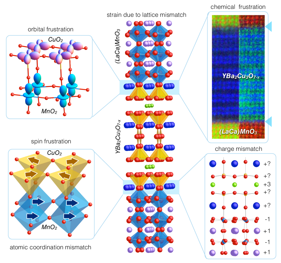
The formation of a coherent perovskite oxide heterointerface, as shown in Figure 1, provides a remarkable correlated electron “playground.” It brings different transition metal cations with their localized electron physics and interacting charge, spin and lattice degrees of freedom into intimate contact in a tunable crystalline environment.
The key structural features of transition metal oxides relate to the coordination geometry of the metal ions and the metal-oxygen-metal bond angles. These determine magnetic exchange interactions Kanamori (1965); Goodenough (1955); Anderson (1950) and electronic bandwidths Eng et al. (2003), thereby controlling the electronic and magnetic ground states. Structural and electronic changes across an interface can act to stabilize previously unanticipated phases of matter Okamoto and Millis (2004).
Consider for example a multilayer heterostructure comprised of alternating blocks of the metallic ferromagnet La2/3Ca1/3MnO3 (LCMO), and the high-temperature cuprate superconductor YBa2Cu3O7-x (YBCO) sketched in Figure 1. The interface brings several crucial structural effects. The first is a coordination mismatch. LCMO is a three-dimensional perovskite (O3 stoichiometry) with corner-connected MnO6 octahedra that may be described by interleaving alternating (La,Ca)O and MnO2 layers along [001]. In contrast, YBCO is a two-dimensional oxide with four- and five-fold coordinated Cu cations. The layered cuprate structure may be considered as a derivative of perovskite, which partly facilitates coherent growth of the heterostructure. But unlike LCMO, YBCO displays an ordered network of oxygen vacancies accommodated by the valence preferences of Cu: One oxygen atom is removed from every third (001) YO plane to produce the square pyramidal CuO5 coordination, then on every third CuO2 layer, vacancies order along [100], producing the square planar CuO4 coordination. Thus a “coordination mismatch” arising from the change from the 6-fold coordination of the Mn to the lower coordination of the Cu (Figure 1, lower left) occurs at the interface. As a result, a set of CuO chains ( charge reservoir) is missing from the interfacial YBCO unit cell to maintain a prerovskite-like sequence …MnO2–BaO–CuO2… across the junction Zhang et al. (2009); Chien et al. (2013).
Coherent epitaxial growth also produces an intrinsic strain mismatch arising from the different equilibrium lattice constants (Figure 1, center). The atomic structure at the heterointerface responds to alleviate the strain mismatch through relaxation of the interatomic distances and internal atomic degrees of freedom (for example, rotations or size deformations to the transition metal oxygen polyhedra) in the constituents along the superlattice repeat direction. These new atomic arrangements directly alter the electronic structure. Away from the interface it is characterized by carriers in the -manifold with orbital symmetries (YBCO) and for LCMO (Figure 1, upper left), but near the interface the become occupied in the YBCO and acquire more character in the LCMO.
In addition to the structural effects, an electronic mismatch occurs. The ferromagnetism in LCMO relies on the cooperative parallel alignment of spins from the narrow correlated electronic bands; singlet Cooper pair formation in YBCO, in contrast, relies on paired spins with antiferromagnetic interactions. These antagonistic spin interactions (frustration) have been invoked to explain changes in the interfacial magnetization and superconductivity, giant magnetoresistance, the appearance of uncompensated magnetic moment on Cu in CuO2 plane, and large modulation of ferromagnetic magnetization profile across the heterojunction Peña et al. (2005); Stahn et al. (2005); Chakhalian et al. (2006); Hoppler et al. (2009)
The different valence configurations of the cations in the constituent materials of the heterostructure also induce changes in charge density and chemical bonding. In the system shown in Figure 1 (lower right panel) a charge of 0.2 per Cu ion is transferred from Mn to Cu ions across the interface Chakhalian et al. (2007). The charge transfer at other oxide interfaces has also been found to exhibit a peculiar asymmetric electronic “roughness” intertwined with an asymmetric interface stacking sequence or an asymmetric chemical roughness Hoffmann et al. (2005); May et al. (2008); Chien et al. (2013). The effects from different stacking sequences and electronic roughness remain to be resolved.
To summarize, the following degrees of freedom are highly tunable at an oxide interface and may be exploited in uncovering new phases:
-
•
Epitaxial strain mismatch owing to differences in equilibrium lattice parameters
-
•
Atomic coordination frustration and cation site preferences
-
•
Ordered spin and orbital states
-
•
Charge flow across the interface (layer dipole discontinuities)
-
•
Chemical frustration and interlayer mixing
The following examples detail how these considerations are made, and the exciting new phases born from the interplay of the correlated electronic and atomic structure across oxide interfaces.
III Charge at the interface
Understanding and controlling the distribution of charge carriers at the interface between dissimilar semiconductors is one of the pivotal developments of modern microelectronics Gertner (2013) important both for devices and as a crucial platform for discovery of remarkable physical phenomena including integer and fractionally quantized Hall effects as well as spin-Hall and other spintronic phenomena.
In conventional semiconductor heterojunctions the basic physics is driven by the difference in work-function, which causes charge transfer across the boundary to equalize chemical potentials. The work-function difference may be manipulated by a process known as -doping Schubert (1990); Harris et al. (1991), in which a layer of ions is implanted in a plane at some distance from the interface. An additional advantage of -doping is that the placement of the dopants at some distance from the interface minimizes the effects of randomness in the dopant positions. -doping is now widely used to produce two dimensional electron gases (2DEGs) confined to the proximity to the interface ( GaAs/AlGaAs).
The interest in using TMO to explore similar physics was motivated by two observations Ahn et al. (2003, 2006): () in oxides, the accessible carrier density is expected to be orders of magnitude higher than that of semiconductors ( cm-3), and () the Thomas-Fermi screening length is expected to be much shorter, so the charges may be confined to within 1-2 nm of the interface, a factor of shorter than the 10 nm length characteristic of semiconductor junctions. However, the current intense effort in material synthesis, theory, and device fabrication of oxide interfaces is motivated mainly by the known sensitivity of the correlated electron properties of transition metal oxides to the -band filling Tokura and Tomioka (1999); Dagotto et al. (2001); Ovchinnikov (2003); Mackenzie (2003); Basov (2005); Lee and Wen (2006); Tokura (2006); Armitage et al. (2010). The discovery of an interface-based method of carrier doping has revived the idea of tailoring the materials electronic properties and creating novel quantum states not easily attainable in the bulk counterparts. The basic idea (analogous to that motivating -doping) is to explore electronic and magnetic phases without the hindering effects of chemical disorder inherent in the conventional solid state chemistry methods of changing carrier concentration.
During the past several years, extensive experimentation has established that perovskite-based heterostructures are particularly susceptible to interlayer charge redistribution derived from the incompatibilities illustrated in Figure 1 making them ideal candidates to explore such possibilities Bibes et al. (2011); May et al. (2009); Okamoto and Millis (2004); Ohtomo and Hwang (2004); Ohtomo et al. (2002).
III.1 Interface Doping of a High- Superconductor
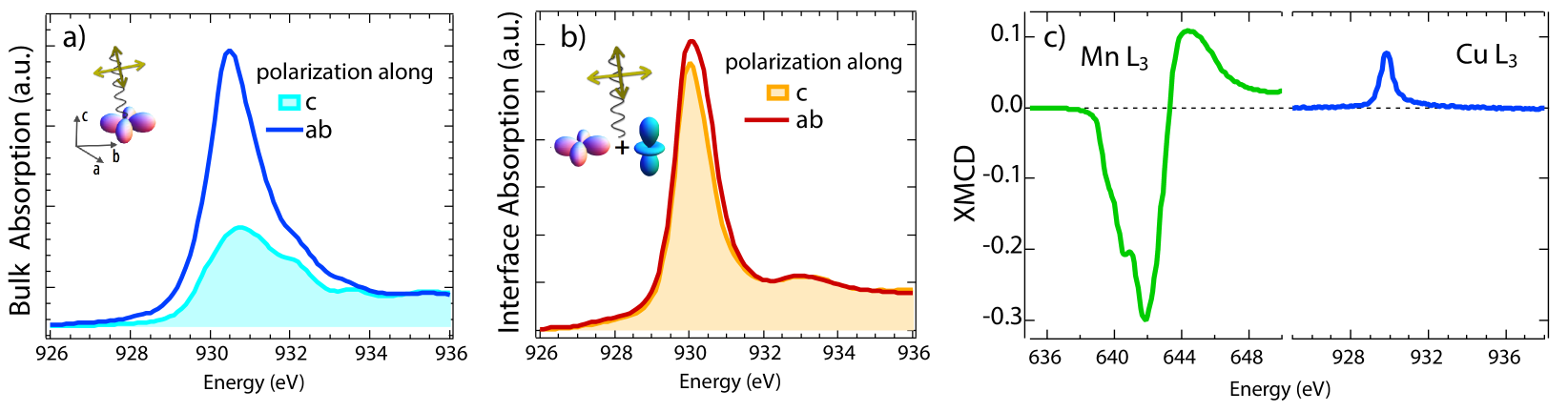
To illustrate the inherent interest of charge reconstruction on interfacial states, we discuss as one of many possible examples the recent progress on cuprate/manganite heterointerfaces. Macroscopically it has been established that the introduction of a ferromagnetic (La,Ca)MnO3 manganite layer into the heterostructure with an optimally doped YBCO cuprate triggers a suppression of the superconducting transition temperature accompanied by a reduced ferromagnetic Curie temperature Satapathy et al. (2012); Driza et al. (2012); Kalcheim et al. (2011); Hoppler et al. (2009); Peña et al. (2004); Holden et al. (2004); Sefrioui et al. (2003). In a recent set of experiments (Figure 2), -edge polarized resonant X-ray absorption spectra taken at the Mn and Cu edges reveal the presence of a chemical shift implying a flow of electronic charge across the interface of about 0.2 per Cu atom Chakhalian et al. (2007); Chien et al. (2013). The depleted electrons from MnO2 layer are directly transferred to the CuO2 planes, unbalancing the charge distribution between the atomic CuO2 layers and the CuO chain charge reservoir block. The average Mn valence also increases from the as-grown value (Mn+3.33) to around 3.5, indicative of covalent bond formation across the Mn–O–Cu interface.
The charge transfer across the interface from the Mn to Cu ions induces a major reconstruction of the -orbital occupancies and frontier orbital symmetries in the interfacial CuO2 layers Chakhalian et al. (2007, 2006). In particular, the Cu orbital, which is fully occupied and electronically inactive in the bulk cuprates becomes active at the interface (Figure 2b). At the same time charge transfer is observed in the presence of enhanced covalent chemical bonding across the interface, the Cu cations from the nominally antiferromagnetic CuO2 plane acquire an uncompensated magnetic moment (Figure 2c), attributed to spin canting of the local moments on the interfacial Cu cations.
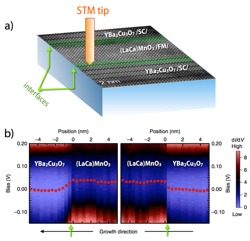
Initial studies of the interplay between the ferromagnetic and superconducting order parameters used synchrotron based X-ray and neutron reflectivity experiments. However these tools were unable to clearly resolve the length scale of interactions at the boundary between the two phases. Very recently, the issue has been addressed by use of cross-sectional scanning tunneling microscopy (XSTM) together with atomic-resolution electron microscopy (EELS/STEM). These methods enable direct observation of the charge distribution and the corresponding spatial scale for the buried interface Chien et al. (2013). Figure 3 shows the spatially resolved / spectra, which provided the first direct evidence that the length scale for charge transfer between YBCO and LCMO has an upper limit of <1 nm, and that the spatial broadening of the electronic transition is commensurate with the rougher interface. This result sets a fundamental upper limit on the charge-transfer length scale in the YBCO/LCMO system, ruling out a class of theories based on long-range proximity effects Hoffmann et al. (2005). In addition to the established X-ray and neutron based probes, this powerful characterization technique provides a useful tool to achieve a microscopic direct space understanding of the electronic structure across correlated oxide interfaces.
III.2 Additional considerations
The complex behavior occurring at the LCMO/YBCO interface highlights the need to develop a clear language and set of concepts to describe interface electronic physics in correlated oxides. The inherently many-body nature of the correlated interface raises fundamental questions, in particular of the applicability of the ideas, formulae, and language devised for semiconductor interfaces where a single-particle description works well. Pioneering work of Oka and Nagaosa Oka and Nagaosa (2005) showed via density matrix renormalization group calculations of a one dimensional model system (in essence the one dimensional Hubbard model with a spatially varying interaction parameter and band bottom) that the standard concepts of band bending and interface dipole apply, albeit with some modifications, as long as the conduction and valence bands are replaced by lower and upper Hubbard bands.
A growing body of literature builds on this work, using the concepts of band bending, Schottky barriers, and depletion layer creation borrowed from semiconductor physics Yajima et al. (2011); Hikita et al. (2009), as well as more involved approaches, which unite Poisson-Schrödinger electrostatics with Mott-Hubbard physics Okamoto and Millis (2004); Charlebois et al. (2013); Lee and Macdonald (2006). Correlation physics is shown to lead to quantitative changes in the spatial confinement of carriers near interfaces Okamoto and Millis (2004); Lee and Macdonald (2006, 2007), including the possible formation of extended depletion regions of zero compressibility (so-called ‘Mott plateaus’)Lee and Macdonald (2006); Charlebois et al. (2013). Other theoretically proposed possibilities unattainable with semiconductor junctions, include a spontaneously emerging quantum-well structure when an electron-doped Mott-Hubbard insulator is coupled to a normal metal with a large work-function. Following the same line of reasoning, in a - junction between two correlated insulators the local Mott gap collapses giving rise to a 2DEG Charlebois et al. (2013).
With few exceptions Jin et al. (2011), current experimental attention has focussed on interfaces such as that between the two band insulators LaAlO3 and SrTiO3. In most of these situations the carriers are introduced via the polar catastrophe mechanism Mannhart et al. (2008); the maximum sheet carrier density is per in-plane unit cell and this carrier density is typically distributed Mannhart et al. (2008); Okamoto et al. (2006) over several unit cells away from the interface, leading in general to volume carrier densities far below the Mott value of one per unit cell. Density functional plus Hubbard calculations Pentcheva and Pickett (2007) indicate that a charge ordered phase in which the entire polar catastrophe charge density is in the first interface layer may be possible, but these suggestions have not yet been confirmed by experiment or beyond-DFT methods. One very interesting potential exception is the work of Moetakef et al., 2012 on GdTiO3/SrTiO3 heterostructures, where a nontrivial insulating phase was observed when two layers of SrTiO3 were sandwiched between thick sheets of GdTiO3. It has been explained by Chen, Lee and Balents in terms of a novel ‘Mott dimer’ phase Chen et al. (2013), where the carrier density is far below the one electron per transition metal ion value needed for Mott physics; nonetheless many theoretical predictions suggest alternative avenues for emergent properties to arise and warrant experimental investigation.
Additional issues beyond conceptual approaches to interface control arise. The length scales in correlated oxides are typically very short, so the details of the interface may be more important than in conventional semiconductors.A local picture is needed, which is able to address the formation of chemical bonds across the junction, differing electronegativities of transition metal ions, changes in both crystal field energies and Madelung potentials, and polarity effects Salluzzo et al. (2013); Garcia-Barriocanal et al. (2013); Park et al. (2013b); Biscaras et al. (2012); Zhong et al. (2010); Savoia et al. (2009); Takizawa et al. (2009); Sing et al. (2009); Herranz et al. (2007); Hotta et al. (2007); Ohtomo and Hwang (2004).
A further complication is that while many correlated oxides are reasonably well described by the Mott-Hubbard picture on which the above-cited works are based, some important functional TMO are charge-transfer compounds Imada et al. (1998); Khomskii and Sawatzky (1997); Zaanen et al. (1985). The role of the lower Hubbard band in these materials is usurped by the ligand states (typically oxygen ), thus implying a very different physical character for the doped holes (mainly in oxygen levels) and doped electrons (mainly in transition metal -levels). As a result, the alignment of the oxygen levels across the interface becomes crucial.
For all of the materials discussed in this paper, theoretical treatments which go beyond the simple Hubbard model, including chemically realistic structures and energetics on the same footing as correlation effects, are needed, as are experimental investigations of systems with higher electron densities and complete control over cation and oxygen stoichiometry.
IV Control of Magnetism with Oxide Heterostructures
Long range magnetic order in transition metal oxides usually arises from a combination of local moment formation on the transition metal site and inter-site coupling via the oxygen sublattice. Heterostructures offer an opportunity to generate new magnetic states by manipulating both the moment formation and the nature of the inter-site coupling. As examples, we note that the paramagnet LaCoO3 can be converted to a ferromagnetic (FM) material by tensile epitaxial strain, which changes the material from a low-spin to a high-spin state Freeland et al. (2008); Park et al. (2009); Rondinelli and Spaldin (2009); Fuchs et al. (2007). On the other hand, bulk antiferromagnetic (AFM) EuTiO3 can be converted to a ferromagnetic insulator under modest tensile strains Lee et al. (2010). Another notable example is the comprehensive study by Seo et al., 2010, which examined three-component SrRuO3/manganite/SrRuO3 heterostructures. These authors found strong compressive strain causes relative FM alignment of magnetization in the heterostructure layers, while tensile or weak compressive strain favors AFM alignment of neighboring layers.
This sort of control over local magnetization in thin film geometries is of potential utility for oxide electronics and spintronic applications, including magnetic memory and sensing Bibes et al. (2011). For example, electromechanical coupling via a piezoelectric material can be used to control the orientation and strength of the magnetization by tuning the lattice parameters of the heterostructure through an applied electric field Dekker et al. (2011). Here, we focus on going beyond strain control to make use of the broken symmetry at the interface between two dissimilar materials to generate unique spatially structured magnetic states.
IV.1 Creating Novel Magnetic States at Interfaces
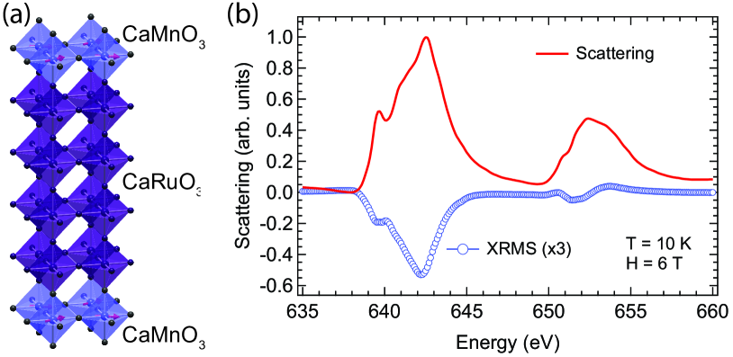
One approach to manipulating magnetism involves interfacial charge transfer in heterostructures created from an antiferromagnetic insulator and a paramagnetic metal Takahashi et al. (2001); Freeland et al. (2010); Yordanov et al. (2011). The choice of materials in this case was determined by two key factors: first, creating moments from a material without any propensity to moment formation, , zero moments, is difficult. It is therefore reasonable to begin then by choosing a system with a large local moment such as CaMnO3 with /Mn, which in bulk is a G-type (conventional two-sublattice Néel) antiferromagnet. However, modest electron doping of this material leads to strong ferromagnetic (FM) correlations Neumeier and Cohn (2000). In a quantum-well heterostructure in which a paramagnetic metal (in this case CaRuO3) is confined between two thick layers of CaMnO3 one may expect that charge transfer from the metal to insulating CaMnO3 will lead to interfacial doping and thus ferromagnetism.
Theoretical studies substantiate this argument and find that a charge of approximately e per interface unit cell leaks across the interface and is confined within 1 unit cell at the CaRuO3/CaMnO3 interface Nanda et al. (2007). Although the magnitude of the charge leakage is small, it has a significant impact on the antiferromagnetic order in the CaMnO3, providing a mechanism for spin canting which yields large ferromagnetic moments at the interface Takahashi et al. (2001); Freeland et al. (2010); Yordanov et al. (2011). To validate this concept a study of the spatial distribution of the magnetism was carried out using X-ray resonant magnetic scattering (XRMS) at the Mn -edge Freeland et al. (2005); Kavich et al. (2007). Figure 4 shows the large XRMS signal, and that it deviates from anticipated bulk G-type AFM state, which shows no ferromagnetic component to the magnetic moment under identical strain conditions indicating that the ferromagnetism emerges from the interface Freeland et al. (2010). By fitting this signal as a function of incident angle, the extent of the magnetic polarization away from the interface was found to extend over several unit cells in contrast to the length of one unit cell predicted by theory Nanda et al. (2007). The observed longer length scale of the magnetization profile discrepancy may be due to magnetic polarons, which are known to exist in lightly-doped CaMnO3 Chiorescu et al. (2007), but such interfacial polarons have not explicitly investigated theoretically.
IV.2 Other Routes to Interface Magnetism
Strain and layer sequencing can offer additional handles to manipulate the interfacial magnetic state in the CaRuO3/CaMnO3 system He et al. (2012). The link between the metallic layer and magnetism is best illustrated by studying superlattices where the metallic layer undergoes a metal-to-insulator transition when the dimensionality is reduced in the ultra-thin layer, and correspondingly the magnetism disappears Grutter et al. (2013). One can use this understanding and exploit it to design new functional materials and there are many possibilities that exist within the perovskite familiy which can be combined to seek new types of magnetic states Smadici et al. (2007); Bhattacharya et al. (2008); Gibert et al. (2012); Hoffman et al. (2013). For example, many antiferromagnets have ordering temperatures well-above room temperature, so one could extend this concept to create interfacial insulating ferrimagnets that operate at high temperature Ueda et al. (1998). Another possibility is to make use of the spatially localized magnetic state in proximity to a metallic layer to create a spin-polarized 2DEG Nanda and Satpathy (2008). More broadly, one could create heterostructures with two magnetic materials, and use the competition towards different collectively ordered magnetic states in addition to structural incompatibilities to generate a plethora of interesting and potentially spatially varying magnetic phases. These are but a few of the magnetic possibilities which remain to be uncovered at oxide heterointerfaces, chosen to highlight the large phase space still available for exploration and the opportunities available to connect with materials theory in the rational search for new magnetic systems.
V Interfacial Control of Orbital Polarization
V.1 The Case of Rare-earth Nickelates
The orbital configuration, , the distribution of the -electrons over the available crystal field levels, plays an important role in the formation of strongly correlated ground states in transition metal oxides Tokura and Nagaosa (2000). In general, orbital configurations are closely linked to structure and may therefore be manipulated at interfaces. Here we discuss these issues specifically for the orthonickelate perovskites NiO3, where is a trivalent cation from the lanthanide series, but the ideas can be extended to other O3 systems.
The original and decade later renewed interest in nickelates arose from the possibility of generating a cuprate-like electronic and orbital configuration in a copper-free system Hamada (1993); Anisimov et al. (1999); Lee and Pickett (2004); Chaloupka and Khaliullin (2008); Poltavets et al. (2010). The basic idea is that in bulk NiO3 the Ni is octahedrally coordinated, with only small deviations from cubic () symmetry. Further, formal valence considerations indicate that the nominally Ni3+ cation is in the low-spin configuration, with the states () filled and one electron in the two-fold degenerate -symmetry () Ni -levels. Low-spin is a first-order Jahn-Teller configuration, with a susceptibility to bond distortions which break the cubic point symmetry and are enhanced by correlation effects. It was thus expected that modest perturbations would split the levels, leaving an effective one-band configuration where the electron is fully confined to a single orbital.
The degree to which an electron occupies two different and orbitals can be quantified as an orbital polarization
where and are the occupancies of the and states Han et al. (2010), with orbital quantum number and magnetic quantum number , respectively. For the rare-earth nickelates, the relevant orbital polarization arises from the and occupancies, and a fully polarized state would be indicative of a single band electronic structure.
Something akin to this effect occurs in many members of the “colossal” magnetoresistance manganites, where the basic configuration is a high-spin configuration and similarly a Jahn-Teller ion that can be manipulated with strain Tokura and Nagaosa (2000). Hubbard-model calculations further indicated that the single-band physics was very likely to appear Hansmann et al. (2009); however, more realistic ab-initio calculations indicate that the actual electronic configuration for Ni is in the high-spin state with a hole on the oxygen () Han et al. (2010). Since the high-spin configuration has one electron in each of the two orbitals, it is significantly less susceptible to undergoing Jahn-Teller distortions, suggesting that it would be more difficult than initially expected to achieve the desired degree of orbital polarization, even in the correlated case Han et al. (2011). Studies of the dependence of orbital polarization on the different flavors of structural symmetry-breaking Cammarata and Rondinelli (2013) is thus of great experimental interest and is a stringent test of the theory.
V.2 Manipulating Orbitals in NiO3 Heterostructures
Advances in high-quality growth of nickelates over the past few years mean that we are now in a position to test these predictions Tsubouchi et al. (2008); Eguchi et al. (2009); Scherwitzl et al. (2010); Liu et al. (2010b); May et al. (2010); Boris et al. (2011); Hwang et al. (2013); Bruno et al. (2013). The basic experimental approach is to use a combination of quantum confinement, achieved by fabricating ultra-thin layers of TMO sandwiched between layers of wide-gap insulators, and epitaxial strain, obtained by varying the substrate material, to break the octahedral symmetry. Advanced x-ray techniques are then used to estimate the resulting changes in orbital occupancies.
However, ab-initio calculations based on density functional theory indicate that the contribution of strain to octahedral symmetry breaking is not completely intuitive (see Rondinelli et al., 2012 and references therein). In particular, a considerable degree of compression or tension can be accommodated by octahedral rotations, without necessarily changing the local point symmetry significantly since the NiO6 units are highly flexible Chakhalian et al. (2011). Furthermore, quantum confinement may be affected by the chemistry of the insulating layer, with different degrees of polarization found for different choices of wide-gap insulator Han et al. (2010).
At present, the experimental results are not completely consistent with each other or with theory. For example, examination of the Ni edge indicated an orbital polarization for a single unit-cell of LaNiO3 subject to tensile strain Freeland et al. (2011) and no orbital polarization for compressive strain. Other measurements employing an orbital reflectometry technique on four unit cell films also observed a similar non-zero interfacial polarization for tensile strain Benckiser et al. (2011); Frano et al. (2013). Recent studies have indicated it is possible to increase the orbital polarization up to through judicious optimization of high tensile strain states and alternative spacer materials Wu et al. (2013); the latter had been shown theoretically to play a considerable role in obtaining the targeted orbital polarization levels Han et al. (2010).
V.3 Open Questions in Orbital Control at Interfaces
All experiments agree though that the degree of orbital polarization observed in actual superlattices is small compared to that needed to achieve a fully orbital polarized Ni state. The main challenge is to then build the framework to understand how to create fully orbital polarized states in oxide heterostructures.
One important facet of this problem has to do with strain and symmetry. For example, LaNiO3 has rhombohedral symmetry in the bulk which actually disfavors a uniaxial Jahn-Teller distortion Carpenter and Howard (2009). NdNiO3, on the other hand, is orthorhombic which allows such a distortion without large energetic penalties. Recent studies by Tung et al., 2013 show that the nickelate films maintain to some extent the symmetry of the bulk, which, due to the connection between compatible lattice distortions and crystal symmetry, directly influences the ability to orbitally polarize the -states even under large strains.
With this understanding, one may be able to choose the proper bulk symmetry of the TMO to be used in the heterostructure to build in larger orbital polarizations in NdNiO3 by coupling strain with the interfacial covalency effect discussed above and interfacial proximity effects Moon et al. (2014); Aso et al. (2014). Even for the case of NdNiO3 films, however, the orbital polarization is still insufficient to create a fully polarized state Tung et al. (2013). This is largely due to the energy scale mismatch between elastic strain ( 100 meV) and the bandwidth (on order of several eV), and the overall tendency to orbital polarization is further reduced by the character of the Ni3+ state.
Small orbital polarizations have also been observed even in the case of the Jahn-Teller active manganites Aruta et al. (2006); Tebano et al. (2008); Pesquera et al. (2012), which indicates that this balancing of drastically different energy scales is difficult even in systems that prefer orbital order. A potential solution is to create interfaces with large symmetry mismatch due to lattice topology or by combination of dissimilar crystal field environments.
Consider for example bulk oxides with large orbital polarization such as the cuprates Nücker et al. (1995); Chen et al. (1992) and Ruddlesden-Popper (layered-structure) nickelates Kuiper et al. (1998); Pellegrin et al. (1996) as a starting point. In these materials, the large orbital polarization arises from the strongly asymmetric crystal (ligand) field of the layered structure. As was discussed above for the LCMO/YBCO heterointerface, oxide interfaces can be harnessed to ‘undo’ orbital polarization, but there is no reason why the converse should not also be possible. This offers a real opportunity in the area of matching systems with drastically different symmetries to create orbital states at the interface.
Orbital control can also be used to modulate strongly correlated states. Strain very effectively controls the metal-insulator transition (MIT) for NdNiO3 thin films Liu et al. (2010a, 2013), but the underlying mechanism is not fully understood. Using quantum confinement when the layer dimensions approach the atomic limit, it was observed that orbital polarization under compressive strain tends to favor a metallic state while quantum confinement caused a re-emergence of a MIT through the interfacial reduction of the orbital polarization Liu et al. (2012a). A similar connection was recently observed in the case of VO2 thin films Aetukuri et al. (2013), where the decrease in the MIT temperature was correlated with strain driven polarization of the V orbitals. The potential use of strain in combination with symmetry mismatch to tune between correlated metallic and insulating phases is an important issue warranting further investigation.
VI Ferroelectric Heterostructures from Nonferroelectric Bulk Oxides
The electrically switchable polarization of ferroelectrics (FE) allows their integration in random access memories (FE-RAM), electro-optical devices, sensing microsystems, active vibration control and surface acoustic wave systems, to high frequency devices Setter et al. (2006). The main challenges for future FE-RAM scaling, however, is that the FE dielectric thickness must be reduced to fit within the required device area while maintaining sufficient reproducibility and signal margins for sense amplifier differentiation between a ‘0’ and ‘1’ data state Wu et al. (2010). Furthermore, non-destructive magnetic sensing of electric polarization, enhanced miniaturization and increased packaging density in magnetoelectric materials (ME) Fiebig (2005); Eerenstein et al. (2006); Ramesh and Spaldin (2007); Velev et al. (2011) would enable the realization of four-state logic in a single device Bibes and Barthelemy (2008); Khomskii (2009).
The conventional approach for realizing strong ME materials, i.e., where their is strong coupling between the primary electric and magnetic polarizations, uses naturally occurring materials possessing primary ferroic orders, namely ferroelectricity and ferromagnetism. Such materials not only are rare, but often suffer from weak coupling between the spin and charge degrees of freedom Eerenstein et al. (2006).
Recent advances in atomic layer epitaxy now enable the design and fabrication of heterostructures with atomically flat interfaces that can support new forms of ferroelectricity Bousquet et al. (2008); Mulder et al. (2013); Rondinelli and Fennie (2012) and magnetoelectric coupling owing to interfacial interactions among electronic spins, charges, and orbitals Wu et al. (2010). A promising avenue to pursue in the search for new materials with emergent ferroelectricity and a strong magnetic field dependence of the electric polarization exploits an superlattice structure with broken inversion symmetry, which results from being constructed from three distinct layers Warusawithana et al. (2003); Lee et al. (2005). The ‘tri-color’ layering lifts inversion symmetry – a prerequisite for an electric polarization – whereas epitaxial strain applied to the heterostructure can promote the formation of electrically and magnetically tunable polarizations, even in the absence of ferroic components Tokura (2007); Hatt and Spaldin (2007).
Using a combination of complementary experimental probes, magnetoelectricity was recently demonstrated in artificial tri-layer heterostructures consisting solely of dielectric antiferromagnetic oxides (Figure 5a). Laser molecular-beam epitaxy was used to create the heterostructure comprising alternating LaMnO3, SrMnO3, NdMnO3 layers on a SrTiO3 substrate. Rogdakis et al., 2012 report the emergence of ferroelectricity below 40K (Figure 5c) and it was found to depend on the number of NdMnO3 layers in the superlattice (Figure 5d). Interestingly, the authors observed slim loop-like polarization–electric (-) field hysteresis, with an extended tail of the polarization above the ferroelectric transition temperature and a thermal hysteresis between zero-field-cooled and field-cooled measurements. Such features are typical of relaxor ferroelectrics and were attributed to interface effects Rogdakis et al. (2012). We note that this dielectric relaxation also leads to differences in the magnitudes of the measured polarization obtained from the - loop and the pyrocurrent measurement, which might also be affected from the challenges in characterizing the dielectric properties of ultrathin film oxides with techniques commonly used for bulk single crystals. Nonetheless, the magnetoelectric coupling resulted in 150% magnetic modulation of the electric polarization, demonstrating how heterostructuring multiple compounds together to lift inversion symmetry in superlattices is an avenue to create new functionalities.
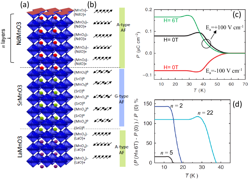
First-principles density functional calculations indicated that broken space inversion symmetry and mixed valency, arising from the heterostructure geometry (cation layer sequence) and interfacial polar discontinuity, respectively, is responsible for the observed behavior. In particular, the formal charge layering of the LaMnO3 and NdMnO3 components at the interfaces with SrMnO3 give rise to a charge discontinuity, leading to electron transfer and cooperative off-centering of the cations. The cation layering leads to a pattern of Mn and -cation displacements along the superlattice normal growth direction that lift inversion symmetry and therefore produce the macroscopic electric polarization. We note that the ferroelectric relaxor behavior could not be seen from the theoretical results, which capture the static and cation ordered zero-temperature behavior.
This work demonstrates yet another fascinating example of emergent functionality exhibited in heterostructures. The ability to lift inversion symmetry and independently tune spin order allows the design of many more materials with multifunctional behavior Puggioni and Rondinelli (2014); Gou and Rondinelli (2014). One may exploit these systems to engineer devices from artificial low-dimensional materials exhibiting novel tunable functions distinct from that of bulk systems.
VII Conclusion
The physics of interfaces between materials exhibiting correlated electronic behaviors including superconductivity, magnetism and ferroelectricity is a rapidly advancing field, situated at the intersection of materials science, solid state chemistry and condensed matter physics. Understanding and exploiting these remarkable systems places extraordinary demands on synthesis, measurement and theory, and the challenge is stimulating remarkable work in all areas. By way of conclusion we highlight challenges and prospects in correlated oxide interfaces.
VII.1 Chemical and structural order
Characterization and control of chemical and structural order is a crucial issue. While research to date has revealed remarkable phenomena, clearly related to properties of theoretically ideal interfaces, effects of disorder are not negligible. The brutally short length scales (often only one or two unit cells) pose strong constraints on materials quality. For example, metal to insulator transitions generically occur in oxide heterstructures when the thickness of the metallic layer becomes of the order of 1-2 unit cells. Systematic dependence on strain Son et al. (2010), and systematic evolution of electronic structure with thickness Yoshimatsu et al. (2011) suggest an important intrinsic component, but disorder effects and changes in growth processes on these length scales cannot yet be ruled out as mechanisms. Antisite defects mean that real interfaces are not as sharp as depicted in the idealized sketches shown in this paper, and these defects are not necessarily easy to identify in transmission electron microscopy experiments, which average over columns of order atoms. Further, oxygen defects and interstitials play a crucial role in transition metal oxides and oxygen partial pressure during growth and in post-growth annealing of heterostructures clearly affects properties in many cases Nakagawa et al. (2006); Ariando et al. (2011). Methods to further define and control the actual structure of interfaces are urgently needed. One area of future study, is to couple the insight from in-situ studies of oxide film synthesis to that of multiscale theory in order to build a mechanistic understanding of the process by which interfaces are created.
VII.2 Theory
The importance and interest of oxide interfaces for the general issue of the theory of correlated electron materials cannot be overemphasized. Understanding the phenomena at interfaces requires a combination of sophisticated many-body physics (to understand the correlated electron states) and ab-initio insights (to understand the implications of the changes in octahedral rotations, atomic coordination, and lattice relaxations). The present state of the theoretical art is a combination of analysis of model systems (in particular the Hubbard model), which cannot easily encode many real materials aspects, in particular the transition-metal/ligand covalence as well as the energetics associated with lattice relaxations and ab-initio techniques (especially the DFT+ method) which have provided crucial insights but are based on a greatly oversimplified Hartree approximation to the many-body physics and may overemphasize order Chan et al. (2009); Wang et al. (2012). In particular the status of the DFT+ predictions of magnetism Okamoto et al. (2006) and charge order Pentcheva and Pickett (2007) at the LAO/STO interface remains unclear.
The combination of density functional band theory and dynamical mean field theory (DFT+DMFT) is a promising alternative Kotliar et al. (2006), combining ab-initio and many-body physics in a systematic way. However, working implementations of total energy calculations are only now beginning to appear Park et al. (2013a) and forces cannot yet be computed so structural optimization remains a challenge. More fundamentally, existing implementations for systems in which more than one -orbital is important are based on the single-site approximation, which is believed to become poor in the two dimensional situation relevant to heterostructures.
VII.3 Topological states of matter
Topological insulators (TIs) are a fascinating class of materials in which strong spin-orbit interaction promotes gapless electronic states on the surface ( edge states) with the bulk of a material remaining gapped Fu et al. (2007); Hsieh et al. (2008); Moore (2010); Qi and Zhang (2010); Hasan and Kane (2010). Most of the current TI materials belong to the Bi (=Se, Te) family. Recently, a new approach has been proposed that is based on superlattices of two (or three) unit cells of a strongly correlated electron perovskite O3 grown along the [111] direction combined with a band insulator spacer layer; the resulting heterostructure structurally forms a buckled honeycomb lattice topologically equivalent to that of graphene lattice for the case of three unit cell strongly correlated oxide. Depending on the strength of electron-electron correlations, magnitude of Hund’s coupling and inter-site hopping, the proposed heterostructures display potentially rich physics associated with exotic electronic and topological phases Rüegg and Fiete (2011); Yang et al. (2011); Xiao et al. (2011); Rüegg et al. (2012); Okamoto (2013); Rüegg et al. (2013). At present, the main challenge in experimental realization is the film growth along the [111] direction since for the commonly used substrates, SrTiO3 LaAlO3, NdGaO3, YAlO3, etc., the (111) structure consists of alternating or charged planes along this direction. The large polar discontinuity generally results in complex surface/interface and electronic reconstructions Enterkin et al. (2010); Marks et al. (2009), which can act to compensate for the polar mismatch. To date there is limited understanding of thin film nucleation, growth and charge compensation in perovskites along highly polar directions. Very recently the synthesis work in this direction has been initiated Middey et al. (2012).
VII.4 Oxygen Defect control
While many of the examples discussed above involve oxygen stoichiometric perovskites, the ease of removal/addition of oxygen can also offer opportunities for materials that can be programmed by their chemical environment Kalinin et al. (2012); Kalinin and Spaldin (2013). While the role of oxygen vacancies has been explored deeply in the context of catalysis and fuel cells Adler (2004), recent work has highlighted the controlled stabilization of related oxygen deficient phases using oxide heterostructures. This is interesting for epitaxial thin film phases such as SrCoO3-δ Jeen et al. (2013b, a) or La1-xSrxFeO3-δ Xie et al. (2013), which can be reversibly converted between oxygen deficient and stoichiometric phases at low temperatures. Since these phases have drastically different ground states, it offers an interesting path for control of strongly correlated electrons via dynamic anion compositional control. By combining low conversion energy with electrochemical gating of vacancies, such as that seen recently for VO2 Jeong et al. (2013) and NiO3 Shi et al. (2013), this approach allows direct control of metal vs. insulating phase as well as possible elements of brain-like (neuromorphic) electronic circuits.
VII.5 Moving beyond the static realm
Up to now, all the properties that have been discussed were limited to the quasi-equilibrium properties, but in the future one should also investigate the dynamical degree of freedom to explore the emergence of unique transient states. While the dynamic response for bulk materials has been extensively investigated Averitt and Taylor (2002); Basov (2005), oxide heterostructures offer new possibilities. Recent pump-probe studies of oxide films illustrate the potential for ultrafast strain modulation Daranciang et al. (2012); Wen et al. (2013), which allows one to manipulate the lattice in a new direction since the film motion is clamped in-plane by epitaxy and can only alter the lattice out of plane. Using this epitaxial constraint allows one to drive the crystalline lattice (symmetry, rotations, etc…) into distinctly different areas of phase space. For example, experiments in manganite thin films showed the emergence of a hidden phase that existed only in the dynamic realm Ichikawa et al. (2011). Moving into the mid-IR region enables direct pumping of lattice modes that can trigger phase transitions Rini et al. (2007) and was recently used to trigger a metal-insulator transition through dynamic strain created by direct pumping of substrate phonons Caviglia et al. (2012). Low energy photons in the THz regime can also serve as a dynamic way to drive transitions with ultra-fast electric fields Liu et al. (2012b). Such experiments have only begun to explore the complex landscape available in the dynamic realm.
Acknowledgements.
Work at Argonne National Laboratory, including the Advanced Photon Source, is supported by the U.S. Department of Energy, Office of Science under grant no. DEAC02-06CH11357. JC was supported by DOD-ARO under grant no. 0402-17291. The work in Singapore was supported by the National Research Foundation, Singapore, through Grant NRF-CRP4-2008-04. JMR was supported by ARO (W911NF-12-1-0133) and acknowledges useful discussions leading to ideas presented in this manuscript during a workshop sponsored by the Army Research Office (grant no. W911NF-12-1-0171). AJM acknowledges the US Department of Energy, Office of Science, under grant No. DE-FG02-04ER46169.References
- Adler (2004) Adler, S. B. (2004), Chemical Reviews 104, 4791.
- Aetukuri et al. (2013) Aetukuri, N. B., A. X. Gray, M. Drouard, M. Cossale, L. Gao, A. H. Reid, R. Kukreja, H. Ohldag, C. A. Jenkins, E. Arenholz, K. P. Roche, H. A. Dürr, M. G. Samant, and S. S. P. Parkin (2013), Nature Physics 9 (10), 661.
- Ahn et al. (2003) Ahn, C. H., J. M. Triscone, and J. Mannhart (2003), Nature 424 (6952), 1015.
- Ahn et al. (2006) Ahn, C. H., M. D. Ventra, J. N. Eckstein, C. D. Frisbie, M. E. Gershenson, A. M. Goldman, I. H. Inoue, J. Mannhart, A. J. Millis, A. F. Morpurgo, D. Natelson, and J.-M. Triscone (2006), Rev. Mod. Phys. 78 (4), 1185.
- Anderson (1950) Anderson, P. (1950), Phys. Rev. 79 (2), 350.
- Anisimov et al. (1999) Anisimov, V., D. Bukhvalov, and T. Rice (1999), Phys. Rev. B 59 (12), 7901.
- Ariando et al. (2011) Ariando,, X. Wang, G. Baskaran, Z. Q. Liu, J. Huijben, J. B. Yi, A. Annadi, A. R. Barman, A. Rusydi, S. Dhar, Y. P. Feng, J. Ding, H. Hilgenkamp, and T. Venkatesan (2011), Nat. Commun. 2, 188.
- Armitage et al. (2010) Armitage, N., P. Fournier, and R. Greene (2010), Rev. Mod. Phys. 82 (3), 2421.
- Aruta et al. (2006) Aruta, C., G. Ghiringhelli, A. Tebano, N. Boggio, N. Brookes, P. Medaglia, and G. Balestrino (2006), Physical Review B 73 (23), 235121.
- Aso et al. (2014) Aso, R., D. Kan, Y. Shimakawa, and H. Kurata (2014), Crystal Growth & Design 0 (0), Article ASAP.
- Averitt and Taylor (2002) Averitt, R. D., and A. J. Taylor (2002), Journal of Physics: Condensed Matter 14 (50), R1357.
- Basov (2005) Basov, D. N. (2005), Rev. Mod. Phys. 77 (2), 721.
- Benckiser et al. (2011) Benckiser, E., M. W. Haverkort, S. Brück, E. Goering, S. Macke, A. Frañó, X. Yang, O. K. Andersen, G. Cristiani, H.-U. Habermeier, A. V. Boris, I. Zegkinoglou, P. Wochner, H.-J. Kim, V. Hinkov, and B. Keimer (2011), Nature Materials 10 (3), 189.
- Bert et al. (2011) Bert, J. A., B. Kalisky, C. Bell, M. Kim, Y. Hikita, H. Y. Hwang, and K. A. Moler (2011), Nat Phys 7 (10), 767.
- Bhattacharya et al. (2008) Bhattacharya, A., S. J. May, S. G. E. te Velthuis, M. Warusawithana, X. Zhai, B. Jiang, J. M. Zuo, M. R. Fitzsimmons, S. D. Bader, and J. N. Eckstein (2008), Phys. Rev. Lett. 100 (25), 257203.
- Bibes and Barthelemy (2008) Bibes, M., and A. Barthelemy (2008), Nature Materials 7 (6), 425.
- Bibes et al. (2011) Bibes, M., J. E. Villegas, and A. Barthelemy (2011), Advances in Physics 60 (1), 5.
- Biscaras et al. (2012) Biscaras, J., N. Bergeal, S. Hurand, C. Grossetête, A. Rastogi, R. C. Budhani, D. Leboeuf, C. Proust, and J. Lesueur (2012), Phys. Rev. Lett. 108 (24), 247004.
- Boris et al. (2011) Boris, A. V., Y. Matiks, E. Benckiser, A. Frano, P. Popovich, V. Hinkov, P. Wochner, M. Castro-Colin, E. Detemple, V. K. Malik, C. Bernhard, T. Prokscha, A. Suter, Z. Salman, E. Morenzoni, G. Cristiani, H. U. Habermeier, and B. Keimer (2011), Science 332 (6032), 937.
- Bousquet et al. (2008) Bousquet, E., M. Dawber, N. Stucki, C. Lichtensteiger, P. Hermet, S. Gariglio, J.-M. Triscone, and P. Ghosez (2008), Nature 452 (7188), 732.
- Brinkman et al. (2007) Brinkman, A., M. Huijben, M. van Zalk, J. Huijben, U. Zeitler, J. C. Maan, W. G. van der Wiel, G. Rijnders, D. H. A. Blank, and H. Hilgenkamp (2007), Nat Mater 6 (7), 493.
- Bruno et al. (2013) Bruno, F. Y., K. Z. Rushchanskii, S. Valencia, Y. Dumont, C. Carrétéro, E. Jacquet, R. Abrudan, S. Blügel, M. Ležaić, M. Bibes, and A. Barthélémy (2013), Physical Review B 88 (19), 195108.
- Cammarata and Rondinelli (2013) Cammarata, A., and J. M. Rondinelli (2013), Phys. Rev. B 87, 155135.
- Carpenter and Howard (2009) Carpenter, M. A., and C. J. Howard (2009), Acta Crystallogr B 65, 134.
- Caviglia et al. (2012) Caviglia, A., R. Scherwitzl, P. Popovich, W. Hu, H. Bromberger, R. Singla, M. Mitrano, M. Hoffmann, S. Kaiser, P. Zubko, S. Gariglio, J.-M. Triscone, M. Först, and A. Cavalleri (2012), Phys. Rev. Lett. 108 (13), 136801.
- Caviglia et al. (2008) Caviglia, A. D., S. Gariglio, N. Reyren, D. Jaccard, T. Schneider, M. Gabay, S. Thiel, G. Hammerl, J. Mannhart, and J. M. Triscone (2008), Nature 456 (7222), 624.
- Chakhalian et al. (2007) Chakhalian, J., J. W. Freeland, H.-U. Habermeier, G. Cristiani, G. Khaliullin, M. van Veenendaal, and B. Keimer (2007), Science 318 (5853), 1114.
- Chakhalian et al. (2006) Chakhalian, J., J. W. Freeland, G. Srajer, J. Strempfer, G. Khaliullin, J. C. Cezar, T. Charlton, R. Dalgliesh, C. Bernhard, G. Cristiani, H. U. Habermeier, and B. Keimer (2006), Nature Physics 2 (4), 244.
- Chakhalian et al. (2011) Chakhalian, J., J. Rondinelli, J. Liu, B. Gray, M. Kareev, E. Moon, N. Prasai, J. Cohn, M. Varela, I. Tung, M. Bedzyk, S. Altendorf, F. Strigari, B. Dabrowski, L. Tjeng, P. Ryan, and J. Freeland (2011), Phys. Rev. Lett. 107 (11), 116805.
- Chaloupka and Khaliullin (2008) Chaloupka, J., and G. Khaliullin (2008), Phys. Rev. Lett. 100 (1), 016404.
- Chan et al. (2009) Chan, C.-K., P. Werner, and A. J. Millis (2009), Phys. Rev. B 80, 235114.
- Charlebois et al. (2013) Charlebois, M., S. R. Hassan, R. Karan, D. Sénéchal, and A.-M. S. Tremblay (2013), Physical Review B 87 (3), 035137.
- Chen et al. (1992) Chen, C., L. Tjeng, J. Kwo, H. Kao, P. Rudolf, F. Sette, and R. Fleming (1992), Phys. Rev. Lett. 68 (16), 2543.
- Chen et al. (2013) Chen, R., S. Lee, and L. Balents (2013), Phys. Rev. B 87, 161119.
- Chien et al. (2013) Chien, T. Y., L. F. Kourkoutis, J. Chakhalian, B. Gray, M. Kareev, N. P. Guisinger, D. A. Muller, and J. W. Freeland (2013), Nature Communications 4, 2336.
- Chiorescu et al. (2007) Chiorescu, C., J. Cohn, and J. Neumeier (2007), Physical Review B 76 (2), 020404.
- Dagotto et al. (2001) Dagotto, E., T. HOTTA, and A. Moreo (2001), Physics Reports 344, 1.
- Daranciang et al. (2012) Daranciang, D., M. Highland, H. Wen, S. Young, N. Brandt, H. Hwang, M. Vattilana, M. Nicoul, F. Quirin, J. Goodfellow, T. Qi, I. Grinberg, D. Fritz, M. Cammarata, D. Zhu, H. Lemke, D. Walko, E. Dufresne, Y. Li, J. Larsson, D. Reis, K. Sokolowski-Tinten, K. Nelson, A. Rappe, P. Fuoss, G. Stephenson, and A. Lindenberg (2012), Phys. Rev. Lett. 108 (8), 087601.
- Dekker et al. (2011) Dekker, M., A. Herklotz, L. Schultz, M. Reibold, K. Vogel, M. Biegalski, H. Christen, and K. Dörr (2011), Phys. Rev. B 84 (5), 054463.
- Driza et al. (2012) Driza, N., S. Blanco-Canosa, M. Bakr, S. Soltan, M. Khalid, L. Mustafa, K. Kawashima, G. Christiani, H.-U. Habermeier, G. Khaliullin, C. Ulrich, M. L. Tacon, and B. Keimer (2012), Nature Materials 11 (8), 675.
- Eerenstein et al. (2006) Eerenstein, W., N. D. Mathur, and J. F. Scott (2006), Nature 442 (7104), 759.
- Eguchi et al. (2009) Eguchi, R., A. Chainani, M. Taguchi, M. Matsunami, Y. Ishida, K. Horiba, Y. Senba, H. Ohashi, and S. Shin (2009), Phys. Rev. B 79 (11), 115122.
- Eng et al. (2003) Eng, H. W., P. W. Barnes, B. M. Auer, and P. M. Woodward (2003), Journal of Solid State Chemistry 175, 94.
- Enterkin et al. (2010) Enterkin, J. A., A. K. Subramanian, B. C. Russell, M. R. Castell, K. R. Poeppelmeier, and L. D. Marks (2010), Nature Materials 9 (3), 245.
- Fiebig (2005) Fiebig, M. (2005), J. Phys. D: Appl. Phys. 38 (8), R123.
- Frano et al. (2013) Frano, A., E. Schierle, M. W. Haverkort, Y. Lu, M. Wu, S. Blanco-Canosa, U. Nwankwo, A. V. Boris, P. Wochner, G. Cristiani, H. U. Habermeier, G. Logvenov, V. Hinkov, E. Benckiser, E. Weschke, and B. Keimer (2013), Phys. Rev. Lett. 111, 106804.
- Freeland et al. (2005) Freeland, J., K. Gray, L. Ozyuzer, P. Berghuis, E. Badica, J. Kavich, H. Zheng, and J. Mitchell (2005), Nature Materials 4 (1), 62.
- Freeland et al. (2010) Freeland, J. W., J. Chakhalian, A. V. Boris, J. M. Tonnerre, J. J. Kavich, P. Yordanov, S. Grenier, P. Zschack, E. Karapetrova, P. Popovich, H. N. Lee, and B. Keimer (2010), Phys. Rev. B 81 (9), 094414.
- Freeland et al. (2011) Freeland, J. W., J. Liu, M. Kareev, B. Gray, J. W. Kim, P. Ryan, R. Pentcheva, and J. Chakhalian (2011), EPL (Europhysics Letters) 96 (5), 57004.
- Freeland et al. (2008) Freeland, J. W., J. X. Ma, and J. Shi (2008), Appl. Phys. Lett. 93 (21), 212501.
- Fu et al. (2007) Fu, L., C. Kane, and E. Mele (2007), Phys. Rev. Lett. 98 (10), 106803.
- Fuchs et al. (2007) Fuchs, D., C. Pinta, T. Schwarz, P. Schweiss, P. Nagel, S. Schuppler, R. Schneider, M. Merz, G. Roth, and H. von Loehneysen (2007), Phys. Rev. B 75 (14), 144402.
- Garcia-Barriocanal et al. (2013) Garcia-Barriocanal, J., A. M. Perez-Muñoz, Z. Sefrioui, D. Arias, M. Varela, C. Leon, S. J. Pennycook, and J. Santamaria (2013), Physical Review B 87 (24), 245105.
- Gertner (2013) Gertner, J. (2013), The Idea Factory: Bell Labs and the Great Age of American Innovation (Penguin, New York, NY).
- Gibert et al. (2012) Gibert, M., P. Zubko, R. Scherwitzl, J. I. niguez, and J.-M. Triscone (2012), Nature Materials 11 (3), 195.
- Goodenough (1955) Goodenough, J. B. (1955), Phys. Rev. 100 (2), 564.
- Gou and Rondinelli (2014) Gou, G., and J. M. Rondinelli (2014), Advanced Materials Interfaces , Early View.
- Granozio et al. (2013) Granozio, F. M., G. Koster, and G. Rijnders (2013), MRS Bulletin 38, 1017.
- Grutter et al. (2013) Grutter, A. J., H. Yang, B. J. Kirby, M. R. Fitzsimmons, J. A. Aguiar, N. D. Browning, C. A. Jenkins, E. Arenholz, V. V. Mehta, U. S. Alaan, and Y. Suzuki (2013), Phys. Rev. Lett. 111, 87202.
- Hamada (1993) Hamada, N. (1993), J. Phys. Chem. Sol. 54, 1157.
- Han et al. (2010) Han, M. J., C. A. Marianetti, and A. J. Millis (2010), Phys. Rev. B 82 (13), 134408.
- Han et al. (2011) Han, M. J., X. Wang, C. A. Marianetti, and A. J. Millis (2011), Phys. Rev. Lett. 107 (20), 206804.
- Hansmann et al. (2009) Hansmann, P., X. Yang, A. Toschi, G. Khaliullin, O. K. Andersen, and K. Held (2009), Phys. Rev. Lett. 103 (1), 016401.
- Harris et al. (1991) Harris, J., J. Clegg, R. Beall, J. Castagné, K. Woodbridge, and C. Roberts (1991), Journal of Crystal Growth 111, 239.
- Hasan and Kane (2010) Hasan, M. Z., and C. L. Kane (2010), Rev. Mod. Phys. 82 (4), 3045.
- Hatt and Spaldin (2007) Hatt, A. J., and N. A. Spaldin (2007), Applied Physics Letters 90 (24), 242916.
- He et al. (2012) He, C., A. Grutter, M. Gu, N. Browning, Y. Takamura, B. Kirby, J. Borchers, J. Kim, M. Fitzsimmons, X. Zhai, V. Mehta, F. Wong, and Y. Suzuki (2012), Phys. Rev. Lett. 109 (19), 197202.
- Herranz et al. (2007) Herranz, G., M. Basletić, M. Bibes, C. Carrétéro, E. Tafra, E. Jacquet, K. Bouzehouane, C. Deranlot, A. Hamzić, J.-M. Broto, A. Barthélémy, and A. Fert (2007), Phys. Rev. Lett. 98 (21), 216803.
- Hikita et al. (2009) Hikita, Y., M. Nishikawa, T. Yajima, and H. Y. Hwang (2009), Phys. Rev. B 79 (7), 073101.
- Hoffman et al. (2013) Hoffman, J., I. C. Tung, B. B. Nelson-Cheeseman, M. Liu, J. W. Freeland, and A. Bhattacharya (2013), Physical Review B 88, 144411.
- Hoffmann et al. (2005) Hoffmann, A., S. T. Velthuis, Z. Sefrioui, J. Santamaría, M. Fitzsimmons, S. Park, and M. Varela (2005), Phys. Rev. B 72 (14), 140407.
- Holden et al. (2004) Holden, T., H.-U. Habermeier, G. Cristiani, A. Golnik, A. Boris, A. Pimenov, J. Humlíc̆ek, O. Lebedev, G. V. Tendeloo, B. Keimer, and C. Bernhard (2004), Phys. Rev. B 69 (6), 064505.
- Hoppler et al. (2009) Hoppler, J., J. Stahn, C. Niedermayer, V. K. Malik, H. Bouyanfif, A. J. Drew, M. Roessle, A. Buzdin, G. Cristiani, H. U. Habermeier, B. Keimer, and C. Bernhard (2009), Nature Materials 8 (4), 315.
- Hotta et al. (2007) Hotta, Y., T. Susaki, and H. Hwang (2007), Phys. Rev. Lett. 99 (23), 236805.
- Hsieh et al. (2008) Hsieh, D., D. Qian, L. Wray, Y. Xia, Y. S. Hor, R. J. Cava, and M. Z. Hasan (2008), Nature 452 (7190), 970.
- Hwang et al. (2012) Hwang, H. Y., Y. Iwasa, M. Kawasaki, B. Keimer, N. Nagaosa, and Y. Tokura (2012), Nature Materials 11 (2), 103.
- Hwang et al. (2013) Hwang, J., J. Son, J. Y. Zhang, A. Janotti, C. G. V. D. Walle, and S. Stemmer (2013), Physical Review B 87 (6), 060101.
- Ichikawa et al. (2011) Ichikawa, H., S. Nozawa, T. Sato, A. Tomita, K. Ichiyanagi, M. Chollet, L. Guerin, N. Dean, A. Cavalleri, S. ichi Adachi, T. hisa Arima, H. Sawa, Y. Ogimoto, M. Nakamura, R. Tamaki, K. Miyano, and S. ya Koshihara (2011), Nature Materials 10 (2), 101.
- Imada et al. (1998) Imada, M., A. Fujimori, and Y. Tokura (1998), Rev. Mod. Phys. 70 (4), 1039.
- Jeen et al. (2013a) Jeen, H., W. S. Choi, M. D. Biegalski, C. M. Folkman, I.-C. Tung, D. D. Fong, J. W. Freeland, D. Shin, H. Ohta, M. F. Chisholm, and H. N. Lee (2013a), Nature Materials 12 (11), 1057.
- Jeen et al. (2013b) Jeen, H., W. S. Choi, J. W. Freeland, H. Ohta, C. U. Jung, and H. N. Lee (2013b), Adv Mater 25, 3651.
- Jeong et al. (2013) Jeong, J., N. Aetukuri, T. Graf, T. D. Schladt, M. G. Samant, and S. S. P. Parkin (2013), Science 339 (6126), 1402.
- Jin et al. (2011) Jin, K., P. Bach, X. H. Zhang, U. Grupel, E. Zohar, I. Diamant, Y. Dagan, S. Smadici, P. Abbamonte, and R. L. Greene (2011), Physical Review B 83 (6), 060511.
- Kalcheim et al. (2011) Kalcheim, Y., T. Kirzhner, G. Koren, and O. Millo (2011), Phys. Rev. B 83 (6), 064510.
- Kalinin et al. (2012) Kalinin, S. V., A. Borisevich, and D. Fong (2012), Acs Nano .
- Kalinin and Spaldin (2013) Kalinin, S. V., and N. A. Spaldin (2013), Science 341 (6148), 858.
- Kanamori (1965) Kanamori, J. (1965), Journal of the Physics and Chemistry of Solids 10, 87.
- Kavich et al. (2007) Kavich, J. J., M. P. Warusawithana, J. W. Freeland, P. Ryan, X. Zhai, R. H. Kodama, and J. N. Eckstein (2007), Phys. Rev. B 76 (1), 014410.
- Khomskii (2009) Khomskii, D. (2009), Physics 2, 20.
- Khomskii and Sawatzky (1997) Khomskii, D., and G. Sawatzky (1997), Solid State Communications 102, 87.
- Kotliar et al. (2006) Kotliar, G., S. Y. Savrasov, K. Haule, et al. (2006), Rev. Mod. Phys. 78 (3), 865.
- Kuiper et al. (1998) Kuiper, P., J. V. Elp, D. Rice, D. Buttrey, H.-J. Lin, and C. Chen (1998), Physical Review B 57 (3), 1552.
- Lee et al. (2005) Lee, H. N., H. M. Christen, M. F. Chisholm, C. M. Rouleau, and D. H. Lowndes (2005), Nature 433 (7024), 395.
- Lee et al. (2010) Lee, J. H., L. Fang, E. Vlahos, X. Ke, Y. W. Jung, L. F. Kourkoutis, J.-W. Kim, P. J. Ryan, T. Heeg, M. Roeckerath, V. Goian, M. Bernhagen, R. Uecker, P. C. Hammel, K. M. Rabe, S. Kamba, J. Schubert, J. W. Freeland, D. A. Muller, C. J. Fennie, P. Schiffer, V. Gopalan, E. Johnston-Halperin, and D. G. Schlom (2010), Nature 466 (7309), 954.
- Lee and Pickett (2004) Lee, K.-W., and W. Pickett (2004), Phys. Rev. B 70 (16), 165109.
- Lee and Wen (2006) Lee, P. A., and X.-G. Wen (2006), Rev. Mod. Phys. 78 (1), 17.
- Lee and Macdonald (2006) Lee, W.-C., and A. Macdonald (2006), Physical Review B 74 (7), 075106.
- Lee and Macdonald (2007) Lee, W.-C., and A. Macdonald (2007), Physical Review B 76 (7), 075339.
- Li et al. (2011) Li, L., C. Richter, J. Mannhart, and R. C. Ashoori (2011), Nat Phys 7, 762.
- Liu et al. (2010a) Liu, J., M. Kareev, B. Gray, J. W. Kim, P. Ryan, B. Dabrowski, J. W. Freeland, and J. Chakhalian (2010a), Appl. Phys. Lett. 96 (23), 233110.
- Liu et al. (2012a) Liu, J., M. Kareev, D. Meyers, B. Gray, P. Ryan, J. Freeland, and J. Chakhalian (2012a), Phys. Rev. Lett. 109 (10), 107402.
- Liu et al. (2010b) Liu, J., M. Kareev, S. Prosandeev, B. Gray, P. Ryan, J. W. Freeland, and J. Chakhalian (2010b), Appl. Phys. Lett. 96 (13), 133111.
- Liu et al. (2013) Liu, J., M. Kargarian, M. Kareev, B. Gray, P. J. Ryan, A. Cruz, N. Tahir, Y.-D. Chuang, J. Guo, J. M. Rondinelli, J. W. Freeland, G. A. Fiete, and J. Chakhalian (2013), Nature Communications 4, 2714.
- Liu et al. (2012b) Liu, M., H. Y. Hwang, H. Tao, A. C. Strikwerda, K. Fan, G. R. Keiser, A. J. Sternbach, K. G. West, S. Kittiwatanakul, J. Lu, S. A. Wolf, F. G. Omenetto, X. Zhang, and K. A. N. R. D. Averitt (2012b), Nature 487, 345.
- Mackenzie (2003) Mackenzie, A. P. (2003), Rev. Mod. Phys. 75 (2), 657.
- Mannhart et al. (2008) Mannhart, J., D. A. Blank, H. Y. Hwang, A. J. Millis, and J. M. Triscone (2008), MRS Bulletin 33, 1027.
- Mannhart and Schlom (2010) Mannhart, J., and D. Schlom (2010), Science 327 (5973), 1607.
- Marks et al. (2009) Marks, L. D., A. N. Chiaramonti, F. Tran, and P. Blaha (2009), Surface Science 603 (14), 2179.
- May et al. (2010) May, S. J., J. W. Kim, J. M. Rondinelli, E. Karapetrova, N. A. Spaldin, A. Bhattacharya, and P. J. Ryan (2010), Phys. Rev. B 82 (1), 014110.
- May et al. (2009) May, S. J., P. J. Ryan, J. L. Robertson, J. W. Kim, T. S. Santos, E. Karapetrova, J. L. Zarestky, X. Zhai, S. G. E. te Velthuis, J. N. Eckstein, S. D. Bader, and A. Bhattacharya (2009), Nature Materials 8 (11), 892.
- May et al. (2008) May, S. J., A. B. Shah, S. G. E. te Velthuis, M. R. Fitzsimmons, J. M. Zuo, X. Zhai, J. N. Eckstein, S. D. Bader, and A. Bhattacharya (2008), Phys. Rev. B 77 (17), 174409.
- Middey et al. (2012) Middey, S., D. Meyers, M. Kareev, E. J. Moon, B. A. Gray, X. Liu, J. W. Freeland, and J. Chakhalian (2012), Applied Physics Letters 101 (26), 261602.
- Moetakef et al. (2012) Moetakef, P., C. A. Jackson, J. Hwang, L. Balents, S. J. Allen, and S. Stemmer (2012), Phys. Rev. B 86, 201102.
- Moon et al. (2014) Moon, E. J., P. V. Balachandran, B. J. Kirby, D. J. Keavney, R. J. Sichel-Tissot, C. M. Schlepütz, E. Karapetrova, X. M. Cheng, J. M. Rondinelli, and S. J. May (2014), Nano Letters 0 (0), Article ASAP.
- Moore (2010) Moore, J. E. (2010), Nature 464 (7286), 194.
- Mulder et al. (2013) Mulder, A. T., N. A. Benedek, J. M. Rondinelli, and C. J. Fennie (2013), Advanced Functional Materials 23 (38), 4810.
- Nakagawa et al. (2006) Nakagawa, N., H. Hwang, and D. Muller (2006), Nature Materials 5 (3), 204.
- Nanda and Satpathy (2008) Nanda, B. R. K., and S. Satpathy (2008), Phys. Rev. Lett. 101 (12), 10.1103/PhysRevLett.101.127201.
- Nanda et al. (2007) Nanda, B. R. K., S. Satpathy, and M. S. Springborg (2007), Phys. Rev. Lett. 98 (21), 216804.
- Neumeier and Cohn (2000) Neumeier, J., and J. Cohn (2000), Physical Review B 61 (21), 14319.
- Nücker et al. (1995) Nücker, N., E. Pellegrin, P. Schweiss, J. Fink, S. Molodtsov, C. Simmons, G. Kaindl, W. Frentrup, A. Erb, and G. Müller-Vogt (1995), Physical Review B 51 (13), 8529.
- Ohtomo and Hwang (2004) Ohtomo, A., and H. Y. Hwang (2004), Nature 427 (6973), 423.
- Ohtomo et al. (2002) Ohtomo, A., D. A. Muller, J. L. Grazul, and H. Y. Hwang (2002), Nature 419 (6905), 378.
- Oka and Nagaosa (2005) Oka, T., and N. Nagaosa (2005), Phys. Rev. Lett. 95 (26), 266403.
- Okamoto (2013) Okamoto, S. (2013), Phys. Rev. Lett. 110, 066403.
- Okamoto et al. (2006) Okamoto, S., A. Millis, and N. Spaldin (2006), Phys. Rev. Lett. 97 (5), 056802.
- Okamoto and Millis (2004) Okamoto, S., and A. J. Millis (2004), Nature 428 (6983), 630.
- Ovchinnikov (2003) Ovchinnikov, S. G. (2003), Phys.-Usp. 46 (1), 21.
- Park et al. (2013a) Park, H., A. J. Millis, and C. A. Marianetti (2013a), arXiv:1310.5772 .
- Park et al. (2013b) Park, J., B.-G. Cho, K. Kim, J. Koo, H. Jang, K.-T. Ko, J.-H. Park, K.-B. Lee, J.-Y. Kim, D. Lee, C. Burns, S. Seo, and H. Lee (2013b), Phys. Rev. Lett. 110 (1), 017401.
- Park et al. (2009) Park, S., P. Ryan, E. Karapetrova, J. W. Kim, J. X. Ma, J. Shi, J. W. Freeland, and W. Wu (2009), Appl. Phys. Lett. 95 (7), 072508.
- Pellegrin et al. (1996) Pellegrin, E., J. Zaanen, H.-J. Lin, G. Meigs, C. Chen, G. Ho, H. Eisaki, and S. Uchida (1996), Physical Review B 53 (16), 10667.
- Peña et al. (2005) Peña, V., Z. Sefrioui, D. Arias, C. Leon, J. Santamaria, J. Martinez, S. T. Velthuis, and A. Hoffmann (2005), Phys. Rev. Lett. 94 (5), 057002.
- Peña et al. (2004) Peña, V., Z. Sefrioui, D. Arias, C. Leon, J. Santamaria, M. Varela, S. Pennycook, and J. Martinez (2004), Phys. Rev. B 69 (22), 224502.
- Pentcheva and Pickett (2007) Pentcheva, R., and W. E. Pickett (2007), Phys. Rev. Lett. 99, 016802.
- Pesquera et al. (2012) Pesquera, D., G. Herranz, A. Barla, E. Pellegrin, F. Bondino, E. Magnano, F. Sánchez, and J. Fontcuberta (2012), Nature Communications 3, 1189.
- Poltavets et al. (2010) Poltavets, V. V., K. A. Lokshin, A. H. Nevidomskyy, M. Croft, T. A. Tyson, J. Hadermann, G. V. Tendeloo, T. Egami, G. Kotliar, N. Aproberts-Warren, A. P. Dioguardi, N. J. Curro, and M. Greenblatt (2010), Phys. Rev. Lett. 104 (20), 206403.
- Puggioni and Rondinelli (2014) Puggioni, D., and J. M. Rondinelli (2014), Nature Communications 5, 3432.
- Qi and Zhang (2010) Qi, X.-L., and S.-C. Zhang (2010), Physics Today 63 (1), 33.
- Ramesh and Spaldin (2007) Ramesh, R., and N. A. Spaldin (2007), Nature Materials 6 (1), 21.
- Reyren et al. (2007) Reyren, N., S. Thiel, A. D. Caviglia, L. F. Kourkoutis, G. Hammerl, C. Richter, C. W. Schneider, T. Kopp, A.-S. Ruetschi, D. Jaccard, M. Gabay, D. A. Muller, J.-M. Triscone, and J. Mannhart (2007), Science 317, 1196.
- Rini et al. (2007) Rini, M., R. Tobey, N. Dean, J. Itatani, Y. Tomioka, Y. Tokura, R. W. Schoenlein, and A. Cavalleri (2007), Nature 449 (7158), 72.
- Rogdakis et al. (2012) Rogdakis, K., J. W. Seo, Z. Viskadourakis, Y. Wang, L. F. N. A. Qune, E. Choi, J. D. Burton, E. Y. Tsymbal, J. Lee, and C. Panagopoulos (2012), Nature Communications 3, 1064.
- Rondinelli et al. (2012) Rondinelli, J., S. May, and J. Freeland (2012), MRS Bulletin 37 (03), 261.
- Rondinelli and Fennie (2012) Rondinelli, J. M., and C. J. Fennie (2012), Advanced Materials 24 (15), 1961.
- Rondinelli and Spaldin (2009) Rondinelli, J. M., and N. A. Spaldin (2009), Phys. Rev. B 79 (5), 054409.
- Rüegg and Fiete (2011) Rüegg, A., and G. Fiete (2011), Phys. Rev. B 84 (20), 201103.
- Rüegg et al. (2012) Rüegg, A., C. Mitra, A. Demkov, and G. Fiete (2012), Phys. Rev. B 85 (24), 245131.
- Rüegg et al. (2013) Rüegg, A., C. Mitra, A. A. Demkov, and G. A. Fiete (2013), Physical Review B 88 (11), 115146.
- Salluzzo et al. (2013) Salluzzo, M., S. Gariglio, X. Torrelles, Z. Ristic, R. D. Capua, J. Drnec, M. M. Sala, G. Ghiringhelli, R. Felici, and N. B. Brookes (2013), Adv Mater 25, 2333.
- Satapathy et al. (2012) Satapathy, D., M. Uribe-Laverde, I. Marozau, V. Malik, S. Das, T. Wagner, C. Marcelot, J. Stahn, S. Brück, A. Rühm, S. Macke, T. Tietze, E. Goering, A. Frañó, J. Kim, M. Wu, E. Benckiser, B. Keimer, A. Devishvili, B. Toperverg, M. Merz, P. Nagel, S. Schuppler, and C. Bernhard (2012), Phys. Rev. Lett. 108 (19), 197201.
- Savoia et al. (2009) Savoia, A., D. Paparo, P. Perna, Z. Ristic, M. Salluzzo, F. M. Granozio, U. S. D. Uccio, C. Richter, S. Thiel, J. Mannhart, and L. Marrucci (2009), Physical Review B 80 (7), 075110.
- Scherwitzl et al. (2010) Scherwitzl, R., P. Zubko, I. G. Lezama, S. Ono, A. F. Morpurgo, G. Catalan, and J.-M. Triscone (2010), Adv. Mater. 22 (48), 5517.
- Schlom et al. (2008) Schlom, D. G., L.-Q. Chen, X. Pan, A. Schmehl, and M. A. Zurbuchen (2008), J Am Ceram Soc 91 (8), 2429.
- Schubert (1990) Schubert, E. F. (1990), Journal of Vacuum Science & Technology A 8 (3), 2980.
- Sefrioui et al. (2003) Sefrioui, Z., D. Arias, V. Peña, J. Villegas, M. Varela, P. Prieto, C. León, J. Martinez, and J. Santamaria (2003), Physical Review B 67 (21), 214511.
- Seo et al. (2010) Seo, J. W., W. Prellier, P. Padhan, P. Boullay, J.-Y. Kim, H. Lee, C. D. Batista, I. Martin, E. E. M. Chia, T. Wu, B.-G. Cho, and C. Panagopoulos (2010), Phys. Rev. Lett. 105 (16), 167206.
- Setter et al. (2006) Setter, N., D. Damjanovic, L. Eng, G. Fox, S. Gevorgian, S. Hong, A. Kingon, H. Kohlstedt, N. Y. Park, G. B. Stephenson, I. Stolitchnov, A. K. Taganstev, D. V. Taylor, T. Yamada, and S. Streiffer (2006), J. Appl. Phys. 100 (5), 051606.
- Shi et al. (2013) Shi, J., S. D. Ha, Y. Zhou, F. Schoofs, and S. Ramanathan (2013), Nature Communications 4, 2676.
- Sing et al. (2009) Sing, M., G. Berner, K. Goß, A. Müller, A. Ruff, A. Wetscherek, S. Thiel, J. Mannhart, S. A. Pauli, C. W. Schneider, P. R. Willmott, M. Gorgoi, F. Schäfers, and R. Claessen (2009), Phys. Rev. Lett. 102 (17), 10.1103/PhysRevLett.102.176805.
- Smadici et al. (2007) Smadici, S., P. Abbamonte, A. Bhattacharya, X. Zhai, B. Jiang, A. Rusydi, J. N. Eckstein, S. D. Bader, and J.-M. Zuo (2007), Phys. Rev. Lett. 99 (19), 196404.
- Son et al. (2010) Son, J., P. Moetakef, J. M. Lebeau, D. Ouellette, L. Balents, S. J. Allen, and S. Stemmer (2010), Appl. Phys. Lett. 96 (6), 062114.
- Stahn et al. (2005) Stahn, J., J. Chakhalian, C. Niedermayer, J. Hoppler, T. Gutberlet, J. Voigt, F. Treubel, H.-U. Habermeier, G. Cristiani, B. Keimer, and C. Bernhard (2005), Physical Review B 71 (14), 140509.
- Takahashi et al. (2001) Takahashi, K. S., M. Kawasaki, and Y. Tokura (2001), Applied Physics Letters 79 (9), 1324.
- Takizawa et al. (2009) Takizawa, M., Y. Hotta, T. Susaki, Y. Ishida, H. Wadati, Y. Takata, K. Horiba, M. Matsunami, S. Shin, M. Yabashi, K. Tamasaku, Y. Nishino, T. Ishikawa, A. Fujimori, and H. Y. Hwang (2009), Phys. Rev. Lett. 102 (23), 10.1103/PhysRevLett.102.236401.
- Tebano et al. (2008) Tebano, A., C. Aruta, S. Sanna, P. Medaglia, G. Balestrino, A. Sidorenko, R. D. Renzi, G. Ghiringhelli, L. Braicovich, V. Bisogni, and N. Brookes (2008), Phys. Rev. Lett. 100 (13), 137401.
- Tokura (2006) Tokura, Y. (2006), Rep Prog Phys 69 (3), 797.
- Tokura (2007) Tokura, Y. (2007), Journal of Magnetism and Magnetic Materials 310, 1145.
- Tokura and Nagaosa (2000) Tokura, Y., and N. Nagaosa (2000), Science 288 (5465), 462.
- Tokura and Tomioka (1999) Tokura, Y., and Y. Tomioka (1999), Journal of Magnetism and Magnetic Materials 200, 1.
- Tsubouchi et al. (2008) Tsubouchi, K., I. Ohkubo, H. Kumigashira, Y. Matsumoto, T. Ohnishi, M. Lippmaa, H. Koinuma, and M. Oshima (2008), Appl. Phys. Lett. 92 (26), 262109.
- Tung et al. (2013) Tung, I. C., P. V. Balachandran, J. Liu, B. A. Gray, E. A. Karapetrova, J. H. Lee, J. Chakhalian, M. J. Bedzyk, J. M. Rondinelli, and J. W. Freeland (2013), Physical Review B 88 (20), 205112.
- Ueda et al. (1998) Ueda, K., H. Tabata, and T. Kawai (1998), Science 280 (5366), 1064.
- Velev et al. (2011) Velev, J. P., S. S. Jaswal, and E. Y. Tsymbal (2011), Philosophical Transactions of the Royal Society A: Mathematical, Physical and Engineering Sciences 369 (1948), 3069.
- Wang et al. (2012) Wang, X., M. J. Han, L. de’ Medici, H. Park, C. A. Marianetti, and A. J. Millis (2012), Phys. Rev. B 86, 195136.
- Warusawithana et al. (2003) Warusawithana, M. P., E. V. Colla, J. N. Eckstein, and M. B. Weissman (2003), Phys. Rev. Lett. 90 (3), 036802.
- Wen et al. (2013) Wen, H., P. Chen, M. Cosgriff, D. Walko, J. Lee, C. Adamo, R. Schaller, J. Ihlefeld, E. Dufresne, D. Schlom, P. Evans, J. Freeland, and Y. Li (2013), Phys. Rev. Lett. 110 (3), 037601.
- Wu et al. (2013) Wu, M., E. Benckiser, M. W. Haverkort, A. Frano, Y. Lu, U. Nwankwo, S. Brück, P. Audehm, E. Goering, S. Macke, V. Hinkov, P. Wochner, G. Christiani, S. Heinze, G. Logvenov, H.-U. Habermeier, and B. Keimer (2013), Physical Review B 88 (12), 125124.
- Wu et al. (2010) Wu, S. M., S. A. Cybart, P. Yu, M. D. Rossell, J. X. Zhang, R. Ramesh, and R. C. Dynes (2010), Nature Materials 9 (9), 756.
- Xiao et al. (2011) Xiao, D., W. Zhu, Y. Ran, N. Nagaosa, and S. Okamoto (2011), Nature Communications 2, 596.
- Xie et al. (2013) Xie, Y., M. D. Scafetta, R. J. Sichel-Tissot, E. J. Moon, R. C. Devlin, H. Wu, A. L. Krick, and S. J. May (2013), Adv Mater , n/a.
- Yajima et al. (2011) Yajima, T., Y. Hikita, and H. Y. Hwang (2011), Nature Materials 10 (3), 198.
- Yang et al. (2011) Yang, K.-Y., W. Zhu, D. Xiao, S. Okamoto, Z. Wang, and Y. Ran (2011), Phys. Rev. B 84 (20), 201104.
- Yordanov et al. (2011) Yordanov, P., A. Boris, J. Freeland, J. Kavich, J. Chakhalian, H. Lee, and B. Keimer (2011), Phys. Rev. B 84 (4), 045108.
- Yoshimatsu et al. (2011) Yoshimatsu, K., K. Horiba, H. Kumigashira, T. Yoshida, A. Fujimori, and M. Oshima (2011), Science 333 (6040), 319.
- Zaanen et al. (1985) Zaanen, J., G. Sawatzky, and J. Allen (1985), Phys. Rev. Lett. 55 (4), 418.
- Zhang et al. (2009) Zhang, Z. L., U. Kaiser, S. Soltan, H.-U. Habermeier, and B. Keimer (2009), Appl. Phys. Lett. 95 (24), 242505.
- Zhong et al. (2010) Zhong, Z., P. X. Xu, and P. J. Kelly (2010), Physical Review B 82 (16), 165127.
- Zubko et al. (2011a) Zubko, P., S. Gariglio, M. Gabay, P. Ghosez, and J.-M. Triscone (2011a), Annual Review Of Condensed Matter Physics 2, 141.
- Zubko et al. (2011b) Zubko, P., S. Gariglio, M. Gabay, P. Ghosez, and J. M. Triscone (2011b), in Annual Review of Condensed Matter Physics, Vol 2, Annual Review of Condensed Matter Physics, Vol. 2, edited by J. S. Langer (Annual Reviews, Palo Alto) pp. 141–165.