Coulomb blockade with neutral modes
Abstract
We study transport through a quantum dot in the fractional quantum Hall regime with filling factors and , weakly coupled to the leads. We account for both injection of electrons to/from the leads, and quasiparticle rearrangement processes between the edge and the bulk of the quantum dot. The presence of neutral modes introduces topological constraints that modify qualitatively the features of the Coulomb blockade (CB). The periodicity of CB peak spacings doubles and the ratio of spacing between adjacent peaks approaches (in the low temperature and large dot limit) a universal value: for and for . The corresponding CB diamonds alternate their width in the direction of the bias voltage and allow for the determination of the neutral mode velocity, and of the topological numbers associated with it.
pacs:
Coulomb blockade (CB) conductance oscillations in small quantum Hall islands is proven to be a useful tool to study the structure of the edge modes. Early experiments McEuen ; Foxman performed in the integer quantum Hall effect (QHE) regime were instrumental to demonstrate the presence of compressible and incompressible stripes along the edge Shklovskii ; Beenakker . Various generalizations to tunneling through a quantum dot in the fractional quantum Hall regime have been proposed Maksym ; Kinaret .
More recent effort has been focused on the nature and structure of the fractional QHE edges at composite filling factors such as Meir ; Beenakker92 ; Heiblum2010 ; Yacoby ; Heiblum , Heiblum2010 ; Yacoby-1 ; Smet ; Akhmerov , and other filling fractions Hiro . Early models of the edge Beenakker92 posited that the current is carried by two edge channels, each having the characteristics of a edge state. Other models MacDonald introduced counter-propagating edge channels corresponding to and . These models yield a Hall conductance which is not quantized and is non-universal, and do not explain certain experimental facts Wang . Following Wen’s Wen description of the fractional QHE edge Kane, Fisher and Polchinski considered the composite edge KFP . They showed that the two original counter-propagating modes are strongly mixed by both disorder and inter-mode interaction. Under fairly general conditions such mixing results in the emergence of a forward charge mode along with a backward moving neutral mode. The latter carries energy (heat), but no electric charge. While neutral modes have been detected in various setups Heiblum2010 ; Yacoby ; Hiro , understanding the full implications of the physics involved, and characterising their topological numbers, remains a major challenge. This task gained significant urgency since the structure of the edge modes provides an insight into the possible non-Abelian nature of the anti-Pfaffian state MooreRead ; ReadGreen , explored for quantum information purposes Nayak .
It was suggested Grosfeld that the pattern of the CB peaks as well as thermopower measurements Stern in a QHE island with the composite filling fraction may be used to detect the presence of neutral modes. In particular it has been argued that CB peak spacing exhibits a slight period doubling in state Meir ; Stern ; Shklovskii . A more complicated modulation of CB peak structure was predicted for other fractions Parsa , including (the structure will then depend on the exact nature of the ground state MooreRead ; ReadGreen ; Lee ; Levin ).
The present paper focuses on the structure of CB diamonds (i.e. non-linear source-drain conductance) along with the peak spacing in composite fraction QHE dots. As opposed to previous studies, here we study the direct consequences of quasiparticle exchange between the edge and the bulk of the quantum dot. Our main findings are: (i) We show that, under rather general assumptions regarding the electrostatic energies of the dot, such edge-bulk exchange leads to a distinct universal pattern of CB diamonds as well as peak spacing. In particular, we find that for the CB peak spacing tends to a universal ratio between odd and even states in the limit of large dot. At the same time the Coulomb diamonds are wider in the source-drain voltage directions (i.e. larger gap) between closely spaced peaks and narrower (i.e. smaller gap) between remotely spaced peaks, Fig. 3. (ii) The width of the Coulomb diamonds in the source-drain bias provides a direct information on the velocity of the neutral modes, and consequently on the topological numbers (so-called zero modes) associated with the latter. (iii) We carry a similar analysis for systems. Assuming an anti-Pfaffian state MooreRead ; Levin , we find a tendency (in the limit of large dot) towards a universal ratio between odd and even states, and a similar (though distinct) pattern of CB diamonds as well.
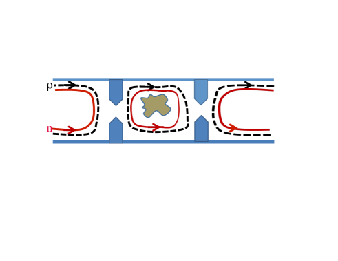
Consider an (almost) isolated 2D island of QHE liquid confined by electrostatic gates McEuen , Fig. 1. It contains an integer number of electrons . If the external magnetic field is such that the Landau level filling factor is a fraction, e.g. , the bulk of the dot has a correlated ground state separated from the excitation spectrum by a gap. The only low energy excitations are those localized along the edge Wen ; KFP . There may be more than one type of such edge excitations having different charges and velocities Meir . For a macroscopic sample all edge modes are gapless, while for a closed dot they acquire a small gap which scales as , where is the mode velocity, is its scaling dimension and is the radius (or rather circumference) of the dot. Imagine now varying the gate voltage, thus increasing the effective area of the dot and consequently the number of flux quanta penetrating it. Provided the number of electrons, , remains unchanged, this would decrease the filling factor . As a result, it either creates fractionally charged quasiparticle (actually quasihole) excitations in the bulk of the dot or on its edge Grosfeld . Which of the two is favorable depends on the ratio between the charging energy of a quasiparticle in the bulk, and the edge gap mentioned above. An important observation is that this balance depends on the gate voltage and may ubruptly flip upon an adiabatic variation of the latter. This is the mechanism of the quasiparticle exchange between the bulk and the edge at fixed , central to our discussion.
Upon further variation of the gate voltage, it may become energetically favorable to move one electron from the lead to the dot. If two leads are attached, Fig. 1, a current may flow through the dot under a small source–drain voltage. This is reflected in a sharp rise of the linear conductance at certain gate voltages, known as CB peaks. It is important to notice that it is an electron, and not a fractionally charged quasiparticle, which is exchanged between the dot and the leads. The positions of the CB peaks are sensitive to the energy cost of accommodating an additional electron. The latter depends on the way the electron is decomposed onto fractionally charged edge modes and bulk quasiparticles.
To be specific, consider a quantum dot in the QHE regime. If the dot is sufficiently large, disorder and interactions lead to the formation of charge and neutral modes KFP , described by the bosonic fields and correspondingly (the charge density is given by ). Under these conditions, the elementary edge excitations are given by a triplet of quasiparticles and a doublet of electrons, described by the operators KFP ; Stern
| (1) | |||
where we have indicated the corresponding electric charge, , and the scaling dimension . The indices in are quantum numbers of the neutral modes, classified according to representations of algebra KFP . The operators are responsible for exchange of the quasiparticles between the bulk and the edge of the dot, while the operators create an electron (which is injected from the leads) at the edge.
The state of the dot may be characterized by three numbers : the integer net number of electrons, , which have tunneled to the edge from the lead(s), the charge, , which is moved to the edge from the bulk (equals to an integer times one third), and the number of neutral (zero mode) excitations at the edge (we will consider ). The energy of the dot is thus given by
| (2) |
where is the bulk charging energy, is dimensionless gate voltage and is the velocity of the charge/neutral edge mode, . Hereafter we shall assume that the bulk charging energy and neutral mode gap is smaller than the kinetic energy of the charge mode . This is the case, if the linear size of the dot is larger than its distance to the gate, : the dot capacitance is . In writing Eq. (2) we have also assumed that the gate is much more strongly coupled to the edge, than to the bulk of the dot. This is indeed the case in most experimental setups.
At some gate voltage, hereafter taken to be , the ground state of the dot is labeled as . Upon varying the gate voltage, , the energy of the dot increases quadratically as – the (black) parabola centered at in Fig. 2– denoted as . One may expect that the ground state follows this parabola until it becomes energetically favorable to move an electron from the lead to the edge, utilizing, say, the operator . This would bring the dot to the state - the (blue) parabola centered at . The crossing between these two parabolas, marked by a (purple) square, takes place at at a rather high energy of the order . According to this logic Stern , the next time electron tunnels it is with the aid of at , bringing the system to the state - the (green) parabola centered at . This state is equivalent to the initial , with two added electrons. As a result the CB periodicity corresponds to two electrons, as first realized in Ref. Meir . The odd-even peak spacing modulation scales as , and is expected to be small Stern .
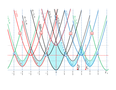
We note, however, that quasiparticle exchange between the edge and the bulk qualitatively modifies the sequence outlined above. Starting again from the state and varying the gate voltage voltage , one arrives at the point where moving one quasiparticle from the bulk to the edge becomes advantageous. Removing a quasiparticle from the edge is achieved with the aid of operators such as . The latter brings the system to the state . We note that this change of the system’s ground state involving edge-bulk charge rearrangement can be observed using a sensitive charge detector. Since in all experiments the gate voltage is varied adiabatically, the system is bound to follow its lowest energy state, which involves such quasiparticles exchange. Following the state, the system arrives at the point (a (blue) circle in Fig. 2), where an electron enters from the lead ( is changed by ), while a charge quasiparticle returns into the bulk. The corresponding composite operator brings the system into the state . It does have an additional electron, but contrary to the scenario outlined above, does not involve neutral mode excitation. As a result, the only energy to pay is for a charge in the bulk, which is the smallest energy scale here. The system then proceeds through a sequence of states which differ by quasiparticle rearrangements between the bulk and the edge. First to the state with the aid of , then to state with the aid of . Only then it becomes advantageous to bring in yet another electron from the lead and return quasiparticle to the bulk with the composite operator , making a transition to the state . Finally moving another quasiparticle from the bulk with , the cycle is complete, and the system arrives at the state.
Once again, the CB period is two electrons, in agreement with Refs. Meir ; Stern . The CB peaks however are positioned at markedly different locations vis-a-vis the gate voltage variation. In the limit the latter tend to . Hence, one approaches the universal ratio of odd–even CB peak spacings. One may argue that, since the electron tunneling is now accompanied by edge-bulk rearrangement, the peak conductance scales as a higher power of temperature and is rather small. While this is a valid argument, notice that, upon adiabatic tuning of the gate voltage, the system has no choice, but to follow its true ground state. Thus the only CB peaks which may be ever observed are those where the ground state changes its number of electrons by one. Although the source-drain conductance happens to be small at this location, no other CB peaks could be reached in an adiabatic measurement.
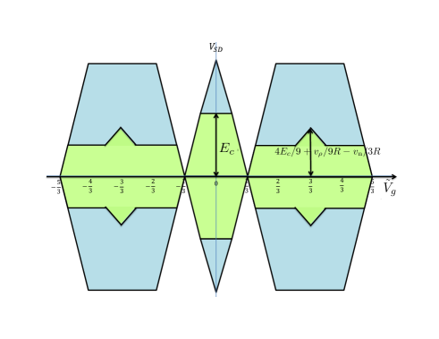
Possibly more interesting than the peak spacing, are the characteristics of the CB diamonds. The latter are observed in the non-linear regime upon the application of a finite source–drain voltage . For a fixed gate voltage away from a CB peak, say , the linear source–drain conductance is exceedingly small. It stays small until reaches the energy of an excited state which differs from the ground state by the addition of one electron. For the simplest of such excited state has a rather high energy . However, there are other excited states contributing to nonlinear source–drain conductance at substantially smaller voltage . In addition to electron tunneling from the lead, they involve bulk-edge exchange of quasiparticles. Examples of such states are , and . The latter (with energy ) is the lowest excited state. The energy difference between the (dashed blue) (or (dashed red)) lowest excited state and the (black) ground state (shown in blue shade) corresponds to the range of with vanishing differential conductance (cf. Fig. 3), i.e. a CB diamond. For -even ground states, i.e. between narrowly spaced CB peaks, the source-drain width of the diamond is about the bulk charging energy, . Let us turn now to the regions of -odd ground state, e.g. (blue). The current carrying excitations are now states with and . It easy to see that the lowest energy ones are (dashed black) and (dashed green). Their excitation energy in the middle of the diamond, i.e. , is , typically smaller than in -even ground states. The width of the small triangles centered around is . One can therefore determine all three energy scales , and from the shape of CB diamonds.
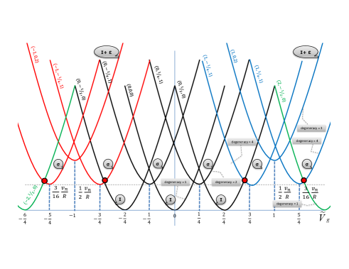
We now briefly outline details and results of a similar analysis for the anti-Pfaffian (APF) state Grosfeld ; Rosenow+08 ; Rosenow+09 ; Parsa , believed to be a candidate for the ground state of the fraction Lee ; Levin . Due to its non-Abelian nature the electron and quasiparticle operators carry Klein factors, , Kitaev ; Law with non-trivial fusion rules. These factors select possible sequence of transitions which an initial ground-state may undergo upon changing the gate voltage along with the degeneracy of corresponding states Bonderson. The corresponding set of the operators is
| (3) | |||
supplemented by the fusion rules: , and .
Upon varying the gate voltage the initial ground state, labeled as and , gives way to the internally rearranged double-degenerate state , Fig. 4, obtained by transferring quasiparticle to the bulk with the operator . The latter is succeeded by non-degenerate state , obtained by moving yet another quasiparticle with the operator . Only then it is energetically favorable to bring an external electron and move another quasiparticle with the help of either , or , leading to 4 times degenerate state. This marks the position of the first CB peak. The cycle is then completed by successively moving two more quasiparticles to the bulk by going through and . The latter then allows to bring the second electron and to move back a quasiparticle, arriving at state . This completes the two electron periodicity cycle. As seen in Fig. 4, the distance between successive CB peaks approaches a ratio. Similarly to the case, the corresponding CB diamonds are narrow in the source drain direction in between the distant CB peaks and wider in between the closely spaced peaks.
To conclude, we have analyzed CB in quantum dots with composite structure of the edge modes. We have shown that the presence of neutral modes leads to distinct features visible both in linear and non-linear conductance measurements. In particular, the sequence of linear response CB peaks exhibits double periodicity with the universal peak distance ratio. The shape and size of non-linear CB diamonds, on the other hand, offer a way to measure edge modes velocities for both charge and neutral edge excitations.
Acknowledgements.
We thank Eytan Grosfeld, Moty Heiblum, Yigal Meir and Ady Stern for illuminating discussions and Parsa Bonderson for very useful correspondence. AK was supported by NSF grant DMR1306734. YG was supported by grants from the German-Israel Foundation, from BSF, and DFG grant RO 2247/8-1.References
- (1) P. L. McEuen, et al, Phys. Rev B 45, 11419 (1992); P. L. McEuen, et al, Physica B 189, 70 (1993).
- (2) E. B. Foxman, et al, Phys. Rev B 47, 10020 (1993).
- (3) D. B. Chklovskii, B. I. Shklovskii, and L. I. Glazman, Phys. Rev. B 46, 4026 (1992).
- (4) A. M. Chang and J. E. Cunningham, Phys. Rev. Lett. 69, 2114 (1992); C. W. J. Beenakker, Phys. Rev. Lett. 64, 216 (1990).
- (5) P. A. Maksym and T. Chakraporty, Phys. Rev. Lett. 65, 108 (1990); T. P. Smith, Surface Science 229, 239 (1990).
- (6) J. M. Kinaret, Y. Meir, N. S. Wingreeen, P. A. Lee, and X-G Wen, Phys. Rev. B 46, 4681 (1992).
- (7) J. M. Kinaret, Y. Meir, N. S. Wingreen, P. Lee, and X-G. Wen, Phys. Rev. B 45, 9489 (1992).
- (8) I. K. Marmorkos and C. W. J. Beenakker, Phys. Rev. B 46, 15562 (1992).
- (9) A. Bid, N. Ofek, H. Inoue, M. Heiblum, C. Kane, V. Umansky, and D. Mahalu, Nature 466, 585 (2010).
- (10) V. Venkatachalam, S. Hart, L. Pfeiffer, K. West, and A. Yacoby, Nat. Phys. 8, 676 (2012).
- (11) I. Gurman, R. Sabo, M. Heiblum, V. Umansky and D. Mahalu, Nature Communications 3, 1289 (2012).
- (12) V. Venkatachalam, A. Yacoby, L. Pfeiffer, and K. West, Nature 469, 185 (2011).
- (13) J. Nuebler, B. Friess, V. Umansky, B. Rosenow, M. Heiblum, K. v. Klitzing, and J. Smet, Phys. Rev. Lett. 108, 046804 (2012).
- (14) B. van Heck, M. Burrello, A. Yacoby, and A. R. Akhmerov, Phys. Rev. Lett. 110, 086803 (2013).
- (15) H. Inoue, A. Grivnin, Y. Ronen, M. Heiblum, V. Umansky, and D. Mahalu, Nat. Commun. 5, 4067 (2014); H. Inoue, A. Grivnin, N. Ofek, I. Neder, M. Heiblum, V. Umansky, and D. Mahalu, Phys. Rev. Lett. 112, 166801 (2014).
- (16) S. M. Girvin, Phys. Rev. B 29, 6012 (1984); A. H. MacDonald, Phys. Rev. Lett. 64, 220 (1990).
- (17) J. Wang, Y. Meir, and Y. Gefen, Phys. Rev. Lett. 111, 246803 (2013).
- (18) X. G. Wen, Phys. Rev. B 43, 11025 (1991); Phys. Rev. Lett. 64, 2206 (1990); Phys. Rev. B 44, 5708 (1991).
- (19) C. L. Kane, M. P. A. Fisher, and J. Polchinski, Phys. Rev. Lett. 72, 4129 (1994); C. L. Kane and M. P. A. Fisher, Phys. Rev. B 51, 13449 (1995).
- (20) G. Moore and N. Read, Nucl. Phys. B 360, 362 (1991).
- (21) N. Read and D. Green, Phys. Rev. B 61, 10267 (2000).
- (22) C. Nayak, S. H. Simon, A. Stern, M. Freedman, and S. Das Sarma, Rev. Mod. Phys. 80, 1083 (2008).
- (23) R. Ilan, E. Grosfeld, and A. Stern, Phys. Rev. Lett. 100, 086803 (2008); R. Ilan, E. Grosfeld, K. Schoutens, and A. Stern, Phys. Rev. B 79, 245305 (2009).
- (24) G. Viola, S. Das, E. Grosfeld, and A. Stern, Phys. Rev. Lett. 109, 146801 (2012).
- (25) For another mechanism of CB period modulation see: A. A. Koulakov and B. I. Shklovskii, Phys. Rev. B 57, 2352 (1998).
- (26) P. Bonderson, C. Nayak, K. Shtengel, Phys. Rev. B 81, 165308 (2010).
- (27) S.-S. Lee, S. Ryu, C. Nayak, and M. P. A. Fisher, Phys. Rev. Lett. 99, 2368071 (2007).
- (28) M. Levin, B. I. Halperin, B. Rosenow, Phys. Rev. Lett. 99, 236806 (2007).
- (29) In the present discussion we have neglected cotunneling dominated transport, which is small and involves high order terms of electron and quasiparticle operators. This will be discussed elsewhere.
- (30) B. Rosenow, B.I. Halperin, S.H. Simon, and A. Stern, Phys. Rev. Lett. 100, 226803 (2008).
- (31) B. Rosenow, B.I. Halperin, S.H. Simon, and A. Stern, Phys. Rev. B 80, 155305 (2009).
- (32) A. Kitaev, Annals of Physics 321, 2 (2006).
- (33) D. E. Feldman, Y. Gefen, A. Kitaev, K. T. Law, and A. Stern, Phys. Rev. B 76, 085333 (2007).