Effect of Disorder on the Conductance of (non-) Topological SN Junctions
Abstract
General multi-channel SN junctions fall into two topological classes depending on whether or not there is a Majorana mode localized at the junction. This is known to lead to different behaviour of the conductance in the presence of arbitrary disorder near the junction. We discuss these topological properties from two perspectives, one based on representing the disorder by a scattering matrix in series with that of a clean SN junction and one based on low energy field theory methods. The first approach is used to discuss the effect of an ohmic contact between a quantum wire and a three dimensional metal far from the junction. The second is useful for treating interactions.
I Introduction
It has been recently predicted that superconductor-normal (SN) junctions in quantum wires with spin-orbit coupling can host a localized Majorana mode (MM) and that this leads to a linear conductance of at zero temperature [Kitaev01, ; Oreg10, ; Lutchyn10, ; Alicea12, ; Mourik12, ; Das12, ; Deng12, ] in a simplified model containing only one tranverse subband. More realistic models of quantum wires will have more partially occupied transverse subbands, with Hamiltonian of the form:
| (1) |
The quantum wire runs in the -direction, with a small finite width in the and directions allowing for several occupied transverse subbands. is the Rashba spin-orbit interaction coefficient. The proximity-effect induced superconducting gap is non-zero for , turning off smoothly near . represents a combination of gate voltages and disorder. is a Zeeman magnetic field pointing in the direction which might also vary spatially. We assume the magnetic field is small enough (compared to the quantum wire width) that orbital effects can be neglected. (We set .) If is sufficiently large in the superconducting region then the system will be in the topological phase, with a Majorana mode localized near . We focus here on the effects of disorder on the normal side of the junction, assuming the superconducting side is sufficiently clean to be everywhere in the topological phase. We may decompose into several transverse subbands each of which has 2 spin components. We label the total number of active channels (including a factor of for spin) as . may be odd or even depending on whether the Fermi energy is or is not between the minimum energies of the highest spin-split channels [odd, ].
Depending on details all of these channels may couple to the MM. We do not assume any particular symmetry of this Hamiltonian which puts it in the class D of the so-called tenfold-way symmetry classes [Altland97, ,Ryu10, ] (see Appendix A for more discussion on symmetry). General results were derived for the zero bias, zero temperature conductance of such a system using random matrix theory. The topological and non-topological cases are distinguished simply by whether the reflection matrix has determinant or respectively. The probability distribution of the conductance for chaotic scattering was analysed; it can take any value between lower and upper bounds which were determined as a function of and [Beenakker11, ; Diez, ; Beenakker14, ].
Here we analyze the topological properties of such a junction from two perspectives. One is based on considering a clean SN junction, represented by a reflection matrix , in series with a scattering region on the normal side corresponding to disorder and represented by an S-matrix . represents both normal and Andreev reflection and its determant is for a non-topological or topological junction respectively. While may contain Andreev as well as normal reflection and transmission, we assume it has determinant . We show that the total reflection matrix for the combined scattering system has determinant . We then use this approach to analyze an SN junction in a dirty quantum wire with an ohmic contact to a three dimensional (3D) metal, far from the junction. We derive upper and lower bounds on the conductance in this case, proving that they are determined by the number of channels in the quantum wire, and , only, independent of properties of the 3D metal. Our second approach is based on a low energy effective relativistic field theory, valid at energy scales low compared to the superconducting gap and also compared to where is the length of the disordered region on the normal side near the junction. Then we can integrate out all degrees of freedom near the junction except for the Majorana mode. This integrating out procedure generates scattering terms in the effective Hamiltonian, localized at the junction, which represent the disorder. We show that these scattering terms can be eliminated from the effective Hamiltonian by a unitary transformation which does not change the sign of the determinant () resulting from the Majorana mode. This field theory approach is useful in treating interactions in the normal part of the wire [KAint, ].
In the next section we review the topological classification of SN junctions and the resulting bounds on the conductance. In Sec. III we discuss our series treatment of disorder and study the effects of an ohmic contact. Sec. IV contains our relativistic field theory treatment. Technical details are given in two Appendices, which include an alternative derivation of the conductance bounds.
II Topology of the S-matrix and conductance : review
The total linear conductance (summed over all channels) of an channel SN junction can be written [BTK, ]:
| (2) |
Here is the amplitude for an incoming electron in channel to be reflected as an electron in channel and is the amplitude to be reflected as a hole. The reflection amplitudes are calculated at zero energy. For their precise definition (into which a factor of the square root of the ratio of Fermi velocities in channels and has been adsorbed) see Appendix A. This formula, due to Blonder, Tinkham and Klapwijk [BTK, ], has a simple Landauer-like interpretation. The first term inside the brackets represents the current due to the incoming electrons in channel ; the second and third terms represent the current due to the reflected particles and holes. Due to the superconducting gap, there is no quasi-particle current at and zero source-drain voltage inside the superconductor; the last term in Eq. (2) represents Cooper pairs being transmitted into the superconductor during Andreev reflection. It is convenient to assemble normal and Andreev reflection amplitudes into a matrix.
| (3) |
Conservation of quasi-particle current implies that is unitary.
| (4) |
Furthermore, the electron-hole symmetry of the Bogliubov de Gennes equation (Appendix A) implies, at zero energy:
| (5) |
or equivalently
| (6) |
Eqs. (4) and (6) imply that is unitarily equivalent to a real orthogonal matrix :
| (7) |
where
| (8) |
Here is the unit matrix. We use the label for the orthogonal matrix because transforms the fermion fields on the normal side to the “Majorana basis” of Hermitian operators, as discussed in Sec. IV. The conductance formula of Eq. (2) can be written in terms of the orthogonal matrix [Pikulin13, ]:
| (9) |
Here and are the Pauli matrices acting in the electron-hole space:
| (10) |
A crucial observation is that the set of orthogonal matrices breaks up into 2 topological classes with det . The sign of the determinant is completely determined by whether the SN junction is topological or not [Merz02, ; Pikulin11, ; Fulga11, ; Akhmerov11, ; Fulga12, ]:
| (11) | |||||
This can be seen by considering simple examples. Perfect normal reflection corresponds to and hence det . On the other hand, consider a simple clean topological SN junction which has only the first channel coupled to the MM resulting in perfect Andreev reflection with the other channels decoupled, having normal reflection, diagonal in the channel index. This corresponds to
| (12) |
and hence
| (13) |
with determinant . We may now complicate the Hamiltonian and hence the reflection matrix by mixing channels, adding disorder, et cetera. Any continuous change in the Hamiltonian cannot lead to a discontinuous jump in det leading to Eq. (11). Further evidence for this is provided in Secs. III and IV.
For the case of , particle-hole symmetry leads to and the conductance is only determined by the topology. A generalization of this formula to higher was provided in [Diez, ] for class BDI junctions and in [Beenakker11, ] for class D junctions using polar decomposition of the matrix and the so-called Béri degeneracy [Beri, ] of the eigenvalues of . The conductance for different channels and different topologies are given by
| (14) |
These ranges are plotted in Fig. (1).
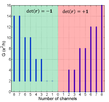
An alternative derivation of these ranges is presented in Appendix B. Apart from case discussed above, we see that topological case is also interesting as the conductance is uniquely determined by the topology, . Note that, in general for a topological SN junction these ranges imply . A simple situation in which this occurs is when the various transverse subbands are unmixed, with only one of them in the topological phase. Then the conductance is simply the sum of from the topological subband plus the contributions from all the non-topologicial subband. Without magnetic field or SOI, for small , and approximating the disordered junction as an ideal SN junction in series with a normal scattering region, the contribution from the non-topologicial subbands would be [NazarovBlanter, ]
| (15) |
where is the normal transmission probability through the junction for the non-topologicial subband. We expect this formula to remain true in the presence of spin orbit interaction and Zeeman field which have small characteristic energies compared to the Fermi energy and band width. We thus obtain
| (16) |
III Two Scattering Regions in Series
Another way of understanding the topological invariance of the determinant of the S-matrix in a system with disorder near the SN junction is to represent the disordered part of the normal wire by an -matrix, , as sketched in Fig. (2). This implies that is a unitary matrix allowing for incoming particles or holes from the left or right side in any of channels. relates incoming and outgoing waves to the left and right of the scattering region:
| (17) |
To be able to define this matrix, the normal wire has to be clean beyond a certain distance from the SN junction. Here and denote incoming and outgoing dimensional vectors of amplitudes from left/right side, respectively. The total reflection matrix is then obtained by combining the reflection matrix of the clean SN junction with . It would be natural to assume that only contains normal reflection and transmission amplitudes however, our proof continues to work even if also contains Andreev processes, provided that , which should be true provided there is no unpaired Majorana mode localized in the disordered part of the normal wire represented by . This can be seen especially in the opaque regime in which .
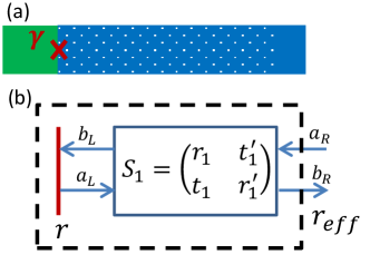
The effective reflection matrix for a disordered SN junction is obtained by combining this matrix with the reflection matrix of the clean SN junction, which satisfies . This equation can be used to eliminate and from Eq. (17) and show that the series system obeys with an effective reflection matrix (of dimension )
| (18) |
It can be easily seen that is unitary and particle-hole symmetric if and are. One way to see this is to use the Majorana representation of these matrices, Eq. (7) in which they are real and orthogonal, and show that defined by Eq. (18) is also real and orthogonal (see Appendix C). We now prove the important property
| (19) |
It is convenient to form a new matrix , out of the reflection matrix and the scattering matrix by
| (20) |
Obviously is orthogonal and we have . Next, we start with the identity
| (27) |
Here and represent corresponding diagonal matrices. Taking determinant of both sides we get
| (28) |
Here . Now we use the fact that is an orthogonal matrix and write
| (29) | |||||
| (30) |
Using the fact that has even dimension, we have . This together with Eq. (28) proves that which eventually proves the desired Eq. (19). Note that we did not make any assumption about the matrices except that they are orthogonal (unitary and obey particle-hole symmetry) and this derivation is valid for arbitrary . Thus we conclude that the additional scattering from disorder, corresponding to , does not change sign of the determinant of the reflection matrix. Whether the junction is topological (det ) or non-topological (det ) is unaffected by disorder [Brouwer11, , Wimmer11, ].
III.1 Treating contacts using series approach
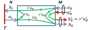
An interesting thing about our series approach is that Eq. (18) remains valid when the left and right sides have different number of channels, on the left side and on the right side as sketched in Fig. (3). To see this, note that the matrix can be a matrix, composed of matrix , matrix , matrix and matrix . is still unitary and and it obeys particle-hole symmetry . We can again write where is and after eliminating and , we see that and obey with matrix given above. Interestingly, even the determinant formula carries over to this case, i.e. .
Here, we would like to use these properties, to discuss a contact between the disordered nanowire with channels (coupled to the MM) and a 3 dimensional metal characterized by channels. After combining the reflection matrix of the disordered nanowire with the S-matrix of the ohmic contact we obtain a matrix . The question is what is the maximum conductance that this system can exhibit? Is it given by the number of channels in the quantum wire or in the 3D metal? See Fig. (3).
To answer this, we assume that the contact is far enough from the MM and the SN junction, (in a clean nanowire, the relevant characteristic length scales are Majorana screening cloud [AG2, ] and the coherence length of the superconductor ), that there are no Andreev processes taking place at the interface. Therefore, we can assume that the is block diagonal in electron and hole sectors, . Here is an matrix.
| (31) |
First, we look for solutions in which, an incoming is totally reflected and does not produce a . In other words
| (32) |
This contains equations for the unknowns and gives linearly independent incoming waves on the right side that are totally reflected and only channels, which are (partially) transmitted to the left side: .
Next we note that the fully reflected states, , are orthogonal both to the reflected part of the states, and also to the states transmitted from the left side, . This follows simply because
| (33) | |||
| (34) |
For the second equalities in both lines we have used unitarity of the matrix implying:
| (35) |
Thus we see that the fully reflecting states, , , completely decouple from the partially transmitting states, , , , . This implies that unitary transformations:
| (36) |
transform so that transforms to a propagating block and a reflected part . Therefore, we have
| (37) |
The horizontal/vertical line separate the first row/columns from the other rows/columns. , and are matrices and is an matrix.
Extending these unitary transformations to the hole sector by and applying them to in the particle-hole space we obtain
| (46) | |||||
| (70) |
where the lines separate the first components and the second components. The only off-diagonal elements in electron-hole basis come from . Defining and similar ones for , , and we can write the transformed in channel space as
| (71) |
where is block-diagonal in electron-hole space. An important feature of the conductance formula
| (72) |
is that for block-diagonal matrices, it is additive because only acts in the electron-hole subspace. In other words, we can write . is given by the first block of the matrix . The other contribution is composed of the second block of the matrix of which is totally diagonal in electron-hole space. Thus it commutes with , and since it is unitary, we get . Therefore, the conductance is completely determined by linear combination out of channels and . Thus for arbitrary disorder in the quantum wire and at the contact, the conductance bounds corresponding to channels apply, provided the conductance is sufficiently far from the junction.
IV Relativistic Field theory treatment
In order to understand the low energy conductance of this system, and, in particular, to include the effects of interactions in the normal portion of the wire [KAint, ], it is convenient [ACZ, ; Fidkowski12, ; AG, ] to write a low energy effective Hamiltonian, valid at energy scales , the induced superconducting gap. All degrees of freedom in the superconducting portion of the wire are integrated out in a Feynman path integral approach, leaving only the MM. The dispersion relations are linearized for the channels in the normal region. The effective Hamiltonian, written in the region only, is then a sum of the bulk term for the normal wire, a boundary term containing the tunnelling between the MM and the normal channels and including the effects of disorder near the junction:
| (73) |
Here , label left and right movers and a boundary condition is imposed, . labels the two spin split bands with different Fermi velocities, . is the MM operator, obeying , . represents an additional set of boundary interactions at , given by
| (74) |
where a sum over channel indices is implied in the first term and the matrix is Hermitian. Assuming that the disorder is extended over a finite length from the interface, at energies smaller than , it can be absorbed by the boundary interactions given above. These can be eliminated from the low energy Hamiltonian by a unitary transformation to the scattering basis (sec. IV.2).
IV.1 Channel-Resolved Conductance
Here we temporarily ignore . Despite the different Fermi velocities, this model actually has an symmetry before turning on the tunnelling terms, , upon defining rescaled fields so as to preserve the canonical anti-commutation relations:
| (75) |
where is an arbitrary velocity scale which drops out of physical quantities. It is then convenient to make an orthogonal transformation to a new basis of channels,
| (76) |
(where ) such that only couples to the MM. A single normal channel coupled to a MM is known to exhibit perfect Andreev reflection at zero energy [LawLeeNg09, , Flensberg10, ]. This is because the coupling to MM is infrared relevant in a renormalization group sense, so it grows at low energies and tends to enforce the boundary condition , the signature of pure Andreev reflection. Assuming that all the other channels are normally reflected, they do not contribute to the conductance. It then follows that, at zero energy, the channel-resolved linear conductances of the channels are
| (77) |
with total conductance, . Thus, a convenient way to determine the tunnelling parameters in the low energy effective Hamiltonian is by measuring the conductances for a given microscopic model. Although channel-resolved conductance is not topological, the easier-to-measure total conductance has some topological relevance as we saw above.
IV.2 Disorder and boundary interactions
Here we consider the effects of the additional boundary interactions of Eq. (74), which represent the effects of disorder near the SN interface in the low energy effective Hamiltonian approach. It is convenient to make an “unfolding transformation”, writing in terms of left-movers only on the infinite line, , by defining:
| (78) |
We then make the change of basis in Eq. (75) and finally, we go over to a basis of Majorana fermions defining:
| (79) |
where the matrix is defined in Eq. (8) and . The Hamiltonian then becomes:
| (80) |
where is a -dimensional real antisymmetric matrix, whose independent components are linear combinations of the real components of and , defined in Eq. (74). In this transformed basis, the solutions of the BdG equations have the simple form:
| (81) |
where and are 2-dimensional real vectors, related by the “reflection” matrix (more appropriately called a transmission matrix after unfolding):
| (82) |
Note that the physical spatial coordinates are obtained by , ensuring that the various components of the wave-function all have the same energy, . Next we observe that the boundary term in the Hamiltonian of Eq. (80) can be eliminated by redefining the Majorana fields by:
| (83) |
where is the step function. It then follows that the reflection matrix is
| (84) |
Since is real and anti-symmetric, is an SO(2N) matrix (with determinant ). A second SO(2N) rotation, by , puts in the form
| (85) |
The corresponding O(2N) reflection matrix, , is diagonal with entries and determinant -1. This corresponds to the perfect Andreev reflection in the first channel and perfect normal reflect in the other channel. Thus the total reflection matrix is:
| (86) |
Therefore ; the sign of the determinant of is unaffected by disorder.
V Conclusions
We have discussed the remarkable topological properties of SN junctions from two perspectives, one based on a series representation of the -matrix and one based on a low energy field theory approach. We have derived conductance bounds for a long quantum wire with an ohmic contact to a 3D metal, which depend only on the number of channels in the quantum wire (and the topological class of the junction) independent of any properties of the 3D metal.
Acknowledgements.
We than D. Pikulin for illuminating discussions and C. Beenakker for comments on an earlier verison of this manuscript. This research was supported in part by NSERC, CIfAR and the Swiss National Science Foundation.Appendix A BdG equation and S-matrix
A.1 Bogliubov-de Gennes equations
We begin by introducing a 4-component spinor of 3-dimensional fermion fields:
| (87) |
These obey
| (88) | |||||
| (89) |
where the indices , and we introduce 4 component Pauli matrices, which act on the particle-hole sectors
| (90) |
et cetera. and are zero and unit matrices. In terms of these operators, the second quanitized Hamiltonian of Eq. (1) can be written
| (91) |
where the Bogliubov-DeGennes (BdG) Hamiltonian is
| (92) |
Here and for are pauli matrices in spin and particle-hole bases, respectively and we have chosen real and positive for convenience, which can always be done by redefining the phases of the fermion fieids. Note that the single-particle Hamiltonian has the electron-hole symmetry
| (93) |
Without the term (negligible for narrow single-subband wires) the Hamiltonian is real, considering that , and has chiral symmetry (class BDI) but in general time-reversal symmetry and spin-symmetry is broken (class D). We assume that at , far from the SN junction on the normal side, the system can be regarded as clean so that a reflection matrix can be defined. The asymptotic scattering states can be decomposed into channels of particles and channels of holes. These channels in general mix spin components due to the spin-orbit interactions. can be odd or even depending on whether or not the Fermi energy lies in between the energy minima of two spin-split channels [KAint, ].
We introduce a -component spinor of fermion annihilation and creation operators corresponding to the channels:
| (94) |
The most general eigenfunction of energy has the form in the asymptotic region ()
| (95) |
The conserved quasi-particle current in the asymptotic region of large positive is:
| (96) |
where , is the Fermi velocity for electrons and holes in the channel. Since we consider , decays exponentially to zero for implying that the current, integrated across the cross-section of the quantum wire, obeys
| (97) |
Thus in Eq. (96) must be zero.
A.2 S-matrix
Defining component vectors:
| (98) |
the right-moving components of the asymptotic wave-function are linearly related to the left-moving components by the reflection matrix defined by . Requring Eq. (97) to be true for arbitrary incoming wave-function amplitudes, implies the conditions on the reflection matrix:
| (99) |
where we have defined the component vector:
| (100) |
It is convenient to define a unitary rescaled reflection matrix:
| (101) |
Appendix B An alternative proof of conductance range
We now sketch the details of an alternative proof of the bounds on the conductance for both topological and non-topological junctions and any number of channels, mentioned earlier in Eq. (14). It is convenient to define
| (104) |
so that Eq. (9) becomes:
| (105) |
To find the minima and maxima of the conductance, we can treat as a variational parameter and look for special matrices (and correspondingly matrices) for which has extremal values. Let be an matrix which gives the maximum or minimum conductance. Then must be stationary under a small variation
| (106) |
where is any real antisymmetric matrix. Noting that
| (107) |
we see that
| (108) |
Noting that , we see that is anti-symmetric. Therefore the trace of times this matrix cannot vanish for any anti-symmetric matrix unless
| (109) |
Noting that is purely imaginary, anti-symmetric and obeys , the most general possible commuting with has the form
| (110) |
Here the real matrix is anti-symmetric and the real matrix is symmetric with
| (111) |
Letting be the orthogonal matrix which diagonalizes the symmetric matrix , we can write:
| (112) |
where is diagonal, with entries which are the eigenvalues of and . Specializing to the case , we may use
| (113) |
where
| (114) |
The second of Eqs. (111) now implies that all matrix elements of the diagonal matrix must be . Furthermore, comparison of Eqs. (104) and (112)-(114) imply that
| (115) |
where each . On the other hand
| (116) |
Noting that all and that we find
| (117) |
We see that the maximum and minimum value of corresponds to all being and respectively, but whether or not this is possible depends on the sign of det . The maximum value of Tr with det is . The minimum value is or depending on the parity of and the sign of det . This then leads to Eq. (14), plotted in Fig. 1. We now show that allowing a non-zero matrix in Eq. (110) does not change this range. We again have the two conditions following from :
| (118) |
Since the square of an anti-symmetric matrix is negative definite, a non-zero , decreases the squares of the eigenvalues of ,
making it difficult to exceed the upper and lower bounds on found above assuming . Also note that a matrix
element can only be non-zero if . Thus at least two of the eigenvalues have opposite sign,
implying . Thus the bounds of Eq. (117) cannot be exceeded for either parity of nor either sign of .
So far we have considered a particular matrix which produces a given . We now prove that all orthogonal matrices giving the same have the same determinant (), completing the proof. Noting that
| (119) |
implies
| (120) |
where
| (121) |
We see that the needed result is equivalent to the statement that all orthogonal matrices, obeying Eq. (120), or equivalently
| (122) |
have determinant +1. Let . Consider the eigenvectors of a real matrix, , which commutes with . If is an eigenvector of with eigenvalue , then is an eigenvector of with eigenvalue . This implies that, in general, the eigenvalues of come in complex conjugate pairs, leading to det . The only possibility for an unpaired eigenvalue is real and also real. (If were real, and were not real, then would also be an eigenvector with the same eigenvalue.) In this case of a putative unpaired eigenvector, , since , it follows that is also an eigenvector of with the same real eigenvalue. Of course, since and are real, so is . But , so . Now suppose that . If this were true would have to be real since and are real. But then we have . This implies that , which is a contradiction. So we conclude that for any . Therefore is another eigenvector of , with the same eigenvalue , which is not proportional to . This contradicts the assumption that was an unpaired eigenvector. More explicitly, we can write the putative unpaired eigenvector as
| (123) |
where and are -dimensional vectors. Then
| (124) |
can only be proportional to if which contradicts the requirement that is real.
It can be seen that all values of within the ranges of Eq. (LABEL:Gb) can occur. This follows from observing that we can increase
from its minimum value in steps of by changing the sign of two of the ’s without changing the sign of det .
This change in sign of two of the ’s corresponds to an transformation which can be incorporated into .
A continuous set of transformations, with rotation angle varying from to , thus covers all values of in the interval of size .
Eq. (LABEL:Gb) is summarized in Fig. (1).
Appendix C Properties of the matrix
In this Appendix we show that the matrix defined in Eq. (18) is unitary and particle-hole symmetric if and matrices are. The particle-hole symmetry of follows from the fact that and each sub-matrix of separately obey particle-hole symmetry. Therefore,
| (125) |
Another way to see this would be to use the particle-hole symmetry of and to represent them as real orthogonal matrices. It follows from Eq. (126) that is also real. To establish its orthogonality, it is more convenient to analyse given by
| (126) |
where the right-hand contains elements of the real and orthogonal matrix defined in Eq. (20), obeying
| (127) |
Then we obtain
| (128) |
Using the fact that and the orthogonality conditions (127) we can write this expression as
| (129) |
where by we denote the expression
| (130) | |||||
| (131) | |||||
| (132) | |||||
| (133) |
Therefore, the right-hand side of Eq. (129) is equal to owing to orthogonality conditions (127) and .
References
- (1) A. Y. Kitaev, Phys. Usp. 44, 131 (2001).
- (2) Y. Oreg, G. Refael, F. von Oppen, Phys. Rev. Lett. 105, 177002 (2010).
- (3) R. M. Lutchyn, J. D. Sau, S. Das Sarma, Phys. Rev. Lett. 105, 077001 (2010).
- (4) J. Alicea, Rep. Prog. Phys. 75, 076501 (2012).
- (5) V. Mourik, K. Zuo, S. M. Frolov, S. R. Plissard, E. P. A. M. Bakkers, L. P. Kouwenhoven, Science 336, 1003 (2012).
- (6) A. Das, Y. Ronen, Y. Most, Y. Oreg, M. Heiblum, H. Shtrikman, Nature Phys. 8, 887 (2012).
- (7) M. T. Deng, C. L. Yu, G. Y. Huang, M. Larsson, P. Caroff, H. Q. Xu, Nano Lett. 12, 6414 (2012).
- (8) Turning off the pairing term in the superconducting region, there must be an odd number of active spin-split channels if the system is in the topological phase. However, by changing parameters such as the magnetic field at the junction it is possible to have an even number of active channels in the normal region. An example of this is discussed in [KAint, ], where mechanisms for abruptly changing the magnetic field are discussed.
- (9) Y. Komijani, I. Affleck, Phys. Rev. B 90, 107115 (2014).
- (10) A. Altland, M. R. Zirnbauer, Phys. Rev. B 55, 1142 (1997).
- (11) S. Ryu, A. Schnyder, A. Furusaki, and A. Ludwig, New J. Phys. 12, 065010 (2010).
- (12) C. W. J. Beenakker, J. P. Dahlhaus, M. Wimmer, A. R. Akhmerov, Phys. Rev. B 83, 085413 (2011).
- (13) M. Diez, J. P. Dahlhaus, M. Wimmer, and C. W. J. Beenakker, Phys. Rev. B 86, 094501 (2012).
- (14) C. W. J. Beenakker, e-print arXiv:1407.2131 (2014).
- (15) G. E. Blonder, M. Tinkham, T. M. Klapwijk, Phys. Rev. B 25, 4515 (1982).
- (16) D. .I. Pikulin, Y. V. Nazarov, Phys. Rev. B 87, 235421 (2013).
- (17) F. Merz, J. T. Chalker, Phys. Rev. B 65, 054425 (2002).
- (18) D. I. Pikulin, Y. V. Nazarov, JETP Lett. 94, 693 (2011).
- (19) I. C. Fulga, F. Hassler, A. R. Akhmerov, C. W. J. Beenakker, Phys. Rev. B 83, 155429 (2011).
- (20) A. R. Akhmerov, J. P. Dahlhaus, F. Hassler, M. Wimmer, C. W. J. Beenakker, Phys. Rev. Lett. 106, 057001 (2011).
- (21) I. C. Fulga, F. Hassler, A. R. Akhmerov, Phys. Rev. B 85, 165409 (2012).
- (22) B. Béri, Phys. Rev. B 79, 245315 (2009).
- (23) Y. V. Nazarov, Y. M. Blanter, Quantum Transport, Cambridge (2009).
- (24) P. W. Brouwer, M. Duckheim, A. Romito, F. von Oppen, Phys. Rev. B 84, 144526 (2011).
- (25) M. Wimmer, A. R. Akhmerov, J. P. Dahlhaus, C. W. J. Beenakker, New. J. of Phys. 13, 053016 (2011).
- (26) I. Affleck and D. Giuliano, Phy. Rev. B 90, 045133 (2014).
- (27) I. Affleck, J.-S. Caux, A. M. Zagoskin, Phys. Rev. B 62, 1433 (2000).
- (28) L. Fidkowski, J. Alicea, N. H. Lindner, R. M. Lutchyn, M. P. A. Fisher, Phys. Rev. B 85, 245121 (2012).
- (29) I. Affleck, D. Giuliano, J. Stat. Mech., P06011 (2013).
- (30) K. T. Law, P. A. Lee, T. K. Ng, Phys. Rev. Lett. 103, 237001 (2009).
- (31) K. Flensberg, Phys. Rev. B 82, 180516(R) (2010).