Strain-gradient-induced switching of nanoscale domains in free-standing ultrathin films
Abstract
We report first-principle atomistic simulations on the effect of local strain gradients on the nanoscale domain morphology of free-standing PbTiO3 ultrathin films. First, the ferroelectric properties of free films at the atomic level are reviewed. For the explored thicknesses (10 to 23 unit cells), we find flux-closure domain structures whose morphology is thickness dependent. A critical value of 20 unit cells is observed: thinner films show structures with 90∘ domain loops, whereas thicker ones develop, in addition, 180∘ domain walls, giving rise to structures of the Landau-Lifshitz type. When a local and compressive strain gradient at the top surface is imposed, the gradient is able to switch the polarization of the downward domains, but not to the opposite ones. The evolution of the domain pattern as a function of the strain gradient strength consequently depends on the film thickness. Our simulations indicate that in thinner films, first the domain loops migrate towards the strain-gradient region, and then the polarization in that zone is gradually switched. In thicker films, instead, the switching in the strain-gradient region is progressive, not involving domain-wall motion, which is attributed to less mobile domain walls. The ferroelectric switching is understood based on the knowledge of the local atomic properties, and the results confirm that mechanical flexoelectricity provides a means to control the nanodomain pattern in ferroelectric systems.
pacs:
77.55.-g.,77.80.bn,77.80.Dj,77.90.+kI Introduction
Flexoelectricity, the linear coupling between electric polarization and inhomogeneous deformation, is always allowed by symmetry in all insulators since strain gradients break inversion symmetry. This effect, found 50 years ago kog64 , has traditionally received little attention owing to its relatively weak effect in macroscopic samples. At the nanoscale, however, strain gradients are typically much larger than at macroscopic scales, as reduced dimensions imply larger gradients. The impressive progress in the design and control of nanoscale structures has motivated a revival interest in flexoelectricity, which has become an attractive topic in material science in the past few years zub13 ; yud13 ; lee12 . In the context of perovskite thin films, recent experimental breakthroughs leePRL11 ; gruv03 ; luSCI12 have revealed that the effect of strain gradients can be enormous in thin films, large enough to rotate or even switch ferroelectric domains. For instance, a recent experimental work luSCI12 , which in part motivated ours, shows that an inhomogeneous deformation caused by pressing the tip of an atomic force microscope over the surface of BaTiO3 films is able to switch the electric .
To model in a more realistic manner the flexoelectric switching in ultrathin ferroelectrics, it is important to include the domain morphology, which is expected to depend strongly on the mechanical and electrical boundary conditions yud13 . In the absence of electrodes or other sources of free charges that compensate the depolarizing field, it is well known that ferroelectrics respond by forming periodic arrays of domains, whose character might be described using the traditional models of Kittel (open flow) or Landau-Lifshitz (closed flow). For instance, ordered stripe domains of the Kittel type have been observed in PbTiO3 (PTO) films as thin as 3 unit cells deposited on SrTiO3 substrates, using x-ray photoelectron diffraction fong04 .
From the theoretical side, to understand and predict properties of nanoscale films at the atomistic level, there have been numerous studies using methods as well as simpler models constructed from them, such as model Hamiltonians and atomistic core-shell models. In particular, in PTO ultrathin films the ferroelectric and antiferrodistortive distortions in the (001) surface have been described mey02 ; bung05 ; sepli0506 , indicating also a decrease of tetragonality with stabilization of in-plane and antiferrodistortive reconstruction in the region near the surface. Studies of domain morphology reported vortex-like structures in films of a few unit cells thick lai07 ; behe08 . The changes in and lattice deformation across the and domain walls (DWs) hace also been investigated, with calculations performed in the material bulk mey02 ; shim08 and in films of 3-unit-cell thickness shim10 ; qu13 . However, none of these works describe the local properties of PTO ultrathin films and their correlation with the domain morphology as the thickness varies. Concerning this kind of simulations treating flexoelectricity, we can cite recent simulations involving a modified model Hamiltonian technique for (BaxSr1-x)TiO3 ponoPRB12 which has been used to calculate flexoelectric coefficients as a function of the film thickness and temperature, but without making any reference to the domain presence.
Then, although the flexoelectricity effect on nanoscale is attracting much attention, its exact role in the poling process of ultrathin films with a nanodomain configuration has not been completely characterized from the atomistic level. In this work, we address some particular questions, such as How does a local strain gradient affect the domain pattern in free-standing ultrathin films? and How does this depend on the film thickness and the strain gradient strength? To answer these, using a first-principles-based atomistic model we study the flexoelectric switching in ultrathin films of the stereotypical ferroelectric PTO, when a longitudinal strain gradient is applied locally over the center of one domain. Our simulations indicate that for the explored films, thinner than 10 nm, the domain patterns in the unstrained films are thickness dependent and responsible for the film being locally deformed. In agreement with this, the film response to a local and longitudinal strain gradient varies according to the nature of the domain pattern and as a function of the gradient intensity. The paper is organized as follows. Section II describes the computational details for modelling the film and the conditions for mimicking a strain gradient. Section III presents the results in two parts. First, the local properties of strain-free films are reported for two thicknesses in order to understand later the gradient-induced changes. Second, the domain pattern evolution for each of these films is investigated as the strain gradient strength is enhanced. Finally, the paper concludes with a summary in Sec.IV.
II Methodology: computational details
Prototype ferroelectric PTO is modeled using an atomistic core-shell model fitted completely to first-principles calculations (i.e., no explicit experimental data were used as input) as described in detail in ref. sepli04, . The model contains fourth-order core-shell couplings, long-range Coulombic interactions, and short-range interactions. It has shown to correctly reproduce the cubic-tetragonal phase transition in bulk sepli04 and also was able to describe the surface properties and interface effects of ultrathin films sepli0506 .
Here we study free-standing ultrathin films of PTO under ideal open-circuit electric boundary conditions performing classical molecular dynamics (MD) simulations using the DL-POLY package dlpoly at a constant temperature of 50 K, where PTO presents a tetragonal ferroelectric phase. Our films have two PbO-terminated surfaces and are modeled using supercells of unit cells. Periodic boundary conditions are applied along the in-plane pseudocubic [100] and [010] directions (axes and , respectively) but not along the [001] one (axis ) defined as the growth direction. The long-ranged electrostatic energy and forces are calculated by a direct sum method wolf which is a computationally efficient alternative to the Ewald summation. In the plane, the simulated supercell is kept constant and constrained to form a simple square lattice () of edge with =0.3866 nm, the in-plane lattice parameter in bulk computed at 50 K with the present model. The film thicknesses range from 4.0 nm (10) to 9.2 nm (23), where is the lattice parameter in the growth direction. Atoms are free to relax along all directions, except when mentioned, as long as they remain inside the simulation box.
Local polarization is defined here as the dipole moment per unit volume of a perovskite unit cell centered on the Ti ion and delimited by the eight Pb nearest neighbors at the corners of the box. We consider contributions from all atoms in the conventional cell and atomic positions with respect to that center:
| (1) |
where is the volume of the cell, and denote the charge and the position of the particle, respectively, and is a weight factor equal to the number of cells to which the particle belongs. The reference position corresponds to the core of the Ti atom, and the sum runs over 29 particles, including cores and shells of the surrounding ions (8 Pb and 6 O atoms) plus the shell of the Ti atom. Note that is independent of the origin for the vectors and vanishes when atoms are at their high-symmetry positions. The charge values are given in Ref. sepli04, .
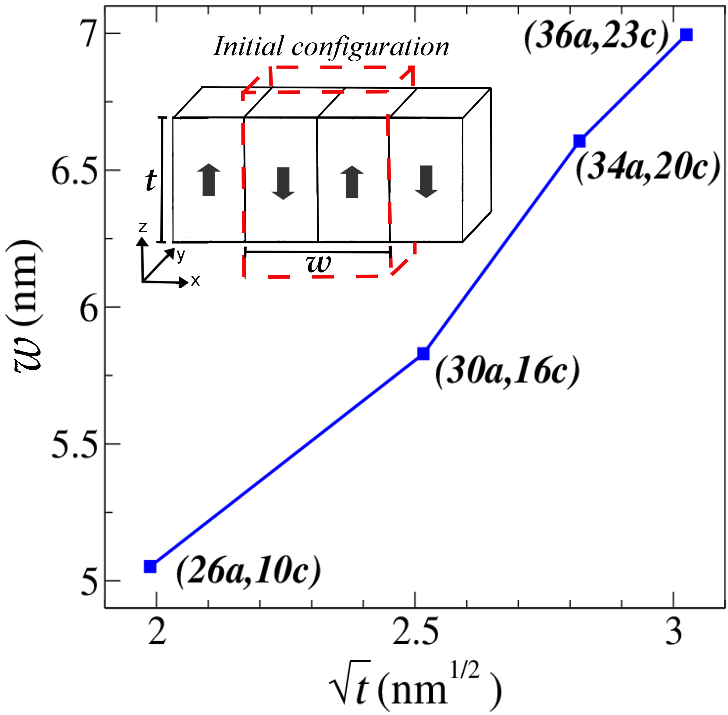
Inset: Schematic of the initial configuration of domains used to start the MD simulations for all the thicknesses. Supercell boundaries are indicated by dashed lines.
The initial configuration of the strain-free film for all the considered thicknesses is set up by creating 180∘ stripe domains with polarizations pointing upward and downward normal to the surface, alternated along the axis, as schematically shown in the inset of Fig. 1. The simulation supercell, indicated by dashed lines, holds only two domains. Based on previous results poy99 ; mey02 and also ours belle , which indicate that the 180∘ DWs centered at the Pb-O lattice planes are more stable than those at the Ti-O2 ones, we use the former in our starting configuration. Note that letting the structure relax will allow this domain configuration to change and the optimized one will depend on the film thickness as described below.
Strain gradient description. As we are interested in the effect of switching the out-of-plane polarization, we apply strain gradients in the direction normal to the surface, that is, a gradient of the out-of-plane strain component along the [001] direction denoted as . We impose a linear gradient localized on an in-plane square region of unit cells that penetrates until the central plane, which compresses the upper plane by a given strain and then decreases linearly in the intermediate planes until vanishing at the central cells. One advantage of using the present atomistic model to treat flexoelectric effects flex is that the interatomic potential does not need to be modified; it is sufficient to place the system under appropriate mechanical-boundary conditions that mimic the required gradient. To do that, one first has to establish the strain gradient in the film, noting that its presence implies a stress gradient which produces net forces acting on the atoms inside each unit cell. During MD simulations, the atoms will try to relax in order to vanish these net forces. Thus, in order to preserve the gradient a force pattern must be applied to the atoms in the unit cell; i.e., certain atoms must be fixed along the full simulation. Specifically, to set up the gradient, we start from the relaxed free film (which already presents a domain structure) and displace rigidly the atomic planes of the chosen unit cells until the average distance between consecutive Pb-O lattice planes equals the required local strains in order to have . We choose to freeze out the components of the Pb-core positions, allowing all other internal degrees of freedom (the Pb shell and other atoms, cores plus shells) to relax along all directions. Other choices are possible, for instance, the force pattern could be distributed between all atoms in the unit cell in different proportions DHV_11 . Finally, note that the local strain gradient induces an internal electric field which can compensate the depolarization field allowing that part of the free-standing film is poled.
III Results
III.1 Free-standing ultrathin films of PbTiO3
We focus first on strain-free films under ideal open circuit boundary conditions and revisit their local features. To begin with, the optimum lateral size of the simulation supercell (i.e., the number of cells ) is determined. For each considered thickness, we build up supercells of different lateral sizes, relax their structures, compare their total energies, and choose the lowest-energy one. The optimized structures are described below; here we just present the optimum width of one domain period as a function of the film thickness . Figure 1 displays the linear relation between and the root square of , showing the fulfillment of the Kittel law. We found that the optimum lateral sizes of the supercells are 26, 30, 34, and 36 for thickness of 10, 16, 20, and 23, respectively.
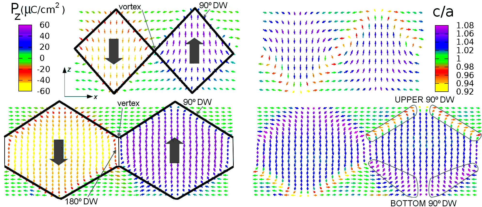
Hereafter we present results only for films of two thicknesses — 4.0 nm and 9.2 nm — because of their representative domain structures. Figure 2 shows a side view of cell-by-cell polarization map for the two thicknesses, where colors indicate the -component values in the left panels and the cell tetragonality in the right ones. Starting with the left panels, the 10 ultrathin film (top panel) shows a flux-closure arrangement around central cores or vortices. This vortex state, where the local orientation rotates continuously around one geometrical core, can also be described as a 90∘-domain loop. Indeed, we can demarcate upward and downward domains (hereafter UP and DOWN, respectively) with a rhombus shape surrounded by triangular caps (where is almost parallel to the surface) that complete an overall closed loop. Our simulations show that this domain morphology holds for thicker films until thicknesses of 20 unit cells. Above that critical value, the central vortices enlarge in the normal direction, giving rise to 180∘ DWs that grow together with the film thickness. Consequently, the shape of the UP and DOWN domains changes to hexagonal and a domain structure as envisioned by Landau-Lifshitz is formed, as shown in the bottom panels for a 23-thickness film. In this structure, in particular, we see that the 180∘ DWs end up in vertices or confluences of three DWs as predicted by Srolovitz and Scott scott86 and recently confirmed with high-resolution transmission electron microscopy images of Pb(Zr1-xTix)O3 jia11 .
As regards the thicknesses of the DWs, they vary depending on the type and location inside the film, the difference being more evident in the thicker films. In the inner region, the orientation of the changes abruptly from up to down over a distance of two lattice constants, creating very narrow 180∘ DWs, in agreement with previous theoretical results for defect-free walls mey02 . The 90∘ DWs instead differ according to their position with respect to the out-of-plane orientation, as indicated schematically in the bottom-right panel in Fig. 2 for the UP domain as an example, but the same behavior is repeated in the DOWN domain. In the top part, the rotates 90∘ in only three unit cells, leading to narrow 90∘ DWs. In the bottom part, instead, the rotates more continuously, requiring a few unit cells to change from the in-plane at the surface until pointing perpendicular, making these 90∘ DWs much broader. This behavior can be attributed to the electrostatic repulsion between the head-to-head wu06 ; gur11 in-plane s that confront each other at the junction of two triangular domains.
The cell-by-cell tetragonal ratio is indicated by colors in the right panels of Fig. 2, where and were obtained by taking the distances between pairs of nearest-neighbor Pb atoms along and , respectively. The cells inside the triangular domains with parallel to the surfaces are almost cubic, whereas those at the cores of the domains with perpendicular are tetragonal and their values are thickness dependent. Further, and in agreement with the high strain- interaction in PTO, these tetragonality maps demonstrate the difference between the 90∘ DWs. The narrow upper ones are well defined, presenting an abrupt change in the ratio as the tetragonal axis rotates from perpendicular to parallel to the surface; however, the broader ones at the bottom are characterized by a large tetragonality (reaching, for instance, 8% in the 23 film) which attenuates gradually in a few unit cells towards both sides. Concerning the 180∘ DWs in the thicker films, the tetragonality does not change notably, rather the wall is defined by an abrupt relative displacement or offset of the Pb atoms along . Finally, we emphasize the significant lattice deformation observed at the surfaces (shown by different colors in the right panels of Fig. 2) as well as across the film thickness specially in the 90∘ DWs.
To obtain further insights,
we monitor those properties in detail through the film thickness.
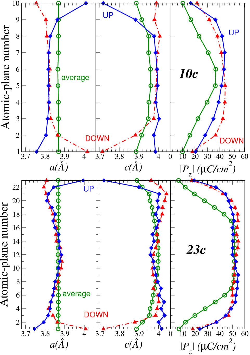
Figure 3 shows the in-plane and out-of-plane
lattice parameters across the thickness for both films.
Averaging these values over complete planes parallel to the surface [open (green) circles],
we find that the average local ’s remain constant across the film
due to the mechanical boundary conditions imposed on the simulation supercell.
The average values show the typical symmetric profile
determined by the two free surfaces: they are compressed at both surfaces
and gradually increase towards the inner film,
consistent with previous results sepli0506 .
However, examining closely at the central region of each domain,
the local ’s present an asymmetric distribution:
they are highly compressed in the two unit cells of the top surface
(with respect to the orientation)
and slightly enlarged at the bottom ones.
The strain change along [001] is compensated in the plane
only by the local lattice parameters , which behave oppositely to ,
but not by the parameters, which remain almost constants (not shown here),
corroborating that the unit cells at the surface neighborhood are
highly distorted.
This particular asymmetry through the thickness was also predicted
in superlattices of PTO/SrTiO3 from first-principles calculations junq12
and even in the limit case of PTO films of 1 thickness
whose unit cell is distorted qu13 .
Thus, this information together with the above description
shows that the free surfaces induce spontaneous strain gradients
that break the inversion symmetry in the film,
in agreement with previous works shim10 ; qu13 .
Furthermore, knowledge of the local strain maps
is essential to predict and understand the effect of
an imposed strain gradient.
Moving to the right panels of Fig. 3,
the profiles of the local modulus
show that the averaged values per lattice plane are symmetric.
Remarkably, inside each domain,
opposite to the highly asymmetric profiles of local ,
the profiles are almost symmetric
(in thinner films, actually they are slightly enhanced towards the top part).
Then we note that the modulus of and not follows the behavior across the film.
| Atomic layer | UP | DOWN | Triangular | Average | |
|---|---|---|---|---|---|
| 10 | 1 | 14.2 | 13.3 | 13.0 | 13.0 (11.4) |
| 2 | 1.0 | 2.9 | 3.5 | 2.8 (2.9) | |
| 3 | 6.0 | 6.2 | 6.4 | 6.5 (3.9) | |
| 4 | 4.9 | 5.1 | 5.2 | 4.9 | |
| 5 | 4.8 | 5.0 | 5.8 | 5.2 | |
| 23 | 1 | 14.3 | 13.0 | 13.0 | 13.1 (11.4) |
| 2 | 0.9 | 2.8 | 4.1 | 3.0 (2.9) | |
| 3 | 5.7 | 6.3 | 6.5 | 6.6 (3.9) | |
| 4 | 3.1 | 4.3 | 6.4 | 5.16 | |
| 5 | 3.0 | 4.1 | 6.1 | 5.1 | |
| 11 | 0.8 | 1.0 | 4.0 | 1.6 | |
| 1.0 | 1.0 | 3.9 | 1.0 (3.3) |
To end up this section, we analyze the local distribution of the antiferrodistortive distortion which has been shown bung05 ; step01 to coexist with the polar distortion at the surface, eventhough it essentially vanishes in bulk. It involves the oxygen octahedron rotation around the central Ti ion, where the rotation axis is the axis () with out-of-phase movements between neighbor cells on the (001) plane but successive in-phase movements along the [001]. Its strength is described by the rotation angle of TiO4 in the normal layer at each unit cell. Table 1 lists the rotation angle dependence of the atomic layers starting at the top surface, for the two films of interest and in different regions of the film by entering perpendicular to the surface: in the central cells of the UP and DOWN domain, and crossing the center of one triangular domain (reaching the central vortex of the 90∘ DW loop or the 180∘ DWs, depending on the film thickness). The last column reports the values averaged for each complete TiO2 atomic layer parallel to the surface. Moving along [001] in the center of one domain, it is found that the rotation angle of in the superficial cells decays towards the internal atomic layers: although it almost vanishes in the second layer, recovers in the third one, and then keeps decreasing slowly. It reaches the bulk value of 1o just at the eleventh layer of the 23 film, while in the thinner film, the superficial effects predominate. Furthermore, we note that cells in opposite surfaces differ in , which is also related to the different natures of the junction of the 90∘ DWs as explained before. On the other hand, when entering the film through the triangular domains, the distortions from the second layer towards the inner ones are a bit larger than those in the center of the UP and DOWN domains. Specifically, in the 180∘ DWs the distortion is about (the octahedra rotate to allow the abrupt change, in addition to the offset), versus the in the domain cores, where the cells are tetragonal with ferroelectric distortions mostly along . The averaged values show a behavior similar to that in the cores of the out-of-plane domain but with values 1o larger than in the inner cells due to the values in the DWs. Finally, note that our results for the first three atomic layers can be compared, and indeed fully agree with previous calculations reported using the present model sepli0506 as well as first-principles methods bung05 . Although those calculations have provided evidence of variation in the near-surface region, they were performed using smaller supercells than here and without any reference to the effect of the domain pattern. Hence, our inspection of the local distribution gives insights into the dependence of the domain morphology, especially in the DW neighborhood.
III.2 Film response to a local strain gradient
Now we investigate how the PTO film responds to a compressive strain gradient
applied locally as its intensity increases. We are particularly interested in following the
evolution of the domain configuration until eventually the polarization
switches in the strain-gradient zone. As the first step, we have to choose where
to apply the strain gradient.
Based on the observed local strain distribution in the central
region of each domain (Fig. 3), we suppose that
a compressive strain gradient on the top surface of the film
would only accentuate the already existent inhomogeneous compression
in the UP domain; on the contrary, it would alter the almost-constant
distribution in the DOWN domain. Therefore, we apply to the latter
a linear gradient on the top half of the film along the axis
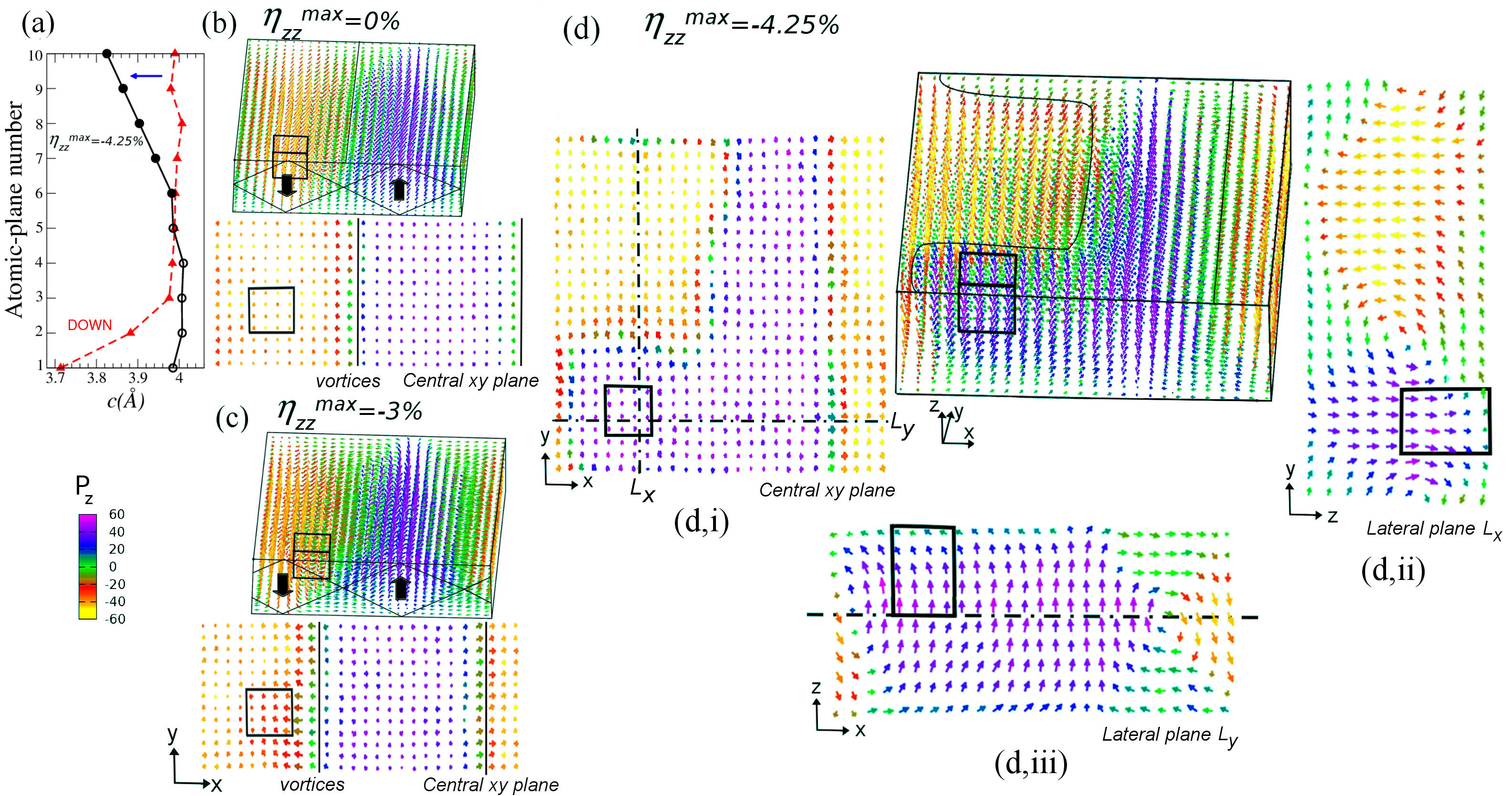
as described in Sec. II and shown in Fig. 4(a)
where the local profile is plotted before and after the application
for a particular of -4.25 %.
The same profile is established on a region of unit cells
that extends from the top surface to the central plane grad ,
as schematically indicated in the figure by a parallelepiped.
The strain gradient strength is increased progressively
by varying the compressive strain in the superficial cells
in intervals of -0.25 %.
For each strain gradient value, we carry out an MD simulations until the system
rearranges to that strain condition.
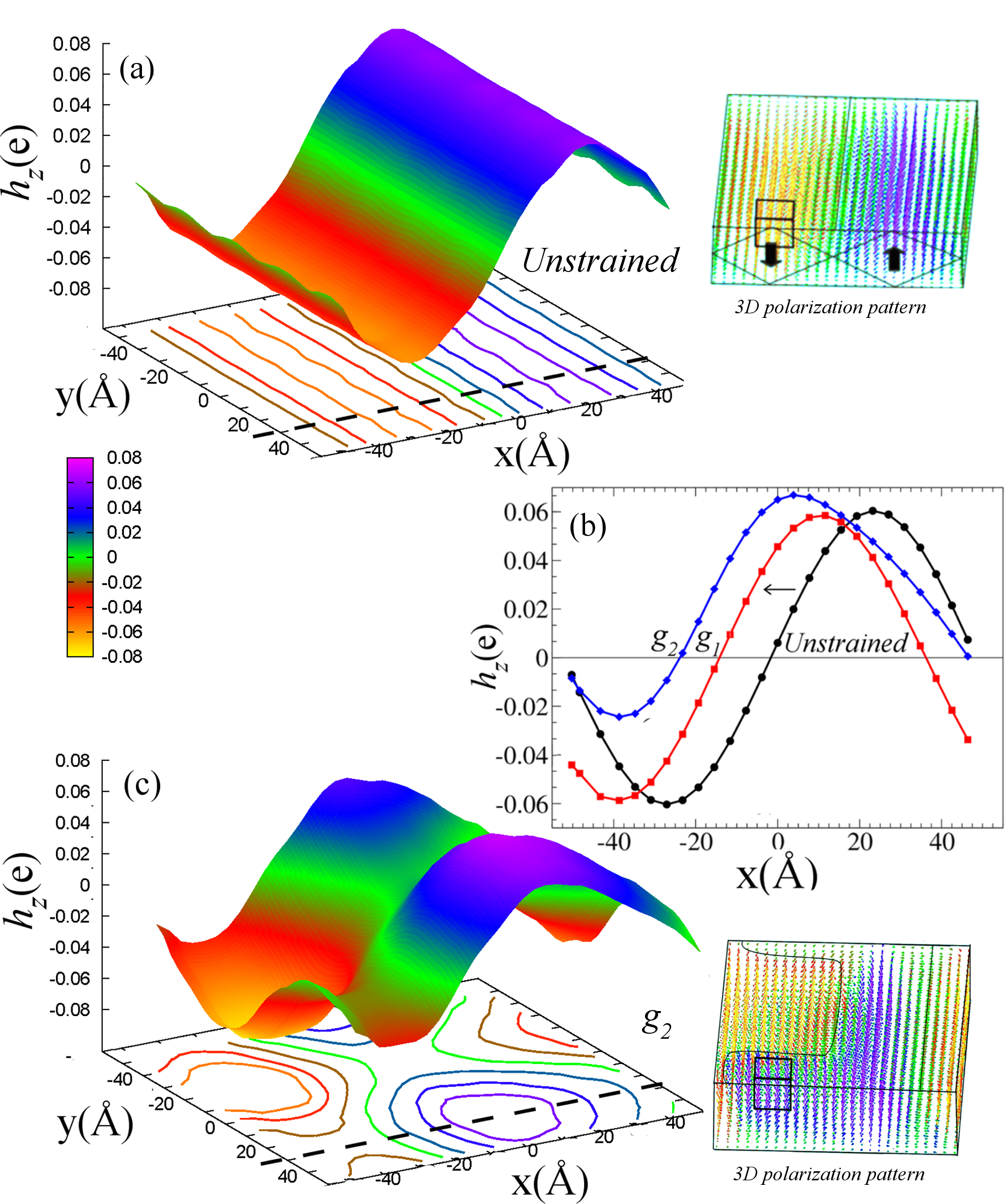
Thinner films. The results for the 10 film are illustrated in
Figs. 4(b)– 4(d) using three-dimensional (3D) maps of the local and
projections of them on different planes.
The unstrained film is shown in Fig. 4(b),
and how it changes when the imposed local strain gradient
takes two particular values,
namely, m-1 and m-1
in Figs. 4(c) and 4(d), respectively.
Starting with the unstrained film,
which is repeated here so as to have a reference
(same as the top panel of Fig. 2),
the 3D map displays a domain structure of 90∘ domain loops.
Its projection on the central plane shows only two domains
with the downward and upward perpendicular to the paper plane
separated by the central vortices,
whose positions aligned along the axis are indicated by a line in the figure.
The square in the DOWN domain identifies the region
where the strain gradient will be applied.
Thus, when the local strain gradient is imposed and as its strength
increases, we find that the response of the film
presents three different behaviors.
(I) For , no appreciable changes are observed
and the local distribution remains similar to that of the unstrained film.
(II) For , when , corresponding
to an of -3.00%,
the whole domain structure is displaced,
almost without changing either the size or the shape of the domains
as shown in the 3D map of Fig. 4(c).
The projection on the plane clearly shows that
the central vortices have been shifted in towards the gradient region
and sit just before its border.
distributions similar to this one are observed
as the gradient is further increased.
(III) For or -4.25%,
the dipoles rearrange and the local s in the gradient region,
initially downward, are switched
[3D map of Fig. 4(d)] inver .
This region has merged with the original UP domain,
extending its size and therefore changing its shape.
The new domain distribution can be appreciated more easily
in the projection on the central plane [Fig. 4(d,i)].
Also, we examine two lateral planes that cross the gradient region.
The projection on a plane shown in Fig. 4(d,ii)
(where all cells pointed downward before the gradient was applied)
reveals that the new domain pattern has developed a
flux-closure arrangement around the central vortices analogous to
that found in the unstrained film.
The projection on the plane [Fig. 4(d,iii)]
shows that most cells, including those in the gradient region, are poled upward.
The asymmetric distribution indicates that the
switching process has started in the vortices
that were brought close to the gradient region and now have disappeared,
while the other vortices remain on the right side.
Note that due to the supercell in-plane periodicity,
it is equally likely that in (II) the vortices had shifted in
towards the gradient region and therefore the switching process
would have started at the other side.
Further, we note that the profile in the gradient region, whose inferior part
[open circles in Fig. 4(a)] has been allowed to relax,
has adopted a profile quite similar to the one observed in the UP domains
of the unstrained films, as was assumed initially.
Finally, we want to remark that the observed movements of domains
in our free-standing films are allowed because of the absence of a substrate.
Its presence, however, can hamper the movement of domains,
as shown, for instance, in piezoelectric force microscopy images
of Pb(Zr0.2Ti0.8)O3 patterns in epitaxial thin films naga02 .
Hypertoroidal moment. In order to better describe the evolution of these complex dipolar configurations, we use the recently defined order parameter named hypertoroidal moment prosan07 , which provides a measure of subtle microscopic features. It involves the double cross product of the local dipoles with the vectors locating their positions,
| (2) |
where denotes the supercell volume, the subindex labels the transversal component, and the summation runs over all unit cells within the supercell. The transversal component can be approximated as , being the average of the individual dipoles over all the sites. This approximation is also valid for the expression in parenthesis. We refer the reader to Ref. prosan07, for a detailed discussion of this parameter. For 2D systems (i.e., systems periodic in two Cartesian directions and finite in the third one) such as the films considered here, once the simulation supercell is chosen, the value is independent of the origin used for . However, the magnitude and even the sign of do depend on the choice made for the supercell, leading to the multivaluedness of the parameter. We compute the hypertoroidal moment for different supercells whose centers scan the complete central plane of the original supercell. Therefore we explore for the first time a surface of and find that the changes in value and/or sign reflect modifications in the full distribution.
Although switching is a dynamical and complex process,
we may gain some insight by examining the surface of only
the -component of the hypertoroidal moment
(the other two Cartesian components are almost null)
as the imposed strain gradient increases.
Beginning with the unstrained film shown in Fig. 5(a),
we corroborate that the surface displays a sinusoidal dependence
along the direction with the same period
as the nanodomains and remains constant along the direction prosan07 .
Specifically, the maxima (minima) of extend along , coinciding
with the positions of the central cores of the UP (DOWN) domain,
while vanishes when rotation around the perpendicular axis exists,
certainly where the vortex centers sit.
Then as the strain-gradient intensity increases and following the distributions,
the response also presents three behaviors separated by
the gradient values and .
(I) For , the sinusoidal shape remains almost unchanged.
(II) For , when , in agreement with the distribution,
the surface shifts in as shows by
its projection on a transverse cut that crosses the central gradient region
[see the central curve in Fig. 5(b)].
behaves similarly as the gradient increases.
(III) For , needed to fully invert the in the
affected region, the surface shown in Fig. 5(c)
has changed dramatically, indicating that the 90∘-domain loop configuration
has been modified.
Two global extrema are observed, one maximum and one minimum, revealing that
the periodicity of the domain structure and thus the extended cores of the
each domain have vanished.
From the definition, we interpret that the minimum represents
the part of the DOWN domain farthest away from the gradient region
and therefore the less affected one,
whereas the maximum is located in the region of the UP domain farthest away
from the distribution of .
Fig. 5(b) shows that the profile in this particular direction
has slightly gained height in the positive branch, versus an important
reduction in the negative one,
reflecting the size enhancement of the UP domain at expenses of the DOWN domain.
Summarizing, the evolution of the hypertoroidal moment as a function of the strain
gradient strength provides information of the domain-structure evolution
localizing the domain cores and the vortices in a regular structure,
as well as their redistribution when the s in the strain region
are finally switched.
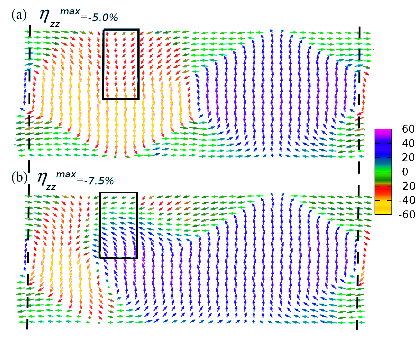
Thicker films. Figure 6 displays the -map projection on a transverse cut crossing the gradient region of a -thickness film for two strain-gradient values of m-1 and m-1, corresponding to of -5.00 and -7.50 %, respectively. As the gradient increases, starting at the surface the local s near and inside the gradient region rotate progressively until pointing parallel to the surface, i.e., their components decrease gradually [as shown in Fig. 6(a) for ] until they fully vanish. A lateral view in a plane, not shown here, indicates that the zone with parallel to the surface starts to grow and expands towards the bottom of the film as the gradient increases, then they are switched. For the value [Fig. 6(b)] the affected region is already poled upward and the asymmetric distribution shows that one of the 180∘ DWs is still immobile. Remarkably, as the gradient is increased further, the switched zone moves forward, generating vortices at the bottom as it continues growing laterally. Thus, unlike the DW movements observed in thinner films, we find that the DWs never move forward to the gradient region. This fact can be attributed to the relatively high energy barrier for the coherent motion of one entire DW compared to the DW case.mey02
In summary, we investigate from an atomistic point of view flexoelectricity-induced domain evolution. In free-standing PbTiO3 ultrathin films with thickness-dependent domain patters, we study the ferroelectric switching induced by a strain gradient acting locally in the direction normal to the surface. We first review the properties of strain-free films and confirm that the inhomogeneity of polarization, strain (strain gradient), and antiferrodistortive rotational angles appears not only among the surface cells but also in the neighborhood of the DWs. For the explored thicknesses (10 to 23 unit cells), we find flux-closure domain structures whose morphology is thickness dependent. A critical value of 20 unit cells is found: thinner films show structures with 90∘ domain loops, whereas thicker ones develop, in addition, DWs giving rise to structures of the Landau-Lifshitz type. When a compressive strain gradient normal to the surface acts locally at the top surface of the film, we find that it is able to reverse the normal polarization in DOWN domains but not in UP domains, which is understood based on the knowledge of the local strain distribution before imposition of the gradient. The evolution of the domain pattern as a function of the strain gradient strength depends, accordingly, on the film thickness. In thinner films, first one of the center of the DW loops moves towards the gradient region and then the affected region is gradually switched. In thicker films, instead, no DW movement is observed and the local polarizations in the gradient region are progressively reversed as the gradient strength is enhanced. This work contributes from an atomistic point of view to the understanding of the mechanical flexoelectricity in tuning domains in ultrathin films.
The authors acknowledge support from the Argentinian Agency ANPCyT through Grants PICT-PRH 99 and PICT-PRH 195. G.D.B. thanks to CONICET-Argentina for the Ph.D. fellowship.
References
- (1) S. M. Kogan, Sov. Phys. Solid State 5, 2069 (1964).
- (2) P. Zubko, G. Catalan, and A.K. Tagantsev, Annu. Rev. Mater. Res. 43, 387 (2013).
- (3) P. V Yudin and a K. Tagantsev, Nanotechnology 24, 432001 (2013).
- (4) D. Lee, and T. W. Noh, Phil. Trans. R. Soc. A 370, 4944 (2012).
- (5) D. Lee, A. Yoon, S. Y. Jang, J.-G. Yoon, J.-S. Chung, M. Kim, J. F. Scott, and T. W. Noh, Phys. Rev. Lett. 107, 057602 (2011).
- (6) A. Gruverman, B.J. Rodriguez, a. I. Kingon, R.J. Nemanich, J.S. Cross, and M. Tsukada, Appl. Phys. Lett. 82, 3071 (2003).
- (7) H. Lu, C.-W. Bark, D. Esque de los Ojos, J. Alcala, C. B. Eom, G. Catalan, A. Gruverman, Science 336, 59 (2012).
- (8) Fong, G.B. Stephenson, S.K. Streiffer, J. A. Eastman, O. Auciello, P. H. Fuoss, and C. Thompson, Science 304, 1650 (2004).
- (9) B. Meyer and D. Vanderbilt Phys. Rev. B 65, 104111 (2002)
- (10) C. Bungaro and K. M. Rabe, Phys. Rev. B 71, 035420 (2005).
- (11) M. Sepliarsky, M. G. Stachiotti, and R. L. Migoni, Phys. Rev. B 72, 014110 (2005), Phys. Rev. Lett. 96, 137603 (2006).
- (12) B.-K. Lai, I. Ponomareva, I. Kornev, L. Bellaiche, and G. J. Salamo, Appl. Phys. Lett. 91, 152909 (2007).
- (13) R.K. Behera, B.B. Hinojosa, S.B. Sinnott, A. Asthagiri, and S.R. Phillpot, J. Phys. Condens. Matter 20, 395004 (2008).
- (14) T. Shimada, K. Wakahara, Y. Umeno, and T. Kitamura, J. Phys. Condens. Matter 20, 325225 (2008).
- (15) T. Shimada, S. Tomoda, and T. Kitamura, Phys. Rev. B 81, 144116 (2010).
- (16) B. Yin and S. Qu, J. Appl. Phys. 114, 063703 (2013).
- (17) I. Ponomareva, A. K. Tagantsev, L. Bellaiche, Phys. Rev. B 85, 104101 (2012).
- (18) M. Sepliarsky, Z. Wu, A. Asthagiri, and R. E. Cohen, Ferroelectrics 301, 55 (2004).
- (19) W. Smith and T. R. Forester, computer code DL-POLY, Daresbury and Rutherford Appleton Laboratory, Daresbury, England.
- (20) D. Wolf, P. Keblinski, S. R. Phillpot, and J. Eggebrecht, J. Chem. Phys. 110, 8254 (1999).
- (21) S. Pöykkö and D.J. Chadi, Appl. Phys. Lett. 75, 2830 (1999); J. Phys. and Chem. of Solids 61, 291 (2000).
- (22) G. Belletti and S. Tinte, unpublished (2014).
- (23) We have checked that the present atomistic model for PTO is able to reproduce the longitudinal flexoelectric coefficient in the range of . belle
- (24) J. Hong and D. Vanderbilt, Phys. Rev. B 84, 180101 (2011).
- (25) D. J. Srolovitz, and J. F. Scott, Phys. Rev. B 34, 1815 (1986).
- (26) C.-L. Jia, K. W. Urban, M. Alexe, D. Hesse and I. Vrejoiu. Science 331, 1420 (2011).
- (27) X. Wu and D. Vanderbilt, Phys. Rev. B 73, 020103 (2006).
- (28) M. Y. Gureev, A. K. Tagantsev, and N. Setter, Phys. Rev. B 83, 184104 (2011).
- (29) Pablo Aguado-Puente and Javier Junquera, Phys. Rev. B 85, 184105 (2012).
- (30) A. Munkholm, S.K. Streiffer, M.V. Ramana Murty, J.A. Eastman, C. Thompson, O. Auciello, L. Thompson, J.F. Moore, and G.B. Stephenson, Phys. Rev. Lett. 88, 016101 (2001).
- (31) Two comments on the arbitrary size of the affected region: (i) that its deep depends on the film thickness indicates that, for the same compressive strain on the superficial unit cell, the gradient is weaker in thicker films; (ii) that the lateral size is kept constant means that the affected region is farther away from the 180∘ DW as the domain size increases together with the film thickness.
- (32) For a given value of strain gradient, the switching process ocurrs as a function of time during a molecular dynamics simulation, noting that the switching kinetics is beyond the scope of this work.
- (33) V. Nagarajan, A. Roytburd, A. Stanishevsky, S. Prasertchoung, T. Zhao, et al. Nat. Mater. 2, 43–4 (2002).
- (34) S. Prosandeev, L. Bellaiche, J. Mater. Sci. 44, 5235 (2009).