Electrical imprint effects on far infrared (FIR) transmittance spectrum in PZT ferroelectric films
Abstract
Tunable transmittance response in the THz range for a lead Zirconate Titanate Ferroelectric film under imprint effects and surface anisotropy is calculated by adapting the classical Landau Devonshire theory and the Rouard’s method. Induced electrical field is introduced by modulating the polarization profile, while the dielectric permittivity frequency dependence enters into the formalism by taking into the account the soft phonon mode E(TO1) contribution in the framework of the Drude-Lorentz model. It is found that two optical states of light transmittance emerge at zero applied field and normal incidence, and the intensities of transmitted light are closely correlated with the strength of imprint and the path of the electrical polarization.
Keywords: Multiferroics, Transmittance, Index of refraction.
DOI:http://dx.doi.org/10.1016/j.optcom.2015.02.011 PACS numbers:
I Introduction
Electrical imprint is generally considered as an undesirable effect in FeRAM technology mainly because it attempts against the data storage stability ben . Nevertheless, electrical imprint treatments on ferroelectric arrays have risen special interest in the last decade since they have demonstrated a crucial role in the design of the shape of non-volatile memories in piezoelectric actuators AKT . Physical origin of imprint is still under debate, although the ferroelectric degradation of polarization properties associated to non-switching surface layers with a large residual field in the electrode-ferroelectric frontier has been identified as one responsible mechanism for the shifting in the hysteresis loop Abe ,Zhou . Imprint control can be achieved either by exposing the sample during long periods and high temperatures Kadota , by manipulating the thickness of pinned domains on the free lateral surfaces Alexe or by injecting electronic charges into the electrode-ferroelectric interface via Schottky thermoionic current kr . First procedure has been successfully implemented in experimental lead zirconate titanate (PZT) optical shutters with stable performance on its dielectric susceptibility response after a long range of commutation pulses ()ohashi1 ,ohashi2 , outlining an alternate principle on light transmittance memory devices. Advances in the THz limit technology have also found promising proposals for low power operation on hybrid ferroelectric/graphene layer nanoplasmonic waveguides Gu ,Jin . On this scenario, we introduce the electrical imprint strength as an essential mechanism for the observed offset in the characteristic hysteresis loop, and calculate the effective index of refraction, the optical transmittance and the shape of memory under typical applied fields up to 300 kV/cm for 800 nm PZT systems in the edge of low THz. It is shown that asymmetric states of light transmittance arise by manipulating the strength of a vertical or horizontal imprint at zero field, in agreement with recent experimental reports ohashi2 .
II Transmittance Response Model
Figure (1) sketches the frame set for incident electromagnetic waves in the THz range interacting with a ferroelectric slab with variable index of refraction. Transmitted waves spectra are modified by imprinted and externally electrical field .
The classical Landau-Ginzburg-Devonshire (LGD) model modelLGD ,FD ,Chandra provides the description for the polarization field distribution in ferroelectric (FE) phase under an applied electrical field . The single component for the polarization field is obtained by solving the third order non-linear differential equation:
| (1) |
where and are the typical parameters taken from the renormalized Gibbs free energy functional in the -phase configuration Khare , corresponds to the correlation length in FE state and defines the relative (and uniform) field intensity along -direction. The polarization field distribution profile nearby the surface of a ferroelectric film of thickness changes with its perpendicular distance as
| (2) |
according with the Kretschmer’s theory K . encodes the asymmetric depolarization field effects due to a large variety of phenomena, among others, the relative orientation of respect to the normal of the surfaces, the proximity vacuum-interface boundary depletion field or the mismatch strain for samples in contact with a substrate Wang . In the frame of a linearized approach, the complete polarization profile is constructed by writing , where is taken as the average polarization of the film calculated from (1), and corresponds to the spatial fluctuations around . Therefore, must satisfy:
| (3) |
with . The solution for with boundary conditions (2) is given explicitly by:
| (4) |
where , and the structure factor takes into account the characteristic lengths in the system, namely, the thickness , the surface depletion and the renormalized coherence length in the FE state , which depends on the transition temperature and the external field intensity. The dependence for the average polarization must be obtained self-consistently Lu . Factor is calculated as . By inserting the adjustment correlations in terms of the coercive field and the remnant polarization at zero field as and , the expression for the dielectric susceptibility as an intrinsic function of applied field in the framework of the Landau-Khalatnikov theory is derived coercive ,LK :
| (5) |
with . Hence, the inhomogeneous index of refraction is written as eliseev ,Vivas :
| (6) |
with . The correlation with the phase difference associated to the optical path traveled by a coherent electromagnetic wave for those spatially inhomogeneous systems is calculated through the definition phased :
| (7) |
where is taken as the effective value for the index of the refraction in the length :
| (8) |
represents the incomplete elliptic integral of the second kind elli with and . Far infrared dielectric response of Lead (Zirconate) Titanate (PT-PZT) have been intensively investigated by using the classical Drude-Lorentz type model in the THz range Fedo ,Buix ,Nakada :
| (9) |
where THz and correspond to the adjusted frequency of the phononic E(TO1) soft central mode selected for (undoped) PZT films Li ,Wangg . Its relationship with the factor in Equation (8) is given by . Two Debye relaxation mechanisms are present in the permittivity response model, however, they lie into the GHz range and do not have significant effects on the transmittance spectrum in the interval of interest. The transmittance response is calculated by using the Rouard’s method for normal incidence as a function of the phase difference , the film index and its environment Lecaruyer ,Heavens :
| (10) |
and . Equations (7)-(10) constitute the core results in this paper: the transmittance spectrum due to the propagation of electromagnetic (THz) radiation in a ferroelectric film under vertical and horizontal imprint effects. Numerical results are discussed in the next section.
III Results
Electrical polarization induced by imprint treatment has been qualitatively set into the formalism in terms of the saturation and coercive fields under the adjustment in Eq. (5), with Tag ,Grossmann ,NI . Parameter might encode the relative vertical imprint strength, and its negative value indicates that imprinting treatment has been performed by inducing an external polarization field in opposite direction relative to . Factor represents the horizontal shift taken as a fraction of the coercive electrical field . Figure (2) compares the hysteresis profile for a symmetrical loop without imprint treatment (black line), its vertical shifting under imprint effects for (red line) and the characteristic bias for (blue line). Five regimes are readily identified depending on the sign in : () direct polarization for positive increasing field, () saturation at , () depolarization, () reverse saturation at and () direct polarization for negative increasing field.
Numerical simulations for the hysteresis loop and dielectric susceptibility were performed for PZT films with approximated parameters reported in reference ZZ . Figure (3) (a) depicts the relation at THz and . When non-imprinting procedure is taken into account, the hysteresis loop remains symmetrical around axis, and the bi-state optical transmittance mode vanishes (single black dot in line (a) at ). The spectrum exhibits a symmetrical butterfly shape with minimal transmittance peaks at the coercive fields . In the case (curve (b)), the spectrum is horizontally biased and two states of light transmittance emerge at zero field depending on the path of the polarizability () or (). The minima of remain symmetrical around its crossing point (identified as the electrical field value for which the transmittance function gets the same value for direct and inverse polarization), with higher values compared with the case (a). Line (c) is calculated for and . The crossing point is shifted for negative values of the externally applied field, the butterfly-shape symmetry breaches and the spectrum shows its maximum difference for the transmittance levels at , indicating that a stronger optical response arises when the vertical imprint treatment predominates.
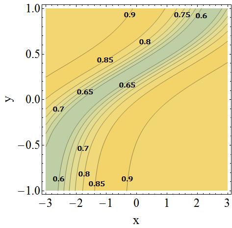
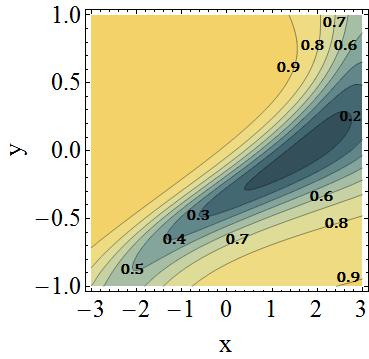
Figure (4) shows the evolution of the transmittance spectrum at fixed frequency (0.1 THz) for independent values of and in the range between and respectively, with the largest difference around 75 (labeled in open circles) at . Figure (5) illustrates the transmittance for different imprint strengths from up to 25 THz in the far infrared edge (FIR) for direct and inverse polarization. Absorption associated to the E(TO1) phonon mode becomes apparent under vertical imprint for THz (line c) and is essentially absent for horizontal bias. In the range of higher frequencies (>10 THz), the film exhibits peaks of transparency whose positions depend on the values of and . The transmittance overlaps their lines regardless its polarization bias for (curve a), but it takes two values depending on the cycle history when imprint effects are included into the calculations. Figures (6) and (7) show the contour lines in the transmittance response for simultaneous imprint strengths in two different paths of polarization. On the process the response changes monotonously from 0.65 to 0.9 in contrast with remarkable variations after calculating it upon the trajectory. Optical transmittance differences at zero field for direct and inverse polarization states as a function of the positive imprint strengths and various frequencies in the THz regime are shown in Figure (8). Non shape memory effect is available without imprinting treatment (). response is sensitive to the external radiation frequency since it tends to increase as the frequency approaches to the edge of the far infrared regime ( THz). The E(TO1) phonon mode contribution becomes significant in the range between 1 to 3 THz, as referred in the -crossover.
Figures (9) and (10) describe the shape of the memory as a function of the external frequency for horizontal and vertical imprinting shift, respectively. The maximum of lies at (line c′ in Fig. (9)) and (line b in Fig. (10)) for frequencies below 0.1 THz, as already demonstrated in Figure (4). The effective index of refraction is modified by imprint procedures and phononic excitations for higher frequencies, affecting the transmittance functionality by diminishing its response as long as the frequency reaches the 5 THz limit.
IV Conclusions
The explicit relationships for the effective index of refraction and the transmittance response in ferroelectric (PZT) films with surface anisotropy and induced electrical imprint are calculated by recasting the LGD model and Rouard’s technique. It is shown that the transmittance spectrum is highly sensible under imprint strength in the edge of Terahertz range (0.1-1 THz) and depolarizing regime for 800 nm samples. Our approach is solely focused on the vertical and horizontal hysteresis loop displacement, although the model might be directly extended for asymmetrical slanted loops, resembling recent experiments reported for PZT films under Ba+2 (Sr+2) modifications of dopant concentration in Pb sites Ng , broadening a wide set of possibilities in electrochemical control on remnant polarization, coercive field and piezoelectric response in these ceramic materials. in equation (4) might be solved exactly, the line becomes slightly different compared with the proposed hyperbolic profile, but this procedure does not change in significant way the main behavior on the transmittance response. Detailed studies on the role of Zr/Ti compositional variation in PZT films have also demonstrate a close correlation between critical temperature , the short-long structural order crossover passing through rhombohedral-morphotropic phase boundary (MPB)-tetragonal phases, and piezoelectric activity in Lead Titanate system Jaffe ,Noheda ,Glazer ,DJF , recalling the pertinence of LGD model for transitional states, specifically in its characteristic length . Transmittance measurements in ferroelectric thin film structures allow to perform indirect adjustments to Drude-Lorentz model (9) on its soft mode and damping parameters as the dielectric permittivity changes up to 10% for kV/cm Kuzel1 and 65% and 67 kV/cm for strained samples Kuzel2 . Long-lasting imprint exposure in ferroelectric films, their intrinsic loss of polarization and retention effects might acquire relevance in highly confined systems with nm, and they constitute interesting issues that shall be considered on further investigations.
V Acknowledgements
The author acknowledges availability and technical support at CER Computer Lab.
References
- (1) J. M. Benedetto, Integrated Ferroelectrics: An International Journal 15 (1997) 29.
- (2) A. Gruverman, B. J. Rodríguez, A. I. Kingon and R. J. Nemanich, A. K. Tagantsev, J. S. Cross and M. Tsukada, Applied Physics Letters 83 (2003) 728.
- (3) K. Abe, N. Yanase, T. Yasumoto and T. Kawakubo, Jpn. J. Appl. Phys. 41 (2002) 6065.
- (4) Y. Zhou, H. K. Chan, C. H. Lam and F. G. Shin, Journal of Applied Physics 98 (2005) 024111.
- (5) Y. Kadota, H. Hosaka and T. Morita, Ferroelectrics, 308 (2008) 185.
- (6) M. Alexe, C. Harnagea, D. Hesse and U. Gösele, Applied Physics Letters 79 (2001) 242 .
- (7) W. Y. Kim, Y. S. Lee, H. C. Lee, D. Y. Ka and S. Y. Kim, Journal of the Korean Physical Soc., 57 (2010) 1690.
- (8) T. Ohashi, H. Osaka and T. Morita, Japanese Journal of Applied Physics, 47 (2008) 3985.
- (9) T. Ohashi, H. Osaka and T. Morita, Applied Physics Letters, 93 (2008) 192102 .
- (10) X.-Q Gu, W.-Y. Yin, Optics Communications, 319 (2014) 70.
- (11) D. Jin, A. Kumar, K. H. Fung, J. Xu and N. X. Fang, Applied Physics Letters, 102 (2013) 201118.
- (12) A. K. Tagantsev, V. O. Sherman, K.F. Astafiev, J. Venkatesh and N. Setter, J. Electroceram. 11 (2003) 5.
- (13) V. Fridkin and S. Ducharme, Ferroelectricity at the Nanoscale, NanoScience and Technology, Springer-Verlag (2014) DOI: 10.1007/978-3-642-41007-9_1.
- (14) P. Chandra, P. B. Littlewood, cond-mat/0609347.
- (15) P. Khare and D. Sa, Solid State Communications, 152 (2012) 1572.
- (16) R. Kretschmer and K. Binder, Physical Review B, 20 (1979) 1065.
- (17) C. L. Wang et-al., Solid State Communications, 109 (1999) 213.
- (18) T. Lü and W. Cao, Microelectronic Engineering, 66 (2003) 818.
- (19) S. Kim and V. Gopalan, Applied Physics Letters 80 (2002) 2740.
- (20) P. Chandra, P. B. Littlewood, Physics of Ferroelectrics, Topics in Applied Physics, 105 (2007) 69.
- (21) E. A. Eliseev, A. N. Morozovska, J. Mater. Sci. 44 (2009) 5149.
- (22) H. Vivas C. and C. Vargas-Hernández, Physica B 12 (2012) 2089.
- (23) Lakshminarayanan V. et al., Lagrangian Optics, Springer Netherlands, (2011).
- (24) http://functions.wolfram.com/08.04.02.0001.01, .
- (25) I. Fedorov, J. Petzelt, V. elezný, G. A. Komandin, A. A. Volkov, K. Brooks, Y. Huang and N. Setter, J. Phys.: Condens. Matter 7 (1995) 4313.
- (26) E. Buixaderas, S. Kamba and J. Petzelt, Ferroelectrics, 308 (2004) 192.
- (27) M. Nakada, K. Ohashi and J. Akedo, Japanese Journal of Applied Physics, Vol. 44 (2005) 6918.
- (28) E. Buixaderas, et-al Phase Transitions: A Multinational Journal, 83 (2010) 917.
- (29) D. Wang, J. Weerasinghe, A. Albarakati and L. Bellaiche, Int. J. Mod. Phys. B 27 (2013) 1330016.
- (30) P. Lecaruyer, E. Maillart, M. Canva and J. Rolland, Applied Optics 45 (2006) 8419.
- (31) O. S. Heavens, Optical Properties of Thin Solid Films, Chapter 4, Dover Publications (1991).
- (32) A. K. Tagantsev, I. Stolichnov, N. Setter and J. S. Cross, Journal of Applied Physics 96 (2004) 6616.
- (33) M. Grossmann, O. Lohse, D. Bolten, U. Boettger, R. Waser and T. Schneller, Journal of Applied Physics 92 (2002) 2680.
- (34) N. Inoue and Y. Hayashi, IEEE Trans. Electron. Devices, 48 (2001) 2266.
- (35) Z. Bi, Z. Zhang and P. Fan, Journal of Physics: Conference Series 61 (2007) 120.
- (36) M. D. Nguyen et-al, Ceramics International 40 (2014) 1013.
- (37) B. Jaffe, W. R. Cook and H. Jaffe, Piezoelectric Ceramics (Academic, London, 1971), p. 131.
- (38) B. Noheda, D. E. Cox, G. Shirane, J. A. Gonzalo, L.E. Cross and S-E. Park, Applied Physics Letters, 74 (1999) 2059.
- (39) A. M. Glazer, P. A. Thomas, K. Z. Baba-Kishi, G.K.H. Pang and C. W. Tai, Physical Review B 70 (2004) 184123.
- (40) D. J. Franzbach et-al, Sci. Technol. Adv. Mater. 15 (2014) 015010.
- (41) P. Kuel, F. Kadlec, H. Nmec, R. Ott, E. Hollmann and N. Klein, Applied Physics Letters 88 (2006) 102901.
- (42) P. Kuel, F. Kadlec, J. Petzelt, J. Schubert and G. Panaitov, Applied Physics Letters 91 (2007) 232911.