First-Principles Approach for Energy Level Alignment at Aqueous Semiconductor Interfaces
Abstract
A first-principles approach is demonstrated to calculate the relationship between aqueous semiconductor interface structure and energy level alignment. The physical interface structure is sampled using density functional theory based molecular dynamics, yielding the interface electrostatic dipole. The approach is used to place the electronic band edge energies of the semiconductor relative to the occupied energy level in water. Application to the specific cases of non-polar facets of GaN and ZnO reveals a significant role for the structural motifs at the interface, including the degree of interface water dissociation and the dynamical fluctuations in the interface Zn-O and O-H bond orientations. These effects contribute up to 0.5 eV.
The alignment of electronic energy levels at a heterointerface between two materials represents both a fundamental materials interface characteristic and a crucial property that controls electronic device functionality in such diverse areas as semiconductor electronics, batteries and electrochemical cells. In the case of semiconductor interfaces, the energy level alignment is encapsulated in the valence band edge energy offset, and a hierarchy of theoretical approaches to calculate it have been established Franciosi and Van de Walle (1996). However, the corresponding energy level alignment at solid-electrolyte interfaces poses a substantially more complex problem. In particular, development of a constructive, first-principles theory for the alignment of semiconductor band-edge potentials to electrochemical potentials still presents fundamental challenges Cheng and Sprik (2012).
As a significant example, the relative alignment of the semiconductor band edge and the corresponding redox level in the solvent for a target reaction determines thermodynamically whether photoexcited carriers in the semiconductor can drive the reaction and with what range of overpotential. This is of fundamental importance in the design of electrochemical devices for solar energy harvesting Nozik and Memming (1996); Kudo and Miseki (2009). In particular, it is an unavoidable constraint in the search for materials that can serve both as efficient absorbers of the solar spectrum and to supply electrons and holes with sufficient energy to drive relevant reactions, e.g., the hydrogen evolution reaction or the water oxidation reaction.
In practical electrochemical measurements, the interface presents a complex system: a doped semiconductor, an aqueous interface of generally unknown atomic structure that may well participate in acid-base reactions and the water with dissolved ions and a particular . Through control of the applied bias and the , conditions corresponding to both flat bands in the semiconductor and zero zeta potential in the water can be achieved. The latter refers to the condition of zero net interface charge due to acid-base activity at the interface (adsorption of and ) Cheng and Sprik (2012). Under these conditions, the interface specific alignment of the semiconductor band edges to the scale of redox levels in water can be measured. In turn, this alignment determines semiconductor band bending and water double-layer formation under general conditions of doping, ion concentration, bias and .
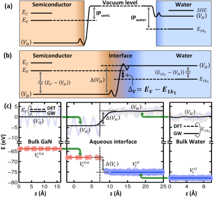
In order to circumvent the complexity of these interfaces and seek trends across semiconductors, a simplified picture is appealing Butler and Ginley (1978). Imagine opening up the interface so that one can characterize a reference semiconductor surface and a water surface separately (Fig. 1a). On the water side, the position of the highest occupied states of bulk water () are known from photoemission measurements Winter et al. (2004). The redox level defines the standard hydrogen electrode (SHE) and its absolute value relative to vacuum has been established Cheng and Sprik (2012); Trasatti (1986). On the semiconductor side, the ionization potential and electron affinity fix the band edge positions relative to the vacuum. Taken together, a model of the energy level alignment emerges. What additional physical effects at the real interface alter this simple picture and how large are they?
In order to probe the impact of realistic semiconductor-water interface structure, a constructive theory for the energy level alignment is required. While distinct approaches have been explored Cheng and Sprik (2012, 2010); Wu et al. (2011); Cheng and Selloni (2010), at a key point in the analysis Kohn-Sham energy eigenvalues from Density Functional Theory (DFT) are used to approximate electronic excitation energies. This is well known to fail formally and practically, e.g., the well-known band gap problem Jones and Gunnarsson (1989). The approach in many-body perturbation theory offers a well-founded theory for excitation energies Hybertsen and Louie (1986); Godby et al. (1987); Aulbur et al. (2000). Recent applications of the approach to liquid water demonstrate substantial corrections for key electronic levels Swartz and Wu (2013); Pham et al. (2014). For trends in electrochemical energy level alignment, based on the simplified model in Fig. 1a, recent studies have incorporated corrections from the approach Toroker et al. (2011); Li et al. (2013); Stevanovic et al. (2014). The broadest survey considered the calculated band edges, the available photoemission data for the semiconductor surfaces, and electrochemical data Stevanovic et al. (2014). The authors infer that semiconductor-water interface structure contributes about 0.5 eV to the alignment, albeit without explicit treatment of such structure.
Here we demonstrate a first-principles approach to calculate the electronic excitation energy level alignment at specific semiconductor-water interfaces (, Fig. 1b). To do so, we must integrate dynamical sampling of the physical and electronic structure of both water and the aqueous interface with the approach for the excitation energies.
Our approach builds on the established methodology used for semiconductor interfaces Van de Walle and Martin (1986); Zhang et al. (1988); Hybertsen (1991); Franciosi and Van de Walle (1996); Shaltaf et al. (2008). DFT is utilized for the microscopic charge distribution at the interface, responsible for the interface-specific intrinsic dipole, while the approach is used for the calculation of the excitation energies in the semiconductor and in the water. Three separate calculations are required: one each for the bulk materials and a third for the interface properties. The final energy level alignment combines the results from these three calculations as illustrated in Fig. 1c, where the suitably averaged electrostatic potential () or core potential is used for reference.
To represent the properties of the solid-liquid interface, ab initio molecular dynamics (MD) are used to simulate ambient conditions. Electronic properties are determined by averaging a sample of configurations to represent the thermal average and include the impact of finite temperature renormalization of the energy levels, albeit in a semiclassical approximation Lax (1952); Cardona and Thewalt (2005). Our theory provides the semiconductor valence band alignment to the centroid of the band in liquid water
| (1) | |||||
This result links to the electrochemical scales in water and the vacuum scale through the .

We demonstrate our approach for the specific cases of GaN and ZnO interfaces with water, motivated by the utility of GaN/ZnO mixed crystals for photocatalysis with visible light Maeda et al. (2006) and the recent observation that the facet dominates the activity for GaN nanowires Wang et al. (2011a). We have recently analyzed the atomic-scale structure at these aqueous semiconductor interfaces using DFT-based MD simulations, demonstrating the role of interface water dissociation Kharche et al. (2014). The same technical protocol is used here Blöchl (1994); Kresse and Furthmuller (1996); Kresse and Joubert (1999); Jensen et al. (2008); Dion et al. (2004); Klimes et al. (2011); Lan , including use of the projector augmented wave (PAW) method Blöchl (1994) as implemented in VASP Kresse and Furthmuller (1996); Kresse and Joubert (1999), with the functional optB88-vdW Dion et al. (2004); Klimes et al. (2011) that includes long-range van der Waals interactions. See the Supplemental Material for details Sup .
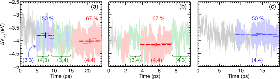
A snapshot of the equilibrated structure for the GaN case (Fig. 2a) shows that water near the interface with GaN spontaneously dissociates resulting in a fully hydroxylated surface, in agreement with prior work Shen et al. (2010); Wang et al. (2011b); Kharche et al. (2014). All surface N sites are protonated while all surface Ga sites are bonded to the corresponding ions. The average density of water, the characteristics of the hydrogen bonds, the valence band density of states (DOS, not shown) and the O-O pair distribution function (excluding the near-surface regions) are close to those calculated for bulk water (Fig. 2b-d) and experiment Soper and Benmore (2008). For the ZnO interface, the interface water layer is partially dissociated. Half of the adsorbed water molecules dissociate for a interface cell, in agreement with earlier studies Dulub et al. (2005); Tocci and Michaelides (2014); Kharche et al. (2014). For a cell, in-plane boundary conditions result in fluctuations in the fraction of water dissociated at the interface, including intervals where it is 67%, providing another structure for study.
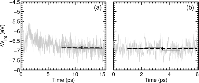
To extract the average potential step between the semiconducting region and the water region, the electrostatic potential profile is calculated for 50 snapshots sampled from a 5 ps window. These are averaged laterally to obtain the traces shown in Fig. 1c, followed by a running average and a time average. The resulting average electrostatic potential is flat both in the center of the semiconducting region and in the center of the water region; interface effects are localized. In practice, the PAW core potential, illustrated in Fig. 1c, provides an accurate, physically equivalent approach. It is readily available for every MD snapshot and averages are performed using all snapshots in the chosen time window. Comparison of averages over a series of shorter time windows (1-2 ps each), suggests an error bar of less than 0.1 eV due to sampling Sup .

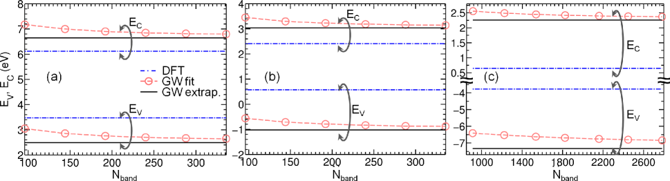
For the electronic excitation energies, the calculations are done with a full-frequency, spectrum-only self consistent approach, as implemented in VASP Shishkin and Kresse (2006, 2007). These specific choices in the method are based on previous results for the energy band alignment at the interface where this level of self consistency gave calculated band offsets within 0.3 eV of measured values Shaltaf et al. (2008). Convergence with respect to the number of empty states is achieved by a hyperbolic fit to a series of calculations and extrapolation Friedrich et al. (2011); Sup For the case of water, electronic states of the 32-molecule cell are analyzed for a sample of 50 snapshots over a 5 ps period, using for a subset of 12 snapshots with the same energy gap distribution.
With this level of the theory, as expected Shishkin and Kresse (2007), the calculated bulk band gaps of GaN (4.00 eV) and ZnO (3.93 eV) are somewhat too large in comparison to experiment (3.44 and 3.3 eV, respectively) Vurgaftman and Meyer (2003); Srikant and Clarke (1998), all at room temperature Sup . Also, as noted above, the optimized GaN and ZnO lattice constants are about 1% smaller than the experimental values, which contributes a 0.2-0.3 eV increase to the band gap through the deformation potentials Vurgaftman and Meyer (2003). For bulk water, the calculated average band gap based on DFT is 4.35 eV while the present approach gives 9.53 eV, slightly larger than the experimental value of eV Bernas et al. (1997). Our use of spectrum-only self consistency accounts for the increase relative to the recent result (8.1 eV Pham et al. (2014)). Furthermore, the binding energies of the occupied band and band relative to the band (see Fig. 3) are much more accurate in the present calculations (2.34 eV and 6.30 eV) than for the DFT energies (2.05 eV and 5.66 eV) in comparison to photoemission experiments (2.34 eV and 6.21 eV) Winter et al. (2004).
Next, we analyze the ingredients for the simple picture of Fig. 1a. From the MD simulation of a water slab Sup we find at the water-vacuum interface, in good agreement with earlier studies Leung (2010); Kathmann et al. (2011); Pham et al. (2014); Lucking et al. (2014). Using this value, the calculated bulk DOS for water is aligned relative to the vacuum level and compared with the experimental PES Winter et al. (2004) in Fig. 3. The binding energies are underestimated in DFT while the corrected binding energies are in very good agreement with the experimental data, particularly the level (peak centroid) at eV, compared to the measured value of eV Winter et al. (2004). For the clean GaN and ZnO surfaces, including relaxation, the valence band edge with respect to vacuum is calculated to be eV and eV, respectively. We make direct comparison to photoemission experiments for the closely related ZnO surface, for which we calculated eV, in good agreement, for an absolute energy, with the measured value, eV Swank (1967). See Ref. Stevanovic et al. (2014) for a broader survey. From these calibration examples for both ZnO and water, the highest occupied level is slightly too deep relative to vacuum, an error that partially cancels in the final theoretical results for the band alignment below. Overall, this suggests that errors in the band alignment at the aqueous interface will be similar to those found previously for the interface with the same level of self consistency Shaltaf et al. (2008).
The alignment of to the level in water according to the simplified scheme is shown in Fig. 4a (). The results for the ideal, unrelaxed semiconductor surfaces are also shown (). Relaxation leads to rotation of the surface bond with outward (inward) displacement of the anion (cation) and an induced dipole at the surface pointing inwards (Fig. 4b) which lowers relative to vacuum. This is a much larger effect for ZnO due to its more ionic bond.
Next we show the results from the full calculation, including the structure of the semiconductor-water interface (Fig. 1b). The calculated offsets () are placed on the vacuum scale using the calculated value for the level from the water slab calculation (Fig. 4a, ). For GaN, the change from the simple model is substantial, with shifting to eV. For ZnO, the degree of interface water dissociation is quantitatively important, with the final placement of being eV and eV for 50% and 67% dissociation, respectively. In contrast to the GaN case, the simple model for ZnO is surprisingly close to the overall result from the full calculation. Analysis of the induced surface dipoles shows opposing effects from the molecular and dissociative adsorption of water (Fig. 4c, d). For GaN, lifting the surface reconstruction is dominated by dissociative adsorption of water which lowers . For ZnO, the effect of lifting the reconstruction is larger while the mixture of molecular and dissociative water adsorption compete, with the latter being more significant in the 67% dissociative case.

To obtain more insight into the role of interface structure motifs, we show results in Fig. 4a () for each semiconductor with a single monolayer of adsorbed water in vacuum, with the degree of dissociation found at the full interface. The structures are fully relaxed, representative of a surface experiment. The result for GaN, eV, is rather close to the full calculation. This suggests that the additional dipole induced by interaction of the hydroxylated surface with liquid water is minimal. On the other hand, the results for the ZnO case ( and eV) agrees somewhat less well with the full calculations. Interestingly, key interface cation-O and O-H bond orientations fluctuate much more in the ZnO case compared to the GaN case. Correspondingly, the impact of the dipole contribution from the liquid water interface to the hydroxylated surface is also larger, another interface structure specific result. However, our results do suggest that a well-chosen, hydroxylated surface may be a better choice for application of the simple picture in Fig. 1a for semiconductors that actively promote water dissociation.
Electrochemical experiments for GaN Kocha et al. (1995); Beach et al. (2003) and for ZnO Gomes and Cardon (1982); Matsumoto et al. (1989) show acid-base activity at the semiconductor-water interface, with a clear rise of the measured band edge positions with solution pH (from 47 to 55 meV per pH unit, close to the ideal, Nernstian case of 59 meV). Therefore, an additional measurement must determine the pH at which the interface is neutral, assuring the equivalent of flat-band conditions on the water side of the junction. This has not been measured for GaN, but it is in the range of pH = 8 to 10 for ZnO Blok and De Bruyn (1970); Kunze et al. (2011). Taken together with the measured potential for the band edges Gomes and Cardon (1982); Matsumoto et al. (1989), the data are tightly clustered and relatively independent of facet, covering a range of about 0.3 eV, centered on = eV relative to vacuum. With reference to Fig. 4a, the value of from experiment is at higher energy than that predicted here for the ZnO interface with a partially dissociated water layer. It is also above the value from the simple picture of Fig. 1a, (experimental value, eV). Considering the impact on the dipole of different species at the interface (Fig. 4), this suggests that under realistic electrochemical conditions, another structural element with opposite dipole to the net effect seen here must be involved. Possibilities include alternative structures that result from etching of the ZnO or the role of adsorption of other ions from solution, both factors discussed in early literature Gomes and Cardon (1982); Blok and De Bruyn (1970); Dewald (1960).
In summary, we demonstrate the integrated use
of state-of-the-art techniques
for the first-principles treatment of energy level
alignment at aqueous semiconductor interfaces.
The initial, calibrated applications to
GaN and ZnO ,
which exhibit different degrees of both water dissociation
and cation-O and O-H bond fluctuations at the interface,
demonstrate the significant role of interface structure and dynamics.
In the future, this approach will support improved microscopic
understanding of chemical interactions and the impact of interface
structure on the fundamental energy alignments across semiconductor-water interfaces.
We thank P. B. Allen, M. Fernandez-Serra, D. Lu, and Y. Li for valuable discussions. This work was carried out at Brookhaven National Laboratory under contract No. DE-AC02-98CH10886 with the U.S. Department of Energy, supported by its Office of Basic Energy Sciences (Computational Materials and Chemical Sciences Network program, Division of Chemical Sciences and Scientific User Facilities Division), and utilized resources at the Center for Functional Nanomaterials, Brookhaven National Laboratory, and at the National Energy Research Scientific Computing Center, supported by the Office of Science of the U.S. Department of Energy under Contract No. DE-AC02-05CH11231.
References
- Franciosi and Van de Walle (1996) A. Franciosi and C. G. Van de Walle, Surf. Sci. Rep. 25, 1 (1996).
- Cheng and Sprik (2012) J. Cheng and M. Sprik, Phys. Chem. Chem. Phys. 14, 11245 (2012).
- Nozik and Memming (1996) A. J. Nozik and R. Memming, J. Phys. Chem. 100, 13061 (1996).
- Kudo and Miseki (2009) A. Kudo and Y. Miseki, Chem. Soc. Rev. 38, 253 (2009).
- Butler and Ginley (1978) M. A. Butler and D. S. Ginley, J. Electrochem. Soc. 125, 228 (1978).
- Winter et al. (2004) B. Winter, R. Weber, W. Widdra, M. Dittmar, M. Faubel, and I. V. Hertel, J. Phys. Chem. A 108, 2625 (2004).
- Trasatti (1986) S. Trasatti, Pure Appl. Chem. 58, 955 (1986).
- Cheng and Sprik (2010) J. Cheng and M. Sprik, Phys. Rev. B 82, 081406 (2010).
- Wu et al. (2011) Y. Wu, M. K. Y. Chan, and G. Ceder, Phys. Rev. B 83, 235301 (2011).
- Cheng and Selloni (2010) H. Cheng and A. Selloni, Langmuir 26, 11518 (2010).
- Jones and Gunnarsson (1989) R. O. Jones and O. Gunnarsson, Rev. Mod. Phys. 61, 689 (1989).
- Hybertsen and Louie (1986) M. S. Hybertsen and S. G. Louie, Phys. Rev. B 34, 5390 (1986).
- Godby et al. (1987) R. W. Godby, M. Schlüter, and L. J. Sham, Phys. Rev. B 35, 4170 (1987).
- Aulbur et al. (2000) W. G. Aulbur, L. Jonsson, and J. W. Wilkins, “Quasiparticle calculations in solids,” in Solid State Physics, vol. 54, edited by H. Ehrenreich and F. Spaepen (Academic, New York, 2000) pp. 1–218.
- Swartz and Wu (2013) C. W. Swartz and X. Wu, Phys. Rev. Lett. 111, 087801 (2013).
- Pham et al. (2014) T. A. Pham, C. Zhang, E. Schwegler, and G. Galli, Phys. Rev. B 89, 060202 (2014).
- Toroker et al. (2011) M. C. Toroker, D. K. Kanan, N. Alidoust, L. Y. Isseroff, P. Liao, and E. A. Carter, Phys. Chem. Chem. Phys. 13, 16644 (2011).
- Li et al. (2013) Y. Li, L. E. O’Leary, N. S. Lewis, and G. Galli, J. Phys. Chem. C 117, 5188 (2013).
- Stevanovic et al. (2014) V. Stevanovic, S. Lany, D. S. Ginley, W. Tumas, and A. Zunger, Phys. Chem. Chem. Phys. 16, 3706 (2014).
- Van de Walle and Martin (1986) C. G. Van de Walle and R. M. Martin, Phys. Rev. B 34, 5621 (1986).
- Zhang et al. (1988) S. B. Zhang, D. Tomanek, S. G. Louie, M. L. Cohen, and M. S. Hybertsen, Solid State Comm. 66, 585 (1988).
- Hybertsen (1991) M. S. Hybertsen, Appl. Phys. Lett. 58, 1759 (1991).
- Shaltaf et al. (2008) R. Shaltaf, G. M. Rignanese, X. Gonze, F. Giustino, and A. Pasquarello, Phys. Rev. Lett. 100, 186401 (2008).
- Lax (1952) M. Lax, J. Chem. Phys. 20, 1752 (1952).
- Cardona and Thewalt (2005) M. Cardona and M. L. W. Thewalt, Rev. Mod. Phys. 77, 1173 (2005).
- Soper and Benmore (2008) A. K. Soper and C. J. Benmore, Phys. Rev. Lett. 101, 065502 (2008).
- Maeda et al. (2006) K. Maeda, K. Teramura, D. L. Lu, T. Takata, N. Saito, Y. Inoue, and K. Domen, Nature 440, 295 (2006).
- Wang et al. (2011a) D. F. Wang, A. Pierre, M. G. Kibria, K. Cui, X. G. Han, K. H. Bevan, H. Guo, S. Paradis, A. R. Hakima, and Z. T. Mi, Nano Lett. 11, 2353 (2011a).
- Kharche et al. (2014) N. Kharche, M. S. Hybertsen, and J. T. Muckerman, Phys. Chem. Chem. Phys. 16, 12057 (2014).
- Blöchl (1994) P. E. Blöchl, Phys. Rev. B 50, 17953 (1994).
- Kresse and Furthmuller (1996) G. Kresse and J. Furthmuller, Phys. Rev. B 54, 11169 (1996).
- Kresse and Joubert (1999) G. Kresse and D. Joubert, Phys. Rev. B 59, 1758 (1999).
- Jensen et al. (2008) L. L. Jensen, J. T. Muckerman, and M. D. Newton, J. Phys. Chem. C 112, 3439 (2008).
- Dion et al. (2004) M. Dion, H. Rydberg, E. Schroder, D. C. Langreth, and B. I. Lundqvist, Phys. Rev. Lett. 92, 246401 (2004).
- Klimes et al. (2011) J. Klimes, D. R. Bowler, and A. Michaelides, Phys. Rev. B 83, 19513 (2011).
- (36) Springer Materials, Landolt-Bornstein Database , http://www.springermaterials.com/docs/index.html.
- (37) See Supplemental Material, which includes plots that illustrate the core potential offsets as a function of time and the extrapolation of the GW calculations versus number of empty states.
- Shen et al. (2010) X. A. Shen, Y. A. Small, J. Wang, P. B. Allen, M. V. Fernandez-Serra, M. S. Hybertsen, and J. T. Muckerman, J. Phys. Chem. C 114, 13695 (2010).
- Wang et al. (2011b) J. Wang, G. Roman-Perez, J. M. Soler, E. Artacho, and M. V. Fernandez-Serra, J. Chem. Phys. 134 (2011b).
- Dulub et al. (2005) O. Dulub, B. Meyer, and U. Diebold, Phys. Rev. Lett. 95, 136101 (2005).
- Tocci and Michaelides (2014) G. Tocci and A. Michaelides, J. Phys. Chem. Lett. 5, 474 (2014).
- Shishkin and Kresse (2006) M. Shishkin and G. Kresse, Phys. Rev. B 74, 035101 (2006).
- Shishkin and Kresse (2007) M. Shishkin and G. Kresse, Phys. Rev. B 75, 235102 (2007).
- Friedrich et al. (2011) C. Friedrich, M. C. Muller, and S. Blugel, Phys. Rev. B 83, 081101 (2011).
- Vurgaftman and Meyer (2003) I. Vurgaftman and J. R. Meyer, J. Appl. Phys. 94, 3675 (2003).
- Srikant and Clarke (1998) V. Srikant and D. R. Clarke, J. Appl. Phys. 83, 5447 (1998).
- Bernas et al. (1997) A. Bernas, C. Ferradini, and J. P. Jay-Gerin, Chem. Phys. 222, 151 (1997).
- Leung (2010) K. Leung, J. Phys. Chem. Lett. 1, 496 (2010).
- Kathmann et al. (2011) S. M. Kathmann, I.-F. W. Kuo, C. J. Mundy, and G. K. Schenter, J. Phys. Chem. B 115, 4369 (2011).
- Lucking et al. (2014) M. Lucking, Y.-Y. Sun, D. West, and S. Zhang, Chem. Sci. 5, 1216 (2014).
- Swank (1967) R. K. Swank, Phys. Rev. 153, 844 (1967).
- Kocha et al. (1995) S. S. Kocha, M. W. Peterson, D. J. Arent, J. M. Redwing, M. A. Tischler, and J. A. Turner, J. Electrochem. Soc. 142, L238 (1995).
- Beach et al. (2003) J. D. Beach, R. T. Collins, and J. A. Turner, J. Electrochem. Soc. 150, A899 (2003).
- Gomes and Cardon (1982) W. P. Gomes and F. Cardon, Progr. Surf. Sci. 12, 155 (1982).
- Matsumoto et al. (1989) Y. Matsumoto, T. Yoshikawa, and E. Sato, J. Electrochem. Soc. 136, 1389 (1989).
- Blok and De Bruyn (1970) L. Blok and P. L. De Bruyn, J. Colloid Interf. Sci. 32, 518 (1970).
- Kunze et al. (2011) C. Kunze, M. Valtiner, R. Michels, K. Huber, and G. Grundmeier, Phys. Chem. Chem. Phys. 13, 12959 (2011).
- Dewald (1960) J. F. Dewald, J. Phys. Chem. Sol. 14, 155 (1960).
I Supplemental Material
I.1 Methods used and technical details for the calculations
We have recently analyzed the atomic-scale structure at aqueous GaN and ZnO interfaces using DFT-based MD simulations, demonstrating the role of interface water dissociation Kharche et al. (2014) and establishing the technical protocol used here. DFT calculations are done using the projector augmented wave (PAW) method Blöchl (1994) as implemented in VASP Kresse and Furthmuller (1996); Kresse and Joubert (1999). The semicore levels for Ga and Zn are explicitly treated and the DFT+U method is employed with = 3.9 eV and = 6.0 eV for the orbitals Jensen et al. (2008). The Born-Oppenheimer MD simulations are performed using a Nose-Hoover thermostat and a Verlet integrator with a time step of 0.5 fs. The functional optB88-vdW Dion et al. (2004); Klimes et al. (2011), including long-range van der Waals interactions, together with a slightly elevated temperature (T = 350 K), gives an accurate O-O pair distribution function and diffusivity. Converged results require a plane-wave cutoff energy of 600 eV. All calculations are carried out at the optimized bulk lattice constants: For GaN, and and for ZnO, and . These agree with the experimental values to within 1.3 % Lan . MD simulations are run for 10 to 20 ps and analysis is performed for 5 ps thermalized windows.
The reference cell for bulk liquid water contains 32 molecules (9.86 ). The GaN-water interface is simulated using a repeated supercell in which a 12 layer slab of oriented wurtzite-structure semiconductor with a lateral cell alternates with a water filled region containing 81 water molecules. The statistical information in (Fig. 2b-d) is obtained using the geometrical criteria described in our earlier work Kharche et al. (2014). Excluding 3 Å thick surface layers, the O-O pair distribution function, hydrogen bond network, and valence band DOS are close to those calculated for bulk water. The average density is slightly too large (). The band remained at the same energy relative to the core potential due to cancellation in deformation potentials. For the ZnO interface, the interface water layer is partially dissociated. Half of the adsorbed water molecules dissociate for a interface cell simulated with 66 water molecules. For a cell with 49 water molecules, in-plane boundary conditions result in fluctuations in the fraction of water dissociated at the interface, including intervals where it is 67%, providing another structure for study. Finally, the water-vacuum interface is modeled using a supercell of the same size as that used for the GaN-water interface simulation. In the supercell, an approximately 25 thick water layer containing 69 water molecules alternates with about 16 thick vacuum region..

Calculations sampling the electronic structure from the MD simulations naturally include the impact of finite temperature renormalization of the energy levels, albeit in a semiclassical approximation Lax (1952); Cardona and Thewalt (2005). Although it is a relatively small effect in the semiconductors at room temperature, for consistency with the treatment of liquid water, we include them. Specifically data from MD simulations for 12 layer, bulk supercells of GaN and ZnO show a band gap renormalization of and eV respectively.
I.2 Electrostatic potential offset as a function of the simulation time
As described in the main text, we employ the PAW core potential as a reference to calculate the interface potential offset () as a function of the MD simulation time. Specifically, the PAW core potentials are based on charge of radius (0.95, 1.03, 0.72) Å for (Zn, Ga, O). Here we show the trajectories for all the aqueous interfaces studied in this work, Figs. S1-S3, and provide further details of the supercells studied and the impact of the thickness of the water region. The potential offset for the clean semiconductor surfaces and the semiconductor surfaces with 1 ML of water adsorbed were calculated from a single, static structure with the relaxation specified in the text.
The starting atomic configuration for the water-vacuum interface (Fig. S1) is obtained by removing the GaN slab and the adsorbed water molecules from a snapshot taken from the equilibrated portion of the MD trajectory of a cell containing GaN slab and 81 water molecules. This provides a well equilibrated water layer although with different surface boundary conditions. The MD trajectory after 2 ps equilibration is used to calculate the electrostatic potential offsets by averaging all snapshots within 1.25 ps windows. In Fig. S1 the values (, , , eV) depicted by the horizontal solid grey lines average to eV (black dashed line) with the standard deviation of 0.072 eV (vertical error bar).
For the data from the GaN-water interface in Fig. S2, the same averaging scheme as that in Fig. S1 is used. The MD simulation is started with a smaller cell containing 48 water molecules. The starting atomic configuration for a larger cell containing 81 water molecules is prepared by inserting a 33 water molecule slab at the ambient density in the middle of the water layer in an equilibrated snapshot of a smaller cell containing 48 water molecules.
In Fig. S2a, the values (, , , , , eV) depicted by the horizontal solid grey lines average to -6.86 eV (black dashed line) with the standard deviation of 0.054 eV (vertical error bar). In Fig. S2b, the values (, , , eV) depicted by the horizontal solid grey lines average to eV (black dashed line) with the standard deviation of 0.054 eV (vertical error bar). Thus, the GaN-water electrostatic potential offset is well converged with respect to the thickness of the water layer.
For the data from the ZnO-water interface in Fig. S3, the same averaging scheme as that in Fig. S1 is used except only the snapshots corresponding to the symmetric 50 or 67% water dissociation on both bottom and top interfaces are included. Symmetric dissociation patterns are selected to avoid complications due to the residual electric fields in the semiconductor slab and the bulk water region. The MD simulation using () interface cell is started with a cell containing 49 (66) water molecules. The starting atomic configuration for a larger cell containing 82 water molecules is obtained using the same procedure as described in Fig. S2.
In Fig. S3a, the values (, , , eV) for 50% water dissociation depicted by the horizontal solid light blue lines average to eV (blue dashed line) with the standard deviation of 0.095 eV (vertical error bar) while the values (, , , , eV) for 67% water dissociation depicted by the horizontal solid light red lines average to eV (red dashed line) with the standard deviation of 0.073 eV (vertical error bar). These data are used to report the comparison between 50% and 67% dissociated interfaces in Fig. 4a of the main text.
In Fig. S3b, the values (, , eV) for 67% water dissociation depicted by the horizontal solid light red lines average to eV (red dashed line) with the standard deviation of 0.046 eV (vertical error bar).
In Fig. S3c, the values (, , , , , eV) for 50% water dissociation depicted by the horizontal solid light blue lines average to eV (blue dashed line) with the standard deviation of 0.040 eV (vertical error bar).
Comparing the 67% water dissociation in Fig. S3a and Fig. S3b, the ZnO-water electrostatic potential offset variation changes with respect to the thickness of the water layer by somewhat less than 0.15 eV. Evidently the details of the transient stabilization of this interface structure depend on nearby water or proximity to the other interface. Even though the interval of transient stabilization of 50% water dissociation in Fig. S3a is smaller, the electrostatic potential offset agrees quite well with that found in Fig. S3c, for the interface structure. Without artificial constraints in the boundary conditions, the 50% structure is likely more stable.
I.3 Convergence of results
In the self-consistency, six cycles are sufficient for convergence to 0.05 eV. An energy cutoff of 150 eV is used for the response function calculations. We converged the results relative to the number of empty states included using several calculations with ca. 5 to 20 times the number of occupied states together with a hyperbolic fit to extrapolate to the infinite limit Friedrich et al. (2011). The hyperbolic function used is
| (2) |
where is the total number bands and , , and are fitting parameters. The results are shown in Fig. S4 for GaN, ZnO, and one snapshot from the MD simulation of the water cell containing 32 water molecules. To obtain the density of states (DOS) of water shown in the bottom panel of Fig. 3 of the main text, we used the same hyperbolic fitting method to extrapolate all valence band states from 12 MD snapshots and averaged the results. Note that the convergence of the valence and conduction band edges separately is considerably slower compared to the band gap.
References
- Kharche et al. (2014) N. Kharche, M. S. Hybertsen, and J. T. Muckerman, Phys. Chem. Chem. Phys. 16, 12057 (2014).
- Blöchl (1994) P. E. Blöchl, Phys. Rev. B 50, 17953 (1994).
- Kresse and Furthmuller (1996) G. Kresse and J. Furthmuller, Phys. Rev. B 54, 11169 (1996).
- Kresse and Joubert (1999) G. Kresse and D. Joubert, Phys. Rev. B 59, 1758 (1999).
- Jensen et al. (2008) L. L. Jensen, J. T. Muckerman, and M. D. Newton, J. Phys. Chem. C 112, 3439 (2008).
- Dion et al. (2004) M. Dion, H. Rydberg, E. Schroder, D. C. Langreth, and B. I. Lundqvist, Phys. Rev. Lett. 92, 246401 (2004).
- Klimes et al. (2011) J. Klimes, D. R. Bowler, and A. Michaelides, Phys. Rev. B 83, 19513 (2011).
- (8) Springer Materials, Landolt-Bornstein Database , http://www.springermaterials.com/docs/index.html.
- Lax (1952) M. Lax, J. Chem. Phys. 20, 1752 (1952).
- Cardona and Thewalt (2005) M. Cardona and M. L. W. Thewalt, Rev. Mod. Phys. 77, 1173 (2005).
- Friedrich et al. (2011) C. Friedrich, M. C. Muller, and S. Blugel, Phys. Rev. B 83, 081101 (2011).