Electrostatic Coupling between Two Surfaces of a Topological Insulator Nanodevice
Abstract
We report on electronic transport measurements of dual-gated nano-devices of the low-carrier density topological insulator . In all devices the upper and lower surface states are independently tunable to the Dirac point by the top and bottom gate electrodes. In thin devices, electric fields are found to penetrate through the bulk, indicating finite capacitive coupling between the surface states. A charging model allows us to use the penetrating electric field as a measurement of the inter-surface capacitance and the surface state energy-density relationship , which is found to be consistent with independent ARPES measurements. At high magnetic fields, increased field penetration through the surface states is observed, strongly suggestive of the opening of a surface state band gap due to broken time-reversal symmetry.
pacs:
73.20.Fz, 72.15.Rn, 73.25.+i,85.30.Tv,84.37.+qThree dimensional topological insulators (3D TIs) have been undergoing intense theoretical and experimental research on the properties of their unique surface states Hasan and Kane (2010); Qi and Zhang (2011). The presence of bulk carriers has hampered experimental progress, so a variety of crystal growth Hor et al. (2009); Zhang et al. (2011); Ren et al. (2010, 2011); Kong et al. (2011); Gehring et al. (2012) and in-situ charge displacement techniques Steinberg et al. (2010); Checkelsky et al. (2011); Yuan et al. (2011); Kim et al. (2012a); Segawa et al. (2012) have been applied to suppress bulk conductivity. For example, quaternary TI materials of the form have a significantly suppressed bulk contribution to transport, reaching large bulk resistivities and insulating-like temperature dependence Ren et al. (2011); Arakane et al. (2012); Taskin et al. (2011). Furthermore, exfoliation or growth of thin crystals has been used to achieve surface-dominated transport Lee et al. (2012); Kong et al. (2011); Kim et al. (2012a); Xia et al. (2013); Gehring et al. (2012). However, amid the extensive experimental effort on TI device transport, there is no study reporting independent control over the density of both the upper and lower surface states in a single TI device. A full understanding of transport phenomena in TIs, such as the quantum Hall Tilahun et al. (2011); Vafek (2011) and Josephon effects Williams et al. (2012); Veldhorst et al. (2012); Rokhinson et al. (2012), will require independent tuning of the density of each surface state. Additionally, proposals for topological exciton condensates explicitly require fine tuning the density of both surfaces Seradjeh et al. (2009), and finite displacement fields from two gates can affect the quantum anomalous Hall effect in TI-based systems Yu et al. (2010); Chang et al. (2013).
In this Letter, we report electronic transport measurements of exfoliated (BSTS) nanodevices with top and bottom gate electrodes. We show for the first time that the chemical potential of the upper and lower surface states can be controlled independently, resulting in different resistance peaks when either surface chemical potential crosses the Dirac point. For thin devices, we find signatures of finite capacitive coupling between the surface states, consistent with fully depleted bulk states. We explain the data through a charging model which incorporates the finite density of states of the surface bands. Using angle-resolved photoemission spectroscopy (ARPES) as a control measurement of the surface state, this model allows us to measure the chemical potential and charge density of a topological surface state as well as the inter-surface capacitance . At high magnetic fields, increased field penetration through the surface states is observed, strongly suggestive of the opening of a surface state band gap.
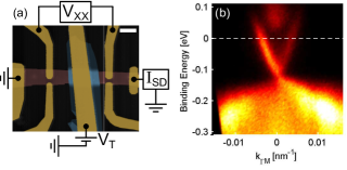
BSTS was prepared by melting high purity samples of the constituent elements in a sealed quartz ampoule under inert atmosphere. Sample structure was confirmed by x-ray powder diffraction, and large single crystals showed similar bulk transport behavior to previous reports Ren et al. (2011). Static ARPES shows that the chemical potential is inside the bulk band gap and that the Dirac point energy is above the bulk valence band edge (see SM SMO ). Pump-probe time-resolved ARPES (TrARPES) allows access to unoccupied states as shown in Fig. 1b Sobota et al. (2012); Wang et al. (2012). The Fermi velocity near the Dirac point is , and the band gap at room temperature is . Note that the surface state dispersion is strongly electron-hole asymmetric. These data are consistent with previous experiments Arakane et al. (2012); Kim et al. (2014).
Thin flakes for transport studies were obtained by mechanical exfoliation onto a doped silicon wafer with a 285nm thick thermal surface layer that serves as the bottom gate electrode and dielectric, respectively. A thin layer of hexagonal boron nitride (h-BN) was mechanically transferred on top to serve as the top gate dielectric Dean et al. (2010). Thermally evaporated Ti/Au layers were used to make ohmic contacts and top gate electrodes. Atomic Force Microscopy was used to determine the thickness of the BSTS and h-BN layers. For all data presented here, a four-probe voltage measurement was used determine the 2D resistivity. Here we report results measured on BSTS devices of different thicknesses: device A is 42 nm, and device B is 82 nm. The behavior of device A was reproduced in a third device SMO . All three devices were fabricated from flakes from the same exfoliation, and therefore from the same region of the bulk crystal. Fig. 1a, shows an AFM image of device A.
On devices A and B, both the top and bottom gates easily tune the device through a resistance peak () by adjusting the applied voltages and , respectively, as shown in Fig. 2a-b. is associated with a minimum in carrier density (i.e. the surface Dirac point), as confirmed via the Hall effect SMO . Interestingly, the top-gate is observable up to room temperature; in contrast, for the bottom gate changes into a broad S-shape, consistent with gating studies of other TIs using gate dielectrics Checkelsky et al. (2011); Xia et al. (2013); Kong et al. (2011). The disappearance of a distinct resistance peak in the limit of strong disorder was predicted by recent theories for TI surface states with electron-hole asymmetry Adam et al. (2012), suggesting that the difference in the field-effect behavior may be related to the disorder profile at the interface. Strong differences in the disorder profile at and h-BN interfaces have been observed in graphene Xue et al. (2011).
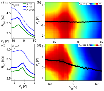
Two-dimensional maps of the resistivity with respect to both top and bottom gate voltage reveal a distinct difference in the behavior of devices A and B, shown in Fig. 2d and 2c, respectively. The black dots identify , the top gate voltage at which is found, at each . We associate with charge neutrality of the upper surface state: . For device B, is independent of , demonstrating no capacitive coupling between the upper surface and the bottom gate electrode. The fact that thicker devices do not have this capacitive coupling suggests that mobile bulk electronic states exist in the interior. By contrast, in device A is dependent on . The observed relationship means that there exists a finite and non-constant capacitive coupling between the upper surface and the bottom gate. This capacitive coupling requires field penetration through the lower surface state and the interior of the thinner crystal, which fail to completely screen electric fields. The contrasting gating behavior of the devices is corroborated by the temperature dependence of their resistivities (see SM SMO ). We also note that while dual-gated TI devices have been previously reported Kim et al. (2012a); Checkelsky et al. (2012), the devices reported here are unique in that the two surface states are tuned independently and separately observed.
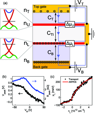
Here we focus on the capacitive coupling between the bottom gate and the upper surface in the thin crystal, and data regarding coupling of the top gate and lower surface are presented in the SM SMO . The slope of is a measure of the ratio of the capacitive coupling of the bottom and top gates to the upper surface, which includes partial screening of electric fields by the lower surface state. At the slope of and the resistance of the lower surface are simultaneously at a maximum, i.e. near the Dirac point (see Fig. 3b). This is consistent with a minimum in the screening effectiveness of the lower surface state at the Dirac point. Understanding this behavior quantitatively requires a detailed charging model, which we discuss below.
By considering the BSTS surface states as a grounded pair of 2D electronic states, the general gating behavior can be understood via a charging model construction originally developed for parallel graphene layers Kim et al. (2012b). This model is schematically represented in Fig. 3a, where the important quantities are the applied gate voltages (, ), the geometric capacitances per unit area of the gates (, ), the inter-surface capacitance per unit area (), the charge densities of the gate electrodes (, ), and the charge density and chemical potentials of the lower (, ) and upper (, ) surface states. Four coupled equations completely describe the charging of the system: one from charge neutrality, and three from Faraday’s law, which restricts the sum of voltage drops around a loop to equal zero, which includes the change in chemical potential of the surface states , where is the initial Fermi energy relative to the Dirac point for surface state . A detailed derivation is provided in the SM SMO . For this study, we are interested in the condition that the chemical potential at the upper surface is at the Dirac point. By setting and , a useful pair of equations can be derived:
| (1) | |||||
| (2) |
where , and are constants that depend on the initial densities and chemical potentials of the two surfaces (see SM SMO ). Equations 1 and 2 serve as a linear transformation from a trajectory in gate voltage space (Fig. 3b) to a relationship between chemical potential and density for the lower surface state (Fig. 3c).
Experimentally, three unknowns remain: the inter-surface capacitance and the initial offset carrier densities of the upper and lower surfaces . To constrain these parameters, an independent measurement of is required. ARPES measurements of the surface state band structure can be easily converted to a model for , including an explicit treatment of the bulk states SMO . A three-parameter least-squares fit between the transformation of the transport data and the ARPES model is performed and shown in Fig. 3c SMO . The inter-layer capacitance from this fit is , corresponding to an effective bulk permittivity of , comparable to values for similar compounds Collaboration: Authors and editors of the volumes III/17E-17F-41C ; Petzelt and Grigas (1973); Richter and Becker (1977). The initial electron densities of the upper and lower surface states are found to be and , which agrees well with values simply calculated from the magnitude of and necessary to reach the resistance peaks.
It is important to note that can be affected in a few ways. For example, localized electronic states could polarize, increasing . As another possibility, low-density, poorly conducting bulk states could weakly screen electric fields, reducing . However, in the thin limit the surface states should efficiently screen charged bulk impurities, resulting in an absence of charged puddles of bulk states at charge neutrality for crystals of thickness Skinner et al. (2013). This length scale is consistent with the observation that device B ( thick) appears to have conducting states screening the two surfaces from each other.
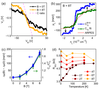
We now turn to the behavior of the thin device in high magnetic fields. The Hall mobility of this sample is low, of order ; as a result, no evidence of Landau levels is found, and a clear remains. Nevertheless, the charging behavior of the device changes significantly at finite field. Fig. 4a shows of the upper surface at and . is affected by much more strongly at 8T. Assuming does not change, equations 1 and 2 can be applied without changing parameters, as shown in Fig. 4b (blue dots). For the same total change in charge density, the total chemical potential change of the lower surface is about 60% larger. More precisely, the chemical potential appears to change more rapidly at low carrier densities, indicating a distinctly smaller thermodynamic density of states. Fig. 4c (left axis) shows the difference in total chemical potential change as a function of magnetic field. The energy difference increases roughly quadratically with magnetic field. A possible interpretation is that the surface states develop a band gap that forms as a result of breaking time-reversal symmetry. While a non-linear magnetic field dependence would naively rule out a Zeeman-induced band gap, disorder will mask this effect at low fields when the gap is small Skinner et al. (2013), causing a non-linear increase in the apparent gap in the density of states. Detailed Shubnikov-de-Haas analysis of similar TI materials estimate a surface -factor in the range 40 to 80 Taskin and Ando (2011), which would be too small to explain this effect, although the g-factor has not yet been measured for this particular compound.
We further observe that the temperature dependence of resistivity also changes significantly at high magnetic fields. In Figure 4d, the temperature dependence of resistivity when both surfaces are at charge neutrality changes from metallic-like at zero magnetic field to non-metallic at high magnetic field, suggestive of a possible metal-insulator transition. This is consistent with the formation of a gap in the surface states with a high level of disorder. Similar non-metallic resistivity vs temperature curves were observed in bilayer graphene studies with similar band gaps in the high-disorder limit Oostinga et al. (2008).
However, we cannot rule out the possibility of an inter-surface magneto-capacitance. Restricting the model such that the total chemical potential change is the same as at zero magnetic field (i.e. a field-independent average density of states, see green curve in Fig. 4b), we find that must increase in magnetic field to compensate (Fig. 4c, right axis). increases in a similar way as the chemical potential difference because , as in equation 1. The raw bulk permittivity cannot explain this change, because the optical phonon spectra of related TI compounds show little change at similar magnetic fields Sushkov et al. (2010); LaForge et al. (2010). Electronic contributions to such as those mentioned earlier (polarizable localized states or weakly screening bulk states) could be modified by a magnetic field. In the supplement we show evidence that the effects of temperature and magnetic field separately affect and , respectively SMO , further suggesting that the magnetic field is modifying the density of states and not causing a magneto-capacitive effect.
In summary, exfoliated nanoflakes of BSTS are of sufficiently low total carrier density for both the upper and lower surface state densities to be independently modulated by electrostatic gates and for electric fields to penetrate through the bulk. Utilizing a model that captures the charging of the system, we measure the inter-surface capacitance as well as the energy-density relationship of the surface states, which agrees well with independent ARPES measurements. At high magnetic fields, increased field penetration is observed, strongly suggestive of band gap opening in the lower surface state.
This work was partly supported by the DOE, Basic Energy Sciences Office, Division of Materials Sciences and Engineering, under award DE-SC0006418 (VF, SE, HS, and PJH), by the Gordon and Betty Moore Foundation grant GBMF2931 and the STC Center for Integrated Quantum Materials, NSF grant DMR-1231319 (BH and RCA), and by an MIT MRSEC Initiative under NSF award DMR-0819762 (FM and NG). This work made use of the Materials Research Science and Engineering Center Shared Experimental Facilities supported by NSF under award DMR-0819762. Sample fabrication was performed partly at the Harvard Center for Nanoscale Science supported by the NSF under grant no. ECS-0335765. Sample synthesis and initial characterization were performed under LDRD (Tracking Code 12-ERD-013) at Lawrence Livermore National Laboratory (LLNL). LLNL is operated by Lawrence Livermore National Security, LLC, for the US Department of Energy, National Nuclear Security Administration, under Contract No. DE-AC52-07NA27344. We thank A. Stern, Y. Baum, K. Burch, D. Drew, B. Skinner, A. Frenzel, and J.D. Sanchez-Yamagishi for discussions and J. R. Jeffries for performing x-ray diffraction measurements.
References
- Hasan and Kane (2010) M. Z. Hasan and C. L. Kane, Rev. Mod. Phys. 82, 3045 (2010).
- Qi and Zhang (2011) X.-L. Qi and S.-C. Zhang, Rev. Mod. Phys. 83, 1057 (2011).
- Hor et al. (2009) Y. S. Hor, A. Richardella, P. Roushan, Y. Xia, J. G. Checkelsky, A. Yazdani, M. Z. Hasan, N. P. Ong, and R. J. Cava, Phys. Rev. B 79, 195208 (2009).
- Zhang et al. (2011) J. Zhang, C.-Z. Chang, Z. Zhang, J. Wen, X. Feng, K. Li, M. Liu, K. He, L. Wang, X. Chen, Q.-K. Xue, X. Ma, and Y. Wang, Nat Commun 2, 574 (2011).
- Ren et al. (2010) Z. Ren, A. A. Taskin, S. Sasaki, K. Segawa, and Y. Ando, Phys. Rev. B 82, 241306 (2010).
- Ren et al. (2011) Z. Ren, A. A. Taskin, S. Sasaki, K. Segawa, and Y. Ando, Phys. Rev. B 84, 165311 (2011).
- Kong et al. (2011) D. Kong, Y. Chen, J. J. Cha, Q. Zhang, J. G. Analytis, K. Lai, Z. Liu, S. S. Hong, K. J. Koski, S.-K. Mo, Z. Hussain, I. R. Fisher, Z.-X. Shen, and Y. Cui, Nat Nano 6, 705 (2011).
- Gehring et al. (2012) P. Gehring, B. F. Gao, M. Burghard, and K. Kern, Nano Lett. 12, 5137 (2012).
- Steinberg et al. (2010) H. Steinberg, D. R. Gardner, Y. S. Lee, and P. Jarillo-Herrero, Nano Lett. 10, 5032 (2010).
- Checkelsky et al. (2011) J. G. Checkelsky, Y. S. Hor, R. J. Cava, and N. P. Ong, Phys. Rev. Lett. 106, 196801 (2011).
- Yuan et al. (2011) H. Yuan, H. Liu, H. Shimotani, H. Guo, M. Chen, Q. Xue, and Y. Iwasa, Nano Lett. 11, 2601 (2011).
- Kim et al. (2012a) D. Kim, S. Cho, N. P. Butch, P. Syers, K. Kirshenbaum, S. Adam, J. Paglione, and M. S. Fuhrer, Nat Phys 8, 459 (2012a).
- Segawa et al. (2012) K. Segawa, Z. Ren, S. Sasaki, T. Tsuda, S. Kuwabata, and Y. Ando, Phys. Rev. B 86, 075306 (2012).
- Arakane et al. (2012) T. Arakane, T. Sato, S. Souma, K. Kosaka, K. Nakayama, M. Komatsu, T. Takahashi, Z. Ren, K. Segawa, and Y. Ando, Nat. Comm. 3, 636 (2012).
- Taskin et al. (2011) A. A. Taskin, Z. Ren, S. Sasaki, K. Segawa, and Y. Ando, Phys. Rev. Lett. 107 (2011), 10.1103/PhysRevLett.107.016801.
- Lee et al. (2012) J. Lee, J. Park, J.-H. Lee, J. S. Kim, and H.-J. Lee, Phys. Rev. B 86 (2012), 10.1103/PhysRevB.86.245321.
- Xia et al. (2013) B. Xia, P. Ren, A. Sulaev, P. Liu, S.-Q. Shen, and L. Wang, Phys. Rev. B 87, 085442 (2013).
- Tilahun et al. (2011) D. Tilahun, B. Lee, E. M. Hankiewicz, and A. H. MacDonald, Phys. Rev. Lett. 107, 246401 (2011).
- Vafek (2011) O. Vafek, Phys. Rev. B 84, 245417 (2011).
- Williams et al. (2012) J. R. Williams, A. J. Bestwick, P. Gallagher, S. S. Hong, Y. Cui, A. S. Bleich, J. G. Analytis, I. R. Fisher, and D. Goldhaber-Gordon, Phys. Rev. Lett. 109, 056803 (2012).
- Veldhorst et al. (2012) M. Veldhorst, M. Snelder, M. Hoek, T. Gang, V. K. Guduru, X. L. Wang, U. Zeitler, W. G. van der Wiel, A. A. Golubov, H. Hilgenkamp, and A. Brinkman, Nat Mater 11, 417 (2012).
- Rokhinson et al. (2012) L. P. Rokhinson, X. Liu, and J. K. Furdyna, Nat Phys 8, 795 (2012).
- Seradjeh et al. (2009) B. Seradjeh, J. E. Moore, and M. Franz, Phys. Rev. Lett. 103, 066402 (2009).
- Yu et al. (2010) R. Yu, W. Zhang, H.-J. Zhang, S.-C. Zhang, X. Dai, and Z. Fang, Science 329, 61 (2010), PMID: 20522741.
- Chang et al. (2013) C.-Z. Chang, J. Zhang, X. Feng, J. Shen, Z. Zhang, M. Guo, K. Li, Y. Ou, P. Wei, L.-L. Wang, Z.-Q. Ji, Y. Feng, S. Ji, X. Chen, J. Jia, X. Dai, Z. Fang, S.-C. Zhang, K. He, Y. Wang, L. Lu, X.-C. Ma, and Q.-K. Xue, Science 340, 167 (2013).
- (26) “See supplemental material at [url] for additional arpes data, data on a third device, hall effect data, gating behavior of conductance fluctuations, a detailed derivation of the charging model, and additional temperature- and magnetic field-dependence data.” .
- Sobota et al. (2012) J. A. Sobota, S. Yang, J. G. Analytis, Y. L. Chen, I. R. Fisher, P. S. Kirchmann, and Z.-X. Shen, Phys. Rev. Lett. 108, 117403 (2012).
- Wang et al. (2012) Y. H. Wang, D. Hsieh, E. J. Sie, H. Steinberg, D. R. Gardner, Y. S. Lee, P. Jarillo-Herrero, and N. Gedik, Phys. Rev. Lett. 109, 127401 (2012).
- Kim et al. (2014) S. Kim, S. Yoshizawa, Y. Ishida, K. Eto, K. Segawa, Y. Ando, S. Shin, and F. Komori, Phys. Rev. Lett. 112, 136802 (2014).
- Dean et al. (2010) C. R. Dean, A. F. Young, I. Meric, C. Lee, L. Wang, S. Sorgenfrei, K. Watanabe, T. Taniguchi, P. Kim, K. L. Shepard, and J. Hone, Nat Nano 5, 722 (2010).
- Adam et al. (2012) S. Adam, E. H. Hwang, and S. Das Sarma, Phys. Rev. B 85, 235413 (2012).
- Xue et al. (2011) J. Xue, J. Sanchez-Yamagishi, D. Bulmash, P. Jacquod, A. Deshpande, K. Watanabe, T. Taniguchi, P. Jarillo-Herrero, and B. J. LeRoy, Nat Mater 10, 282 (2011).
- Checkelsky et al. (2012) J. G. Checkelsky, J. Ye, Y. Onose, Y. Iwasa, and Y. Tokura, Nature Physics 8, 729 (2012).
- Kim et al. (2012b) S. Kim, I. Jo, D. C. Dillen, D. A. Ferrer, B. Fallahazad, Z. Yao, S. K. Banerjee, and E. Tutuc, Phys. Rev. Lett. 108, 116404 (2012b).
- (35) Collaboration: Authors and editors of the volumes III/17E-17F-41C, in Non-Tetrahedrally Bonded Elements and Binary Compounds I, Vol. 41C, edited by O. Madelung, U. Rössler, and M. Schulz (Springer-Verlag, Berlin/Heidelberg) pp. 1–4.
- Petzelt and Grigas (1973) J. Petzelt and J. Grigas, Ferroelectrics 5, 59 (1973).
- Richter and Becker (1977) W. Richter and C. R. Becker, physica status solidi (b) 84, 619–628 (1977).
- Skinner et al. (2013) B. Skinner, T. Chen, and B. I. Shklovskii, J. Exp. The. Phys. 117, 579 (2013).
- Taskin and Ando (2011) A. A. Taskin and Y. Ando, Phys. Rev. B 84, 035301 (2011).
- Oostinga et al. (2008) J. B. Oostinga, H. B. Heersche, X. Liu, A. F. Morpurgo, and L. M. K. Vandersypen, Nat Mater 7, 151 (2008).
- Sushkov et al. (2010) A. B. Sushkov, G. S. Jenkins, D. C. Schmadel, N. P. Butch, J. Paglione, and H. D. Drew, Phys. Rev. B 82, 125110 (2010).
- LaForge et al. (2010) A. D. LaForge, A. Frenzel, B. C. Pursley, T. Lin, X. Liu, J. Shi, and D. N. Basov, Phys. Rev. B 81, 125120 (2010).