Topological properties of linear circuit lattices
Abstract
Motivated by the topologically insulating (TI) circuit of capacitors and inductors proposed and tested in arXiv:1309.0878, we present a related circuit with less elements per site. The normal mode frequency matrix of our circuit is unitarily equivalent to the hopping matrix of a quantum spin Hall insulator (QSHI) and we identify perturbations that do not backscatter the circuit’s edge modes. The idea behind these models is generalized, providing a platform to simulate tunable and locally accessible lattices with arbitrary complex spin-dependent hopping of any range. A simulation of a non-Abelian Aharonov-Bohm effect using such linear circuit designs is discussed.
pacs:
42.70.Qs, 03.65.Vf, 78.67.PtThe realization that electrons propagating on edges of two-dimensional topological insulators at zero temperature are protected from certain disorder Kane and Mele (2005a, b); Sheng et al. (2005, 2006); Bernevig and Zhang (2006) has spurred research simulating these and similar edge effects in photonic/phononic systems Raghu and Haldane (2008); *wang2009; *koch2010; *umucalilar2011; *kraus2012b; *fang2012; *ochiai2012; *liangchong; *rechtsman2012; *rechtsman2013; *verbin2013; *lu2013; *davoyan2013; *peano2014; *nalitov2014; *wang2014a; *karzig2014; *bardyn2014; Hafezi et al. (2011); *mittal2014; Khanikaev et al. (2013); He et al. (reviewed in Lu et al. (2014)). The existence of edge modes whose energies lie within a given bulk gap of a noninteracting tight-binding Hamiltonian can be traced to a certain property of the corresponding hopping matrix Yu. Kitaev (2009). Namely, a topologically nontrivial hopping matrix is characterized by having a nontrivial value of some topological invariant at that bulk gap. Therefore, the problem of engineering edge modes in bosonic systems can be reduced to making sure that time evolution is governed by some topologically nontrivial matrix. Many efforts emulate the electronic systems that inspired us, but over time we should be able to construct a wider variety of systems than those readily available in nature (e.g. Stanescu et al. (2010)). While edge mode protection in topologically nontrivial bosonic systems may not be as intrinsic or robust (e.g. protection is not guaranteed by time-reversal symmetry; see Box 2 of Lu et al. (2014)), these directions should nevertheless advance understanding and could offer novel applications of the materials in question.
In this Letter, we discuss topologically insulating (TI) circuits Jia et al. – lattices of inductors and capacitors whose normal mode frequency matrix mimics a topologically nontrivial hopping matrix of an electronic system. Topological photonics includes many proposals Raghu and Haldane (2008); *wang2009; *koch2010; *umucalilar2011; *kraus2012b; *fang2012; *ochiai2012; *liangchong; *rechtsman2012; *rechtsman2013; *verbin2013; *lu2013; *davoyan2013; *peano2014; *nalitov2014; *wang2014a; *karzig2014; *bardyn2014; Hafezi et al. (2011); *mittal2014; here we study only inductors and capacitors with the goal of providing the simplest building blocks that can lead to topological nontriviality. We discuss a minimal example whose is (unitarily) equivalent to the hopping matrix of a spinful 2D electron gas in a magnetic field (see Sec. 5.2 in Bernevig and Hughes (2013)), i.e., a spin-doubled Azbel-Hofstadter model Azbel (1964); *hofstadter1976 (deemed the time-reversal invariant (TRI) Hofstadter model Cocks et al. (2012); *orth2013; *wang2014). Our example simulates magnetic flux per plaquette. Such a model is (topologically) similar to the spin-doubled Haldane model lattice Haldane (1988) (see Sec. 9.1.2 in Bernevig and Hughes (2013)) that is featured in the more general Kane-Mele topological insulator Kane and Mele (2005a, b). We determine how features of such models carry over to the circuit context, summarized in a table at the end of the article. The first TI circuit, which has already been realized Jia et al. , is a simple extension of our example and we outline that design in 11footnotemark: 100footnotetext: See Supplemental Material [URL], which includes Refs. Kibler (2009); Bosma et al. (1997), for a comparison of this work to Jia et al. as well as details on the non-Abelian generalization.. We further generalize the recipe and provide a method to construct equivalent to the hopping matrix of a lattice of spins with arbitrary complex spin-dependent hopping. Notably, we show how to simulate any hopping with a smaller circuit than that of Jia et al. , which simulated a specific hopping. This provides a platform to synthesize background gauge fields using linear circuits in parallel to studies with more complex elements Kapit (2013); *hafezi2014; Hafezi et al. (2011); *mittal2014 and to intense investigations using ultracold atoms (e.g. Gerbier et al. (2013); *aidelsburger2014; Osterloh et al. (2005); Jacob et al. (2007); Bermudez et al. (2010) and refs. therein).
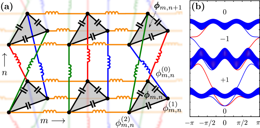
Minimal example.—We distill the idea from Jia et al. in the form of a simplified example (Fig. 1a) and detail how our methods and conclusions apply to Jia et al. elsewhere 11footnotemark: 1. Our circuit consists of a lattice of sites (gray), each site consisting of three nodes. Inductors link sites to each other while capacitors couple the nodes within a site. We stress that no external flux is threaded through any loop of the circuit and the magnetic flux of the Hofstadter model is simulated via the intersite inductive wiring. Transforming the real normal mode frequency matrix into the form of a Hofstadter hopping matrix consists of grouping degrees of freedom into vectors and performing a transformation to complex variables. In an ungrounded circuit, each node (with labeling the degrees of freedom of the site) has a time-integrated absolute voltage associated with it Devoret (1995). This labeling scheme introduces redundant degrees of freedom (which will soon be removed), but allows to be determined analytically. We now group the nodes at each site into a vector . For example, the Lagrangian contribution of the link between site and (see Fig. 1a) is then organized into a (kinetic) capacitive part and a (potential) inductive part
with identity and respective onsite/intersite couplings
| (1) |
Above, the colored matrix elements correspond respectively to the red, blue, and green circuit elements from Fig. 1a, and we have set a uniform capacitance of a third (for normalization) and inductance of one. The equation of motion (EOM) for in the lattice from Fig. 1a is
where and 4 is the number of nearest neighbors for a site in the bulk. The three distinct powers of [] correspond to three vertical inductive wiring permutations and mimic the Hofstadter model in the Landau gauge.
To diagonalize in the index and simultaneously remove the aforementioned redundant degrees of freedom, one can apply a discrete Fourier transform to the three nodes of each site: or ( and repeated indices summed). This site-preserving transformation to a complex vector block-diagonalizes in at the expense of introducing complex numbers. In the basis, the simultaneously diagonal capacitive and inductive coupling matrices are , , and . Since the transformed circuit Lagrangian does not contain terms (since ), the component for each site represents “half” of a degree of freedom (akin to a classical harmonic oscillator in the limit of zero mass) and can be thought of as an ordinary normal mode in the limit of zero capacitance. The EOM for , treated as independent full degrees of freedom (), is
| (3) |
These variables are linear superpositions of bosonic modes and their hopping properties resemble the TRI Hofstadter model in the Landau gauge, i.e., they acquire a (simulated) Peierls phase upon a vertical hopping. Thus, the block-diagonal normal mode frequency matrix consists of the trivial mode matrix and the matrices forming the spin-doubled Hofstadter model.
Topological invariant.—In Fig. 1b, the band structure of () is plotted in red (blue), depicting slightly distorted 22footnotemark: 2 counterpropagating edge modes. Since the pseudo-spin is conserved, the spin-doubled Hofstadter model is characterized by the spin Chern number Sheng et al. (2006) at each gap. Given an edge, the Chern numbers are related to the number of times the edge modes of wind around a horizontal line drawn in the gap (Secs. 5.3.1 and 6.4 in Bernevig and Hughes (2013)). Moreover, the quantity determines whether there is an even or odd number of pairs of counterpropagating edge modes (this is the invariant of the more general TI Kane and Mele (2005b), a QSHI with no spin conservation). The invariant is characterized by Kramers degeneracy, which prohibits elastic backscattering between counterpropagating edge modes only for odd numbers of edge mode pairs per edge Qi and Zhang (2011). Both our example and Jia et al. contain one gapless edge mode pair per edge () and, since pseudo-spin is conserved, constitute a QSHI. Moreover, this system is not a crystalline topological insulator Fu (2011) (as defined in de Leeuw et al. ) since .
Due to the invariants established above, there must exist some operator in the circuit context that mimics the antiunitary electronic time-reversal operator (with and the usual Pauli matrices), squares to , and generates a Kramers degeneracy (a similar observation has been made He et al. with photonic TIs Khanikaev et al. (2013)). Such an operator does indeed exist and comes about from a symmetry of the circuit. In the basis, the coupling matrix , a cyclic permutation of all nodes in each site, commutes with and generates the symmetry group . A generic linear commuting operator (with identity components in the dimensions indexed by ) can be expressed as for some . Since is real, all antilinear extensions of the above operators can be expressed as . In the basis,
which squares to . However, the operator [such that and ] is also in the span of . Thus, electronic time-reversal symmetry in the tight-binding context maps to a combination of ordinary time-reversal and cyclic permutations in the circuit context. We also note that characterizes the conserved pseudo-spin for the time-reversed Hofstadter copies.
Symmetry protection.—Mirroring topological protection in QSHIs and TIs, counterpropagating edge modes of a TI circuit must also be “protected” to some degree. Emulating one-particle elastic scattering processes in TRI electronic systems Qi and Zhang (2011), a crossing between edge modes on the same edge at time-reversal invariant points in the Brillouin zone will not be lifted by inductance or capacitance perturbations that commute with (which is now in the basis). Let a generic inductive link between sites and be parametrized by
| (4) |
where real matrices () are onsite couplings at the two respective sites and is the intersite coupling. Such a perturbation will not cause elastic backscattering between edge modes whenever . For our design, such perturbations are all those which do not break the circuit’s symmetry, i.e., commute with . For example, an identical simultaneous perturbation of all three inductances in any given link [, ] or an onsite perturbation () will not mix edge modes. However, fluctuations of inductance will cause elastic backscattering between edge modes whenever the fluctuations are not identical within any given link. A similar statement holds for capacitive perturbations.
Topologically insulating circuits (i.e., both our design and Jia et al. ) turn out to be similar to certain optical resonator designs Hafezi et al. (2011); *mittal2014 in that both are robust against disorder that does not induce flips of pseudo-spin Lu et al. (2014). In our design, the pseudo-spin is characterized by : since are real matrices, . We also note that, in a realistic setup, both optical resonator edge states and TI circuit edge modes will decay due to optical and microwave dissipation, respectively.
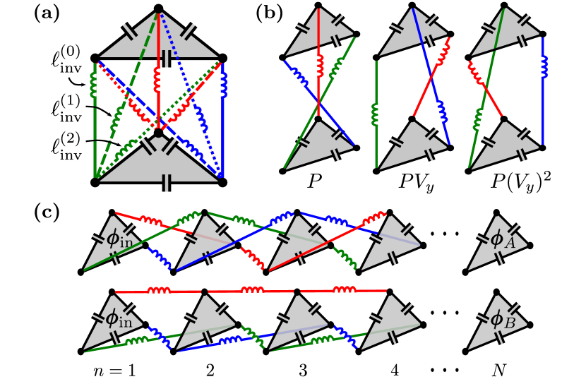
Generalizations.—Given that the above design only has nodes per site, one can consider increasing the number of nodes per site (triangles -gons) and generalizing the cyclic permutation (). This results in a family of models that can emulate TRI Hofstadter hopping matrices with background magnetic flux using nodes per site and vertical connections (with integer ). We note in passing that the case is trivial because it is not gapped in the bulk (see Eq. (5.53) in Bernevig and Hughes (2013)) and that Jia et al. is closely related to 11footnotemark: 1. However, we have developed other generalizations which allow simulation of any background gauge field using circuits that are much more compact. We discuss these approaches below.
First, an arbitrary complex hopping can be achieved using only three nodes per site. For simplicity, we first focus on one link. Instead of having one wiring permutation (e.g. in Fig. 1), one can implement all three permutations in a linear superposition (Fig. 2a). In this case, each permutation gains its own degree of freedom. The intersite inductive coupling matrix is then , where is the inverse inductance of permutation . In the basis, the coupling is diagonal with (no sum over ). Parameterizing the component in terms of an amplitude/phase obtains with
| (5) |
Naturally, and . Additionally, there is a diagonal inductance contribution of to both of the linked sites. Thus, the hopping and diagonal terms can be tuned using with the constraint since . The symmetry protection still holds here since .
Second, non-Abelian couplings can straightforwardly be implemented while still keeping . Instead of using the permutations , three other permutations (with and ; see Fig. 2b) can be superimposed to give an inverse inductance coupling matrix . Nonzero entries of are an off-diagonal hopping and a diagonal contribution . Similar to , the hopping and diagonal terms of can be tuned using . As an example, one can already realize a non-Abelian generalization of the Hofstadter model Osterloh et al. (2005) by letting in Eq. (Topological properties of linear circuit lattices).
The above design allows one to create a lattice with spatially nonuniforn noncommuting unitary hoppings between sites [e.g. using either or ] while maintaining identical onsite contributions (). Despite this flexibility, one cannot create arbitrary hoppings using three nodes per site (assuming onsite contributions are to remain identical). This is because linear superpositions of the six permutations [( and ] with nonnegative real coefficients (since our variables are inverse inductances) do not span all unitary matrices acting on . More permutations are needed, so one needs more nodes per site to generate them. Finding this minimal number of nodes maps to an open problem from group theory Saunders (2008); Elias et al. (2010), and we have determined 11footnotemark: 1 that one needs at most nodes per site to simulate unitary hoppings of dimension .
Non-Abelian Aharonov-Bohm effect.—We finish with a discussion of applications. First we propose an experiment that uses the - duality to observe an electrical non-Abelian Aharonov-Bohm (AB) effect Fang et al. (2013); Osterloh et al. (2005); Jacob et al. (2007). Since all circuit elements are reciprocal here, it is the non-reciprocity of their permutations that leads to interference effects. One can think of as the wavefunctions and sites as spatial positions (Fig. 2c). An incoming signal is applied onto paths and . Let
| (6) |
which is equivalent to . Path contains cyclic permutations from Eq. (1) while path consists of permutations from Fig. 2b (with ). Remembering Eq. (3), we see that a phase of ( is gained by () as the signal “hops” sites in path For path , the and components are exchanged upon each application of . One can superimpose the outputs and to observe their interference. For odd , this interference is constant in time. For even , one should see oscillations due to a nontrivial path :
| (7) |
Since voltage is the derivative of , one can perform the above experiment by applying voltage signals of the form of from Eq. (6), measuring the six output signals at site for paths and , and superimposing them in the manner of Eq. (7). Since the AB effect is nonreciprocal, driving from right to left ( should flip the sign of the phase gained along .
Outlook.—This work generalizes the first realization of a topologically insulating (TI) circuit Jia et al. . We present a simplified circuit whose normal mode frequency matrix is unitarily equivalent to the hopping matrix of the time-reversal invariant Hofstadter model Cocks et al. (2012); *orth2013; *wang2014 with magnetic flux per plaquette. A summary of the equivalence is in Table 1.Since Hofstadter models posses edge modes, we determine which perturbations do not cause edge modes to backscatter.
Additionally, we generalize the approach and determine the minimal circuit complexity required to simulate non-Abelian background gauge fields. Besides a simulation of the Aharonov-Bohm effect, we now speculate on further applications of this circuit QED simulation tool Aspuru-Guzik and Walther (2012); *houck2012; *ashhab2014. A major flexibility is being able to construct and locally probe virtually any lattices (e.g. honeycomb Bermudez et al. (2010) or Kagome Petrescu et al. (2012)) and lattices with connections other than nearest neighbor at the same cost in complexity. Almost any physically relevant and exotic geometry can be implemented Tsomokos et al. (2010) (e.g. a Möbius strip Jia et al. ). One can construct interfaces of lattices and observe mixing of edge modes at the boundary, akin to graphene p-n junctions Abanin and Levitov (2007). To simulate interactions, one can substitute Josephson junctions Girvin (2014) (mechanical oscillators Palomaki et al. (2013); *braginsky) for inductors (capacitors). These and other topics are currently under investigation.
| TRI Hofstadter model | TI circuit |
|---|---|
| Hopping matrix | Normal mode frequency matrix |
| Fermion | with |
| Peierls phase | Intersite wiring permutations |
| Kramers degeneracy | due to symmetry |
Acknowledgements.
We thank J. Simon, D. Schuster, A. Dua, T. Morimoto, B. Elias, W. C. Smith, S. M. Girvin, M. H. Devoret, B. Bradlyn, Z. Minev, and A. Petrescu for fruitful discussions. We thank one of the referees for pointing out the possibility of simulating a magnetic flux of with . This work was supported, in part, by the NSF Graduate Research Fellowship Program under Grant DGE-1122492 (V. V. A.); NSF Grant DMR-1206612 (L. I. G.); and the Army Research Office, Air Force Office of Scientific Research Multidisciplinary Research Program of the University Research Initiative, Defense Advanced Research Projects Agency Quiness program, the Alfred P. Sloan Foundation, and the David and Lucile Packard Foundation (L. J.).References
- Kane and Mele (2005a) C. L. Kane and E. J. Mele, Phys. Rev. Lett. 95, 226801 (2005a).
- Kane and Mele (2005b) C. L. Kane and E. J. Mele, Phys. Rev. Lett. 95, 146802 (2005b).
- Sheng et al. (2005) L. Sheng, D. N. Sheng, C. S. Ting, and F. D. M. Haldane, Phys. Rev. Lett. 95, 136602 (2005).
- Sheng et al. (2006) D. N. Sheng, Z. Y. Weng, L. Sheng, and F. D. M. Haldane, Phys. Rev. Lett. 97, 036808 (2006).
- Bernevig and Zhang (2006) B. A. Bernevig and S.-C. Zhang, Phys. Rev. Lett. 96, 106802 (2006).
- Raghu and Haldane (2008) S. Raghu and F. D. M. Haldane, Phys. Rev. A 78, 033834 (2008).
- Wang et al. (2009) Z. Wang, Y. D. Chong, J. D. Joannopoulos, and M. Soljačić, Nature 461, 772 (2009).
- Koch et al. (2010) J. Koch, A. A. Houck, K. Le Hur, and S. M. Girvin, Phys. Rev. A 82, 043811 (2010).
- Umucalilar and Carusotto (2011) R. O. Umucalilar and I. Carusotto, Phys. Rev. A 84, 043804 (2011).
- Kraus et al. (2012) Y. E. Kraus, Y. Lahini, Z. Ringel, M. Verbin, and O. Zilberberg, Phys. Rev. Lett. 109, 106402 (2012).
- Fang et al. (2012) K. Fang, Z. Yu, and S. Fan, Nat. Photon. 6, 782 (2012).
- Ochiai (2012) T. Ochiai, Phys. Rev. B 86, 075152 (2012).
- Liang and Chong (2013) G. Q. Liang and Y. D. Chong, Phys. Rev. Lett. 110, 203904 (2013).
- Rechtsman et al. (2012) M. C. Rechtsman, J. M. Zeuner, A. Tünnermann, S. Nolte, M. Segev, and A. Szameit, Nat. Photon. 7, 153 (2012).
- Rechtsman et al. (2013) M. C. Rechtsman, J. M. Zeuner, Y. Plotnik, Y. Lumer, D. Podolsky, F. Dreisow, S. Nolte, M. Segev, and A. Szameit, Nature 496, 196 (2013).
- Verbin et al. (2013) M. Verbin, O. Zilberberg, Y. E. Kraus, Y. Lahini, and Y. Silberberg, Phys. Rev. Lett. 110, 076403 (2013).
- Lu et al. (2013) L. Lu, L. Fu, J. D. Joannopoulos, and M. Soljačić, Nat. Photon. 7, 294 (2013).
- Davoyan and Engheta (2013) A. R. Davoyan and N. Engheta, Phys. Rev. Lett. 111, 257401 (2013).
- (19) V. Peano, C. Brendel, M. Schmidt, and F. Marquardt, e-print arXiv:1409.5375 .
- (20) A. V. Nalitov, D. D. Solnyshkov, and G. Malpuech, e-print arXiv:1409.6564 .
- (21) Y.-T. Wang, P.-G. Luan, and S. Zhang, e-print arXiv:1411.2806 .
- (22) T. Karzig, C.-E. Bardyn, N. Lindner, and G. Refael, e-print arXiv:1406.4156 .
- (23) C.-E. Bardyn, T. Karzig, G. Refael, and T. C. H. Liew, e-print arXiv:1409.8282 .
- Hafezi et al. (2011) M. Hafezi, E. A. Demler, M. D. Lukin, and J. M. Taylor, Nat. Phys. 7, 907 (2011).
- Mittal et al. (2014) S. Mittal, J. Fan, S. Faez, A. Migdall, J. M. Taylor, and M. Hafezi, Phys. Rev. Lett. 113, 087403 (2014).
- Khanikaev et al. (2013) A. B. Khanikaev, S. H. Mousavi, W.-K. Tse, M. Kargarian, A. H. MacDonald, and G. Shvets, Nat. Mater. 12, 233 (2013).
- (27) C. He, X.-C. Sun, X.-P. Liu, Z.-W. Liu, Y. Chen, M.-H. Lu, and Y.-F. Chen, e-print arXiv:1401.5603 .
- Lu et al. (2014) L. Lu, J. D. Joannopoulos, and M. Soljačić, Nat. Photon. 8, 821 (2014).
- Yu. Kitaev (2009) A. Yu. Kitaev, AIP Conf. Proc. 1134, 22 (2009).
- Stanescu et al. (2010) T. D. Stanescu, V. Galitski, and S. Das Sarma, Phys. Rev. A 82, 013608 (2010).
- (31) N. Jia, A. Sommer, D. Schuster, and J. Simon, e-print arXiv:1309.0878 .
- Bernevig and Hughes (2013) B. A. Bernevig and T. L. Hughes, Topological Insulators and Topological Superconductors (Princeton University Press, Princeton and Oxford, 2013).
- Azbel (1964) M. Y. Azbel, J. Exp. Theor. Phys. 19, 634 (1964).
- Hofstadter (1976) D. Hofstadter, Phys. Rev. B 14, 2239 (1976).
- Cocks et al. (2012) D. Cocks, P. P. Orth, S. Rachel, M. Buchhold, K. Le Hur, and W. Hofstetter, Phys. Rev. Lett. 109, 205303 (2012).
- Orth et al. (2013) P. P. Orth, D. Cocks, S. Rachel, K. L. Hur, and W. Hofstetter, J. Phys. B: At. Mol. Opt. Phys. 46, 134004 (2013).
- Wang et al. (2014) L. Wang, H.-H. Hung, and M. Troyer, Phys. Rev. B 90, 205111 (2014).
- Haldane (1988) F. D. M. Haldane, Phys. Rev. Lett. 61, 2015 (1988).
- Note (1) See Supplemental Material [URL], which includes Refs. Kibler (2009); Bosma et al. (1997), for a comparison of this work to Jia et al. as well as details on the non-Abelian generalization.
- Kapit (2013) E. Kapit, Phys. Rev. A 87, 062336 (2013).
- Hafezi et al. (2014) M. Hafezi, P. Adhikari, and J. M. Taylor, Phys. Rev. B 90, 060503(R) (2014).
- Gerbier et al. (2013) F. Gerbier, N. Goldman, M. Lewenstein, and K. Sengstock, J. Phys. B: At. Mol. Opt. Phys. 46, 130201 (2013).
- Aidelsburger et al. (2014) M. Aidelsburger, M. Lohse, C. Schweizer, M. Atala, J. T. Barreiro, S. Nascimbène, N. R. Cooper, I. Bloch, and N. Goldman, Nat. Phys. (2014), 10.1038/nphys3171.
- Osterloh et al. (2005) K. Osterloh, M. Baig, L. Santos, P. Zoller, and M. Lewenstein, Phys. Rev. Lett. 95, 010403 (2005).
- Jacob et al. (2007) A. Jacob, P. Ohberg, G. Juzeliunas, and L. Santos, Appl. Phys. B 89, 439 (2007).
- Bermudez et al. (2010) A. Bermudez, N. Goldman, A. Kubasiak, M. Lewenstein, and M. A. Martin-Delgado, New J. Phys. 12, 033041 (2010).
- Note (2) Circuit edge effects distort the original TRI Hofstadter spectrum: the 4 from Eq. (3) is replaced by a 3 (2) for sites on edges (corners). Edge modes exist for all three different types of edges of a vertical strip.
- Devoret (1995) M. H. Devoret, in Quantum Fluctuations, edited by S. Reynaud, E. Giacobino, and J. Zinn-Justin (Elsevier, 1995) Chap. 10.
- Qi and Zhang (2011) X.-L. Qi and S.-C. Zhang, Rev. Mod. Phys. 83, 1057 (2011).
- Fu (2011) L. Fu, Phys. Rev. Lett. 106, 106802 (2011).
- (51) B. de Leeuw, C. Küppersbusch, V. Juricic, and L. Fritz, e-print arXiv:1411.0255 .
- Saunders (2008) N. Saunders, Austral. Math. Soc. Gaz. 35, 332 (2008).
- Elias et al. (2010) B. Elias, L. Silberman, and R. Takloo-Bighash, Experim. Math. 19, 121 (2010).
- Fang et al. (2013) K. Fang, Z. Yu, and S. Fan, Phys. Rev. B 87, 060301 (2013).
- Aspuru-Guzik and Walther (2012) A. Aspuru-Guzik and P. Walther, Nat. Phys. 8, 285 (2012).
- Houck et al. (2012) A. A. Houck, H. E. Tureci, and J. Koch, Nat. Phys. 8, 292 (2012).
- Ashhab (2014) S. Ashhab, New J. Phys. 16, 113006 (2014).
- Petrescu et al. (2012) A. Petrescu, A. A. Houck, and K. Le Hur, Phys. Rev. A 86, 053804 (2012).
- Tsomokos et al. (2010) D. I. Tsomokos, S. Ashhab, and F. Nori, Phys. Rev. A 82, 052311 (2010).
- Abanin and Levitov (2007) D. A. Abanin and L. S. Levitov, Science 317, 641 (2007).
- Girvin (2014) S. M. Girvin, in Quantum Machines: Measurement and Control of Engineered Quantum Systems, edited by M. H. Devoret, B. Huard, R. J. Schoelkopf, and L. F. Cugliandolo (Oxford University Press, Oxford, 2014) Chap. 3.
- Palomaki et al. (2013) T. A. Palomaki, J. W. Harlow, J. D. Teufel, R. W. Simmonds, and K. W. Lehnert, Nature 495, 210 (2013).
- Braginsky and Khalili (1992) V. B. Braginsky and F. Y. Khalili, Quantum Measurement, edited by K. S. Thorne (Cambridge University Press, Cambridge, 1992).
- Kibler (2009) M. R. Kibler, J. Phys. A: Math. Theor. 42, 353001 (2009).
- Bosma et al. (1997) W. Bosma, J. Cannon, and C. Playoust, J. Symbolic Comput. 24, 235 (1997).
χin 1,…,2 See pages χ of tc3_supp.pdf