The nature of domain walls in ultrathin ferromagnets
revealed by scanning nanomagnetometry
The recent observation of current-induced domain wall (DW) motion with large velocity in ultrathin magnetic wires has opened new opportunities for spintronic devices Miron2011 . However, there is still no consensus on the underlying mechanisms of DW motion Miron2011 ; Ryu2013 ; Emori2013 ; Haazen2013 ; Kim2013 ; Garello2013 . Key to this debate is the DW structure, which can be of Bloch or Néel type, and dramatically affects the efficiency of the different proposed mechanisms Thiaville2012 ; Martinez2013 ; Brataas2014 . To date, most experiments aiming to address this question have relied on deducing the DW structure and chirality from its motion under additional in-plane applied fields, which is indirect and involves strong assumptions on its dynamics Ryu2013 ; Emori2013 ; Haazen2013 ; Je2013 . Here we introduce a general method enabling direct, in situ, determination of the DW structure in ultrathin ferromagnets. It relies on local measurements of the stray field distribution above the DW using a scanning nanomagnetometer based on the Nitrogen-Vacancy defect in diamond Taylor2008 ; Gopi2008 ; Rondin2014 . We first apply the method to a Ta/Co40Fe40B20(1 nm)/MgO magnetic wire and find clear signature of pure Bloch DWs. In contrast, we observe left-handed Néel DWs in a Pt/Co(0.6 nm)/AlOx wire, providing direct evidence for the presence of a sizable Dzyaloshinskii-Moriya interaction (DMI) at the Pt/Co interface. This method offers a new path for exploring interfacial DMI in ultrathin ferromagnets and elucidating the physics of DW motion under current.
In wide ultrathin wires with perpendicular magnetic anisotropy (PMA), magnetostatics predicts that the Bloch DW, a helical rotation of the magnetization, is the most stable DW configuration because it minimizes volume magnetic charges Hubert1998 . However, the unexpectedly large velocities of current-driven DW motion recently observed in ultrathin ferromagnets Miron2011 , added to the fact that the motion can be found against the electron flow Ryu2013 ; Emori2013 , has cast doubt on this hypothesis and triggered a major academic debate regarding the underlying mechanism of DW motion Haazen2013 ; Kim2013 ; Garello2013 ; Thiaville2012 ; Martinez2013 ; Brataas2014 . Notably, it was recently proposed that Néel DWs with fixed chirality could be stabilized by the Dzyaloshinskii-Moriya interaction (DMI) Thiaville2012 , an indirect exchange possibly occurring at the interface between a magnetic layer and a heavy metal substrate with large spin-orbit coupling Crepieux1998 . For such chiral DWs, hereafter termed Dzyaloshinskii DWs, a damping-like torque due to spin-orbit terms (spin-Hall effect and Rashba interaction) would lead to efficient current-induced DW motion along a direction fixed by the chirality Thiaville2012 . In order to validate unambiguously these theoretical predictions, a direct, in situ, determination of the DW structure in ultrathin ferromagnets is required. However, the relatively small number of spins at the wall center makes direct imaging of its inner structure a very challenging task. So far, only spin-polarized scanning tunnelling microscopy Meckler2009 and spin-polarized low energy electron microscopy Chen2013 have allowed a direct determination of the DW structure, demonstrating homochiral Néel DWs in Fe double layer on W(110) and in (Co/Ni)n multilayers on Pt or Ir, respectively. However, these techniques are intrinsically limited to model samples due to high experimental constraints and the debate remains open for widely used trilayer systems with PMA such as Pt/Co/AlOx Miron2011 , Pt/Co/Pt Haazen2013 or Ta/CoFeB/MgO Torrejon2013 .
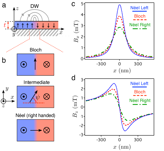
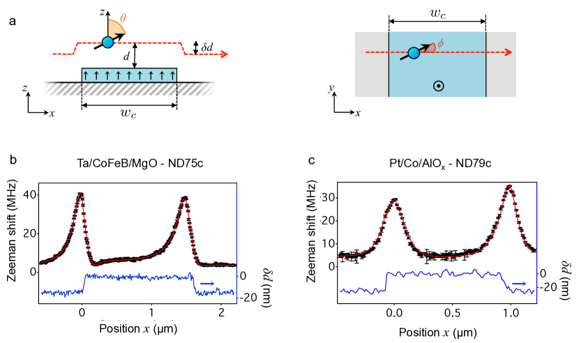
Here we introduce a general method which enables determining the nature of a DW in virtually any ultrathin ferromagnet. It relies on local measurements of the stray magnetic field produced above the DW using a scanning nanomagnetometer. To convey the basic idea behind our method, we start by deriving analytical formulas of the magnetic field distribution at a distance above a DW placed at in a perpendicularly magnetized film [Fig. 1a]. The main contribution to the stray field, denoted , is provided by the abrupt variation of the out-of-plane magnetization Hubert1998 , where is the saturation magnetization and is the DW width parameter. The resulting stray field components can be expressed as
| (1) |
where is the film thickness. These approximate formulas are valid in the limit of (i) , (ii) and (iii) for an infinitely long DW along the axis. On the other hand, the in-plane magnetization, with amplitude , can be oriented with an angle with respect to the axis [Fig. 1b]. This angle is linked to the nature of the DW: for a Bloch DW, whereas or for a Néel DW. The two possible values define the chirality (right or left) of the DW. The spatial variation of the in-plane magnetization adds a contribution to the stray field, whose components are given by
| (2) |
The net stray field above the DW is finally expressed as
| (3) |
which indicates that a Néel DW () produces an additional stray field owing to extra magnetic charges on each side of the wall. Using Eqs. (1) and (2), we find a maximum relative difference in stray field between Bloch and Néel DWs scaling as . Local measurements of the stray field above a DW can therefore reveal its inner structure, characterized by the angle . This is further illustrated in Figs. 1(c,d), which show the stray field components and for various DW configurations while using nm and nm, which are typical parameters of the experiments considered below on a Ta/CoFeB(1nm)/MgO trilayer system.
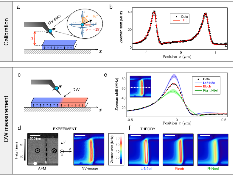
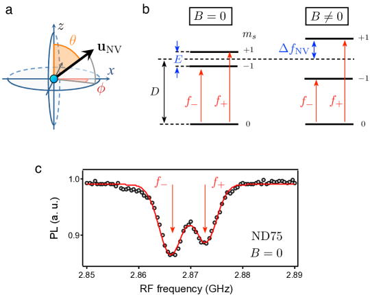
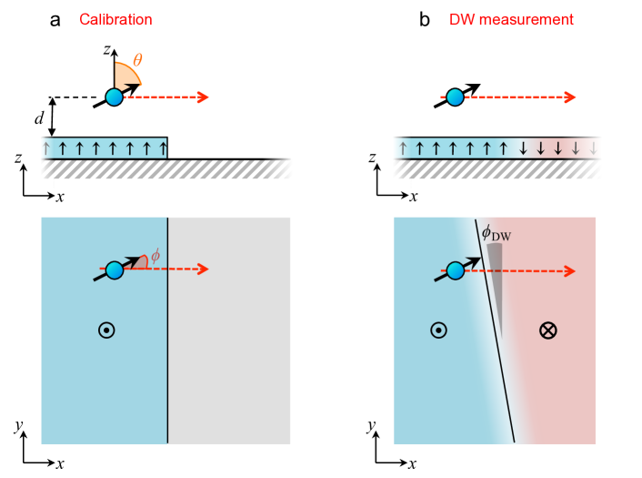
We now demonstrate the effectiveness of the method by employing a single Nitrogen-Vacancy (NV) defect hosted in a diamond nanocrystal as a nanomagnetometer operating under ambient conditions Taylor2008 ; Gopi2008 ; Rondin2014 . Here, the local magnetic field is evaluated within an atomic-size detection volume by monitoring the Zeeman shift of the NV defect electron spin sublevels through optical detection of the magnetic resonance. After grafting the diamond nanocrystal onto the tip of an atomic force microscope (AFM), we obtain a scanning nanomagnetometer which provides quantitative maps of the stray field emanating from nanostructured samples Rondin2013 ; Tetienne2013 ; Tetienne2014 with a magnetic field sensitivity in the range of T.Hz-1/2 Rondin2012 . In this study, the Zeeman frequency shift of the NV spin is measured while scanning the AFM tip in tapping mode, so that the mean distance between the NV spin and the sample surface is kept constant with a typical tip oscillation amplitude of a few nanometers Tetienne2013 . Each recorded value of is a function of and , which are the parallel and perpendicular components, respectively, of the local magnetic field with respect to the NV spin’s quantization axis (Supplementary Section I). Note that a frequently found approximation is , where GHz/T. This indicates that scanning-NV magnetometry essentially measures the projection of the magnetic field along the NV center’s axis. The latter is characterized by spherical angles (,), measured independently in the () reference frame of the sample [Fig. 2a].
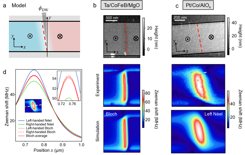
We first applied our method to determine the structure of DWs in a 1.5-m-wide magnetic wire made of a Ta(5 nm)/Co40Fe40B20(1 nm)/MgO(2 nm) trilayer stack (Supplementary Section II). This system has been intensively studied in the last years owing to low damping parameter and depinning field Burrowes2013 . Before imaging a DW, it is first necessary to determine precisely (i) the distance between the NV probe and the magnetic layer and (ii) the product , which are both directly involved in Eq. (3). These parameters are obtained by performing a calibration measurement above the edges of an uniformly magnetized wire, as shown in Fig. 2a. Here we use the fact that the stray field profile above an edge placed at can be easily expressed analytically in a form similar to Eq. (10), which only depends on and . An example of a measurement obtained by scanning the magnetometer across a Ta/CoFeB/MgO stripe is shown in Fig. 2b. The data are fitted with a function corresponding to the Zeeman shift induced by the stray field , where is the width of the stripe (Supplementary Section III-A). Repeating this procedure for a set of independent calibration linecuts, we obtain nm and A, in good agreement with the value measured by other methods Vernier2013 .
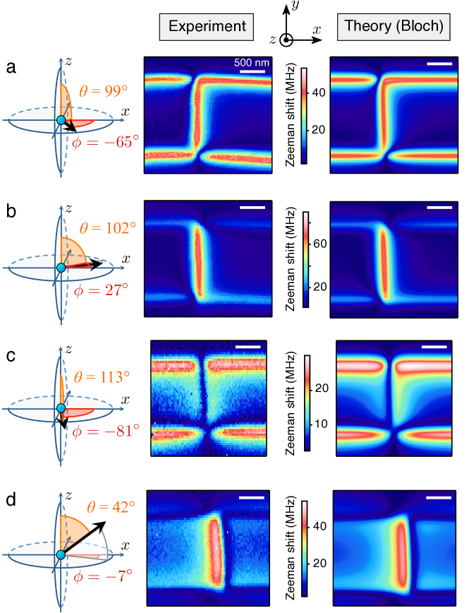
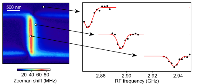
Having determined all needed parameters, it is now possible to measure the stray field above a DW [Fig. 2c] and compare it to the theoretical prediction, which only depends on the angle that characterizes the DW structure. To this end, an isolated DW was nucleated in a wire of the same Ta/CoFeB/MgO film and imaged with the scanning-NV magnetometer under the same conditions as for the calibration measurements. The resulting distribution of the Zeeman shift is shown in Fig. 2d together with the AFM image of the magnetic wire. Within the resolving power of our instrument, limited by the probe-to-sample distance nm Tetienne2013 , the DW appears to be straight with a small tilt angle with respect to the wire long axis, determined to be (Supplementary Section III-B). Taking into account this DW spatial profile, the stray field above the DW was computed for (i) (right-handed Néel DW), (ii) (left-handed Néel DW) and (iii) (Bloch DW). Here we used the micromagnetic OOMMF software oommf ; Rohart2013 rather than the analytical formula described above in order to avoid any approximation in the calculation. The computed magnetic field distributions were finally converted into Zeeman shift distribution taking into account the NV spin’s quantization axis. A linecut of the experimental data across the DW is shown in Fig. 2e, together with the predicted curves in the three above-mentioned cases. Excellent agreement is found if one assumes that the DW is purely of Bloch type. The same conclusion can be drawn by directly comparing the full two-dimensional theoretical maps to the data [Fig. 2d and f]. As described in detail in the Supplementary Section III-C, all sources of uncertainty in the theoretical predictions were carefully analysed, yielding the 1 standard error (s.e.) intervals shown as shaded areas in Fig. 2e. Based on this analysis, we find a 1 s.e. upper limit . This corresponds to an upper limit for the DMI parameter , as defined in Ref. Thiaville2012 , of mJ/m2 (Supplementary Section III-C). This result was confirmed on a second DW in the same wire. In addition, the measurements were reproduced for different projection axes of the NV probe. The results are shown in Fig. 3 for four NV defects with different quantization axes, showing excellent agreement between experiment and theory if one assumes a Bloch-type DW. These experiments provide an unambiguous confirmation of the Bloch nature of the DWs in our sample, but are also a striking illustration of the vector mapping capability offered by NV microscopy, allowing for robust tests of theoretical predictions.
We conclude that there is no evidence for the presence of a sizable interfacial DMI in a Ta(5nm)/Co40Fe40B20(1nm)/MgO trilayer stack. This is in contrast with recent experiments reported on similar samples with different compositions, such as Ta(5nm)/Co80Fe20(0.6nm)/MgO Emori2013 ; Emori2013b and Ta(0.5 nm)/Co20Fe60B20(1nm)/MgO Torrejon2013 , where indirect evidence for Néel DWs was found through current-induced DW motion experiments. We note that contrary to these studies, our method indicates the nature of the DW at rest, in a direct manner, without any assumption on the DW dynamics. Our results therefore motivate a systematic study of the DW structure upon modifications of the composition of the trilayer stack.
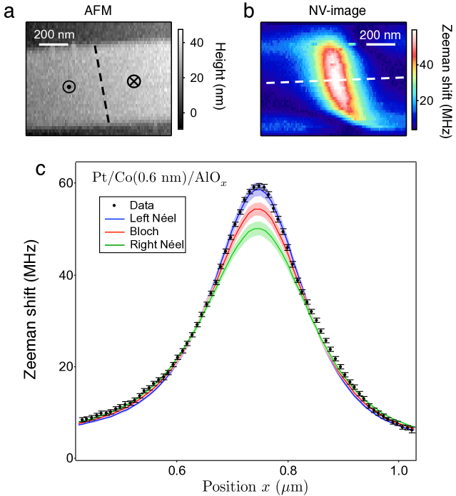
In a second step, we explored another type of sample, namely a Pt(3nm)/Co(0.6 nm)/AlOx(2nm) trilayer grown by sputtering on a thermally oxidized silicon wafer (Supplementary Section II). The observation of current-induced DW motion with unexpectedly large velocities in this asymmetric stack has attracted considerable interest in the recent years Miron2011 . Here, the DW width is nm, leading to a relative field difference between Bloch and Néel cases of at a distance nm. We followed a procedure similar to that described above (Supplementary Section III). After a preliminary calibration of the experiment, a DW in a 500-nm-wide magnetic wire was imaged [Fig. 4a,b] and linecuts across the DW were compared to theoretical predictions [Fig. 4c]. Here the experimental results clearly indicate a Néel-type DW structure with left-handed chirality. The same result was found for two other DWs. This provides direct evidence of a strong DMI at the Pt/Co interface, with a lower bound mJ/m2. This result is consistent with the conclusions of recent field-dependent DW nucleation experiments performed in similar films Pizzini2014 . In addition, we note that the observed left-handed chirality, once combined with a damping-like torque induced by the spin-orbit terms, could explain the characteristics of DW motion under current in this sample Martinez2013 .
In conclusion, we have shown how scanning-NV magnetometry enables direct discrimination between competing DW configurations in ultrathin ferromagnets. This method, which is not sensitive to possible artifacts linked to the DW dynamics, will help clarifying the physics of DW motion under current, a necessary step towards the development of DW-based spintronic devices. In addition, this work opens a new avenue for studying the mechanisms at the origin of interfacial DMI in ultrathin ferromagnets, by measuring the DW structure while tuning the properties of the magnetic material Torrejon2013 ; Ryu2014 . This is a key milestone in the search for systems with large DMI that could sustain magnetic skyrmions Fert2013 .
Aknowledgements. This research has been partially funded by the European Community’s Seventh Framework Programme (FP7/2007-2013) under Grant Agreement n∘ 611143 (Diadems) and n∘ 257707 (Magwire), the French Agence Nationale de la Recherche through the projects Diamag and Esperado, and by C’Nano Ile-de-France (Nanomag).
Author contributions. S.R. and A.T. conceived the idea of the study. J.P.T., T.H., L.J.M. and V.J. performed the experiments, analysed the data and wrote the manuscript. L.H.D, K.G., J.P.A., G.G., L.V., and B.O. prepared the samples. All authors discussed the data and commented on the manuscript.
Supplementary Informations
I Scanning-NV magnetometry
The experimental setup combines a tuning-fork-based atomic force microscope (AFM) and a confocal optical microscope (attoAFM/CFM, Attocube Systems), all operating under ambient conditions. A detailed description of the setup as well as the method to graft a diamond nanocrystal onto the apex of the AFM tip can be found in Ref. [Rondin2012, ].
I.1 Characterization of the magnetic field sensor
The data reported in this work were obtained with NV center magnetometers hosted in three different nanodiamonds, labeled ND74 (data of Figure 3 of the main paper), ND75 (Figure 2) and ND79 (Figure 4). All nanodiamonds were nm in size, as measured by AFM before grafting the nanodiamond onto the AFM tip. The magnetic field was inferred by measuring the Zeeman shift of the electron spin resonance (ESR) of the NV center’s ground state [Rondin2014, ]. This is achieved by monitoring the spin-dependent photoluminescence (PL) intensity of the NV defect while sweeping the frequency of a CW radiofrequency (RF) field generated by an antenna fabricated directly on the sample.
The Hamiltonian used to describe the magnetic-field dependence of the two ESR transitions of this spin system is given by
| (4) |
where and are the zero-field splitting parameters that characterize a given NV center, is the Planck constant, GHz/T [Doherty2012, ], B is the local magnetic field and S is the dimensionless spin operator. Here, the reference frame is defined by the diamond crystal orientation, with being parallel to the NV center’s symmetry axis , as shown in Figure 5(a).
The two ESR frequencies are denoted and and the Zeeman shifts are defined by [Fig. 5(b)]. In general, are functions of and . However, in the limit of small transverse fields () [Tetienne2012, ], they depend only on the magnetic field projection along the NV axis , following the relation
| (5) |
The parameters and were extracted from ESR spectra recorded at zero magnetic field using the fact that [see Fig. 5(b,c)]. In all the data shown in this work, only the upper frequency was measured. Thereafter, we will note the corresponding Zeeman shift , the subscript ‘NV’ reminding that it depends on the direction [Fig. 5(b)]. The experimental measurements of were compared to theory by calculating the expected Zeeman shift through full diagonalization of the Hamiltonian defined by Eq. (4), given the theoretical B map. However, we note that since the condition is usually fulfilled in our measurements, the formula (5) is approximately valid, so that in principle one could retrieve directly the value of with good accuracy ( mT).
The nanodiamonds were recycled several times to be used with different orientations with respect to the reference frame of the sample. The various orientations are labeled with small letters: ND74a, ND74d, ND74e, ND74g, ND75c, ND79c. The spherical angles (,) that characterize the direction were obtained by applying an external magnetic field of known direction and amplitude with a three-axis coil system, following the procedure described in Ref. [Rondin2013, ]. The measurement uncertainty of (standard error) is related to the precision of the calibration of the coils and their alignment with respect to the reference frame.
Table 1 indicates the parameters , , and measured for each NV magnetometer used in this work, with the associated standard errors.
| ND74a | ND74d | ND74e | ND74g | ND75c | ND79c | |
| Figure | 3(a) | 3(b) | 3(c) | 3(d) | 2 | 4 |
| ( MHz) | 2867.1 | 2869.5 | 2866.6 | |||
| ( MHz) | 3.1 | 3.3 | 4.3 | |||
| () | ||||||
| () | ||||||
I.2 Quantitative stray field mapping
The experimental Zeeman shift maps were obtained by recording ESR spectra while scanning the magnetometer with the AFM operated in tapping mode. Each spectrum is composed of 11 bins with a bin size of 2 MHz, leading to a full range of 20 MHz. The integration time per bin is 40 ms, hence 440 ms per spectrum, that is, 440 ms per pixel of the image. As illustrated in Figure 6, only the upper frequency is probed, and the measurement window is shifted from pixel to pixel in order to track the resonance. Each spectrum is then fitted with a Gaussian lineshape to obtain and thus . The full width at half maximum (FWHM) is typically 5-10 MHz, and the standard error on is MHz with the above-mentioned acquisition parameters.
II Samples
Two samples, Ta/CoFeB/MgO and Pt/Co/AlOx, were investigated in this work. The Ta/CoFeB/MgO trilayer was deposited on a Si/SiO2(100 nm) wafer using a PVD Timaris deposition tool by Singulus Tech. The film stack composition is Ta(5)/CoFeB(1)/MgO(2)/Ta(5), starting from the SiO2 layer (units in nanometer). The stoichiometric composition of the as-deposited magnetic layer is Co40Fe40B20. The second sample was fabricated from Pt(3)/Co(0.6)/Al(1.6) layers deposited on a thermally oxidized silicon wafer by d.c. magnetron sputtering. After deposition, the aliminium layer was oxidized by exposure to an oxygen plasma. Both samples were patterned using e-beam lithography and ion milling. A second step of e-beam lithography was finally performed in order to define a gold stripline for RF excitation, which is used to record the Zeeman shift of the NV defect magnetometer [cf. section I.1].
Figure 7 shows the general schematic of the samples, highlighting the regions used for calibration linecuts (stripe of width ) and DW measurements (stripe of width ) [cf. section III.1]. The use of two perpendicular wires ensures that the DW is approximately parallel to the edges used for calibration. The final dimensions (height , widths and ) of the patterned structures were measured with a calibrated AFM. For the Ta/CoFeB/MgO sample, nm and nm, whereas for the Pt/Co/AlOx sample nm, nm and nm. The nucleation was achieved by feeding a current pulse through the gold stripline for the Ta/CoFeB/MgO sample, and by applying pulses of out-of-plane magnetic field for the Pt/Co/AlOx sample.
III Data analysis
III.1 Calibration linecuts
III.1.1 Fit procedure
As discussed in the main text, a preliminary calibration of the experiment is required in order to infer the probe-sample distance and the saturation magnetization of the sample . This calibration is performed by measuring the Zeeman shift of the NV magnetometer while scanning it across a stripe of the ferromagnetic layer in the direction, as depicted in Figure 8(a). Since is of the order of 100 nm in our experiments, one has where is the thickness of the magnetic layer, so that the edges can be considered to be abrupt, i.e. and otherwise, with the stripe width. In fact, due to the topography of the sample, the effective distance between the NV spin and the magnetic layer varies during the scan [see Fig. 8(a)]. This position-dependent distance can be written as , where on average when the tip is above the stripe, and on average when the tip is above the bare substrate. Here is the total height of the patterned structures [cf. Section II]. Experimentally, one has access to the relative variations of thanks to the simultaneously recorded AFM topography information, hence one can infer the function . Therefore, only the absolute distance, characterized by , is unknown.
The stray field components above a single abrupt edge parallel to the direction, positioned at (magnetization pointing upward for ), are given by
| (6) |
These formulas correspond to the thin-film limit () of exact formulas, but the relative error introduced by the approximation is in our case (), which is negligible compared with other sources of error (see below). The field above a stripe is then obtained by simply adding the contribution of the two edges, namely
| (7) |
Using Eqs. (6) and (7), we obtain an analytical formula for the stray field above the stripe. A fit function is then obtained by converting the field distribution into Zeeman shift of the NV defect after diagonalization of the Hamiltonian defined by Eq. (4), with the characteristic parameters () of the NV magnetometer. The fit parameters are the maximum distance and the product . The geometric parameters of the stripe (width and height ), measured independently, serve as references to rescale the length scales and in the linecut data before fitting. Note that in assuming an uniformely magnetized stripe, we neglect the rotation of the magnetization near the edges induced by the Dzyaloshinskii-Moriya interaction (DMI) [Rohart2013, ]. The effect of this rotation will be discussed in Section III.4.
In the following, we focus on the experiments performed (i) with ND75c on the Ta/CoFeB/MgO sample and (ii) with ND79c on the Pt/Co/AlOx sample, corresponding to the experimental results reported in Figures 2 and 4 of the main paper, respectively. Typical calibration linecuts are shown in Figures 8(b,c) together with the topography of the sample. The red solid line is the result of the fit, showing a very good agreement with the experimental data.
III.1.2 Uncertainties
Uncertainties on the fit parameters come from those on (i) the NV center’s parameters , (ii) the geometric parameters of the stripe () and (iii) the fit procedure. There are therefore six independent parameters which introduce uncertainties on the outcome of the fit. In the following, these parameters are denoted as where is the nominal value of parameter and its standard error. The uncertainties on , , and (resp. on and ) are discussed in Section I.1 (resp. in Section II). The nominal values and the standard errors on each parameter are summarized in Table 2.
The uncertainty and reproducibility of the fit procedure were first analyzed by fitting independent calibration linecuts while fixing the parameters to their nominal values . As an example, the histograms of the fit outcomes for are shown in Figure 9(a,b) for a set of 13 calibration linecuts recorded on the Ta/CoFeB/MgO sample with ND75c. From this statistic, we obtain A and nm. Here the error bar is given by the standard deviation of the statistic. The relative uncertainty of the fit procedure is therefore given by for the probe-sample distance and for the product .
We now estimate the relative uncertainty on the fit outcomes linked to each independent parameter . For that purpose, the set of calibration linecuts was fitted with one parameter fixed at , all the other five parameters remaining fixed at their nominal values. The resulting mean values of the fit parameters are denoted and and the relative uncertainty introduced by the errors on parameter is finally defined as
| (8) |
To illustrate the method, we plot in Figure 9(c,d) the histograms of the fit outcomes while changing the zero-field splitting parameter from to . For this parameter, the relative uncertainties on and are and . The same analysis was performed for all parameters and the corresponding uncertainties are summarized in Table 2. The cumulative uncertainty is finally given by
| (9) |
where all errors are assumed to be independent.
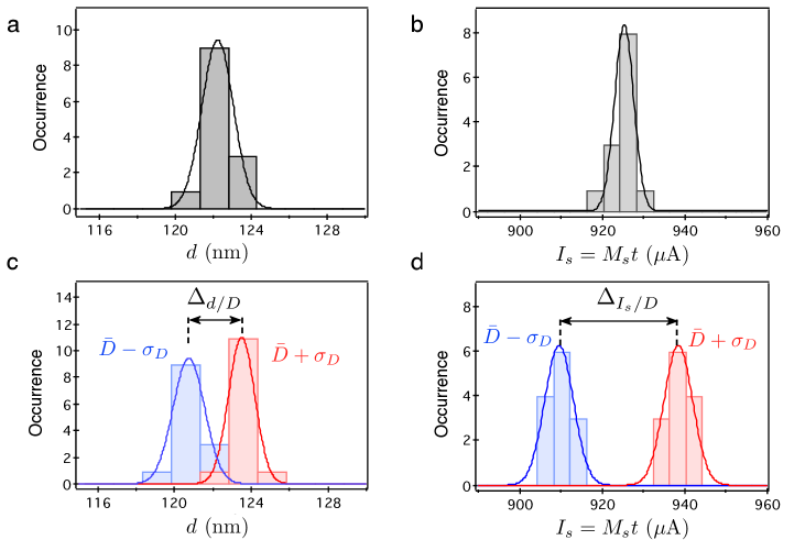
Following this procedure, we finally obtain nm and A (or MA/m) for the Ta/CoFeB/MgO sample, and nm and A (or MA/m) for the Pt/Co/AlOx sample, in good agreement with the values reported elsewhere for similar samples [Vernier2014, ; Miron2010, ].
(a) Ta/CoFeB/MgO with ND75c
parameter
nominal value
uncertainty
1500 nm
30 nm
1.8
2.0
nm
nm
1.0
0.2
0.9
0.7
0.2
1.2
MHz
MHz
1.0
1.6
MHz
MHz
0.5
0.5
2.5
2.9
(b) Pt/Co/AlOx with ND79c
parameter
nominal value
uncertainty
980 nm
20 nm
1.8
2.0
nm
nm
1.6
0.4
0.2
0.1
1.4
MHz
MHz
0.8
0.8
MHz
MHz
2.9
2.6
III.2 Micromagnetic calculations
While the calibration linecuts were fitted with analytic formulas, the predictions of the stray field above the DWs were obtained using micromagnetic calculations in order to accurately describe the DW fine structure. We first used the micromagnetic OOMMF software [oommf, ; Rohart2013, ] to obtain the equilibrium magnetization of the structure. For the Ta/CoFeB/MgO sample, the nominal values used in OOMMF are: anisotropy constant J/m3 (obtained from the measured effective anisotropy field of 107 mT [Devolder2013, ]), exchange constant pJ/m, film thickness nm, stripe width nm, cell size nm3. For the Pt/Co/AlOx sample, we used: J/m3 (measured effective anisotropy field of 920 mT), pJ/m, nm, nm, cell size nm3. The saturation magnetization was obtained from the product determined from calibration linecuts [cf. Section III.1].
We considered a straight DW with a tilt angle with respect to the axis [Fig. 10(a)]. As illustrated in Figs. 10(b) and 10(c), this angle was directly inferred from the Zeeman shift images, leading to for the DW studied in Fig. 2 of the main paper, and for the DW studied in Fig. 4 of the main paper. The uncertainty on enables us to account for the fact that the DW is not necessarily rigorously straight. This point will be discussed in Section III.3.
The calculation of the stray field was then performed with four different initializations of the DW magnetization: (i) right-handed Bloch, (ii) left-handed Bloch, (iii) right-handed Néel and (iv) left-handed Néel. To stabilize the Néel configuration, the DMI at one of the interfaces of the ferromagnet was added, as described in Ref. [Rohart2013, ]. The value of the DMI parameter was set to mJ/m2, which is large enough to fully stabilize a Néel DW. The additional consequences of a stronger DMI will be discussed in Section III.4.
Once the equilibrium magnetization was obtained, the stray field distribution was calculated at the distance by summing the contribution of all cells. Knowing the projection axis (,), we finally calculate the Zeeman shift map by diagonalizing the NV center’s Hamiltonian [cf. Section I.1]. Under the conditions of Figs. 2 and 4 of the main paper, the difference of stray field near the maximum between left-handed and right-handed Bloch DWs is predicted to be [Fig. 10(d)]. Since this is much smaller than the standard error [cf. Section III.3], we plotted the mean of these two cases, which is simply referred to as a Bloch DW, and added the deviation induced by the two possible chiralities to the displayed standard error.
III.3 Uncertainties on the DW stray field predictions
In this Section, we analyze how the uncertainties on the preliminary measurements affect the final predictions of the Zeeman shift above the DW. To keep the analysis simple and insightful, we use the approximate analytic expressions of the stray field of an infinitely long DW [Eqs. (1), (2) and (3) of the main paper]. Furthermore, we focus our attention on the positions where the DW stray field is maximum, since this is what provides information about the DW nature [see Figs. 1(c) and 1(d) of the main paper]. Finally, we use the approximation [cf. Section I.1], which is quite accurate near the stray field maximum and allows us to consider the magnetic field rather than the Zeeman shift . For clarity the subscript will be dropped and the projected field will be simply denoted .
III.3.1 Out-of-plane contribution
Let us first consider the out-of-plane contribution to the DW stray field, . The stray field components above the DW can be written, in the axis system (Fig. 11), as
| (10) |
where is the position of the DW (for a given ). This is simply twice the stray field above an edge [see Eq. (6)] expressed in a rotated coordinate system. The projection along the NV center’s axis is
| (11) | |||||
| (12) |
We now link to the calibration measurement. For simplicity, we consider only one of the two edges of the calibration stripe, e.g. the edge at . We can thus write the projected field above the edge, at a distance , as
| (13) | |||||
| (14) |
Comparing Eqs. (12) and (14), one finds the relation
| (15) |
where we define
| (16) |
Since is experimentally measured, in principle one can use Eq. (15) to predict by simply evaluating the function as defined by Eq. (16). As implies , it comes that, in a first approximation, can be obtained without the need for precise knowledge of any parameter. In other words, the calibration measurement, performed under the same conditions as for the DW measurement, allows us to accurately predict the DW field even though those conditions are not precisely known. This is the key point of our analysis.
Strictly speaking, , hence , does depend on some parameters as soon as , namely on . To get an insight into how important the knowledge of is, we need to examine how sensitive is with respect to errors on . Owing to the sine and cosine functions in Eq. (16), the smallest sensitivity to parameter variations (vanishing partial derivatives) is achieved when either (i) (projection axis perpendicular to the sample plane) or (ii) (projection axis parallel to the sample plane) combined with and . However, case (i) cannot be achieved in our experiment, because the out-of-plane RF field cannot efficiently drive ESR of a spin pointing out-of-plane. We therefore target case (ii), that is, and . For that purpose, we use a calibration edge that is as parallel to the DW as possible () and we seek to have a projection axis that is as perpendicular to the DW plane as possible ( and ). This is why we employ two perpendicular wires for the calibration and the DW measurements, respectively [cf. Section II]. Conversely, in the worst case of (calibration edge perpendicular to the DW) with , one would have , directly proportional to the errors on and .
To be more quantitative, we use Eq. (15) to express the uncertainty on the prediction as a function of the uncertainties on the various quantities, which gives
| (17) |
Here, is given by the measurement error of , whereas is the uncertainty on introduced by the error on the parameter , the other parameters being fixed at their nominal values, as defined by
| (18) |
The results are summarized in Table 3 for the cases considered in Figs. 2 (Ta/CoFeB/MgO sample) and 4 (Pt/Co/AlOx sample) of the main paper. is evaluated for , which is the position where the field is maximum. It can be seen that the dominating source of uncertainty, though small (), is the error on , while the errors on , and have a negligible impact.
In practice, to obtain the theoretical predictions shown in the main paper and in Fig. 10, we do not use explicitly Eq. (15), but rather use the set of parameters determined following the calibration step, and put it into the stray field computation [cf. Section III.2]. This allows us to simulate more complex structures than the idealized infinitely long DW considered above [Fig. 11(b)], in particular the finite-width wires studied in this work. However, we stress that, as far as the uncertainties are concerned, this is completely equivalent to using Eq. (15), since is fully characterized by the set [cf. Section III.1]. The main difference comes from the influence of the edges of the wire, of width , on the DW stray field. The standard error then translates into a relative error on the DW field . For the Ta/CoFeB/MgO sample, nm, which gives a negligible error for the field calculated at the center of the stripe. For the Pt/Co/AlOx sample, the stripe is narrower, nm, leading to . The overall uncertainty on the prediction , for a DW confined in a wire, then becomes
| (19) |
The overall errors are indicated in Table 3. For Ta/CoFeB/MgO (Fig. 2 of the main paper ), the overall standard error is found to be , whereas for Pt/Co/AlOx (Fig. 4) it is , in both cases much smaller than the difference between Bloch and Néel DW configurations.
(a) Ta/CoFeB/MgO with ND75c
parameter
nominal value
uncertainty
nm
nm
0.2
1.1
1.5
(b) Pt/Co/AlOx with ND79c
parameter
nominal value
uncertainty
nm
nm
0.4
1.1
2.1
III.3.2 In-plane contribution
According to Eq. (2) of the main paper, the in-plane contribution to the DW stray field, , is proportional to and to the DW width , where is the exchange constant and the effective anisotropy constant. The values of reported in the literature for Co and CoFeB thin films range from 10 to 30 pJ/m (see e.g. Refs. [Yamanouchi2011, ; Eyrich2012, ]). Based on this range, we deduced a range for , namely 15-25 nm for the Ta/CoFeB/MgO sample and 4.4-7.6 nm for the Pt/Co/AlOx sample. This amounts to a relative variation around the mid-value of . Thus, is dominated by the uncertainty on the DW width, that is, . All other errors can be neglected in comparison. In the simulations [cf. Section III.2], we used the value of that gives the mid-value of , that is pJ/m for Ta/CoFeB/MgO ( nm) and pJ/m for Pt/Co/AlOx ( nm).
For an arbitrary angle of the in-plane magnetization of the DW, the projected stray field writes
| (20) |
where it is assumed that . We deduce the expression of the absolute uncertainty for
| (21) |
where and . This is how the confidence intervals shown in Figs. 2 and 4 of the main paper were obtained. Finally, the confidence intervals for were defined as the values of such that the data points remain in the interval . The interval for the DMI parameter was deduced using the relation [Thiaville2012, ]
| (22) |
which holds for an up-down DW provided that .
III.4 Effects of a large DMI constant
So far, we have only considered, for simplicity and to avoid introducing additional parameters, the effect of DMI on the angle of the in-plane DW magnetization. In doing so, two other effects of DMI have been neglected: (i) the DMI induces a rotation of the magnetization near the edges of the ferromagnetic structure [Rohart2013, ] and (ii) the DW profile in the presence of DMI slightly deviates from the profile [Thiaville2012, ]. The first (second) effect modifies the stray field above the calibration stripe (above the DW). Here we quantify these effects for the case of Pt/Co/AlOx, for which the DMI is expected to be strong.
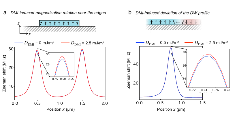
Recently, Martinez et al. have estimated that a value mJ/m2 associated with the spin Hall effect would quantitatively reproduce current-induced DW velocity measurements in Pt/Co/AlOx [Martinez2013, ]. On the other hand, Pizzini et al. have inferred a similar value of mJ/m2 from field-dependent DW nucleation experiments [Pizzini2014, ]. This is of the threshold value above which the DW energy becomes negative and a spin spiral develops. Taking mJ/m2, we predict that the magnetization rotation at the edges reaches [Rohart2013, ]. As a result, the field maximum above the edge is increased by , under the conditions of Fig. 8(b) [Fig. 12(a)]. This is of the order of our measurement error, so that this DMI-induced magnetization rotation cannot be directly detected in our experiment. In fitting the data of Fig. 8(b), the outcome for and is changed by a similar amount: we found nm and A without DMI, as compared with nm and A if mJ/m2 is included. The difference is below the uncertainty, therefore it does not affect the interpretation of the data measured above the DW.
To quantify the second effect, we performed the OOMMF calculation with two different values of that stabilize a left-handed Néel DW: mJ/m2, as used for the simulations shown in the main paper, and mJ/m2. The stray field calculations, under the same conditions as in Fig. 4 of the main paper, show an increase of the field maximum by for the stronger DMI [Fig. 12(b)]. Again, this is well below the uncertainty [cf. Section III.3].
Besides, it is worth pointing out that these two effects tend to compensate each other, since the first one tends to increase the estimated distance , thereby decreasing the predicted DW field, while the second one tends instead to increase the predicted DW field. Overall, we conclude that neglecting the additional effects of DMI provides predictions for the Néel DW stray field that are correct within the uncertainty, even with a DMI constant as large as of . We note finally that the predictions for the Bloch case, as plotted in Fig. 2 and 4 of the main paper, are anyway not affected by the above considerations, since the Bloch case implies no DMI at all.
References
- (1) I. M. Miron et al., Fast current-induced domain-wall motion controlled by the Rashba effect, Nat. Mater. 10, 419 (2011).
- (2) K.-S. Ryu, L. Thomas, S.-H. Yang, and S. Parkin, Chiral spin torque at magnetic domain walls, Nat. Nano. 8, 527 (2013).
- (3) S. Emori, U. Bauer, S.-M. Ahn, E. Martinez, and G. S. D. Beach, Current-driven dynamics of chiral ferromagnetic domain walls, Nat. Mater. 12, 611 (2013).
- (4) P. P. J. Haazen, E. Murè, J. H. Franken, R. Lavrijsen, H. J. M. Swagten, and B. Koopmans, Domain wall depinning governed by the spin Hall effect, Nat. Mater. 12, 299 (2013).
- (5) J. Kim, J. Sinha, M. Hayashi, M. Yamanouchi, S. Fukami, T. Suzuki, S. Mitani, and H. Ohno, Layer thickness dependence of the current-induced effective field vector in Ta/CoFeB/MgO, Nat. Mater. 12, 240 (2013).
- (6) K. Garello, I. M. Miron, C. O. Avci, F. Freimuth, Y. Mokrousov, S. Blgel, S. Auffret, O. Boulle, G. Gaudin, and P. Gambardella, Symmetry and magnitude of spin-orbit torques in ferromagnetic heterostructures, Nat. Nanotech. 8, 587 (2013).
- (7) A. Thiaville, S. Rohart, E. Jué, V. Cros, and A. Fert, Dynamics of Dzyaloshinskii domain walls in ultrathin magnetic films, Europhys. Lett. 100, 57002 (2012).
- (8) E. Martinez, S. Emori, and G. S. D. Beach, Current-driven domain wall motion along high perpendicular anisotropy multilayers: The role of the Rashba field, the spin Hall effect, and the Dzyaloshinskii-Moriya interaction, Appl. Phys. Lett. 103, 072406 (2013).
- (9) A. Brataas, and K. M. D. Hals, Spin-orbit torques in action, Nat. Nano. 9, 86 (2014).
- (10) S.-G. Je, D.-H. Kim, S.-C. Yoo, B.-C. Min, K.-J. Lee, and S.-B. Choe, Asymmetric magnetic domain-wall motion by the Dzyaloshinskii-Moriya interaction, Phys. Rev. B 88, 214401 (2013).
- (11) J. M. Taylor et al., High-sensitivity diamond magnetometer with nanoscale resolution. Nat. Phys. 4, 810 (2008).
- (12) G. Balasubramanian et al., Nanoscale imaging magnetometry with diamond spins under ambient conditions. Nature 455, 648 (2008).
- (13) L. Rondin, J.-P. Tetienne, T. Hingant, J.-F. Roch, P. Maletinsky, and V. Jacques, Magnetometry with nitrogen-vacancy defects in diamond. Rep. Prog. Phys. 77, 056503 (2014).
- (14) A. Hubert, and R. Schäfer, Magnetic domains (Springer Verlag, Berlin) 1998.
- (15) A. Crépieux, and C. Lacroix, Dzyaloshinsky-Moriya interactions induced by symmetry breaking at a surface, J. Magn. Magn. Mater. 182, 341 (1998).
- (16) S. Meckler et al., Real-space observation of a right-rotating inhomogeneous cycloidal spin spiral by spin-polarized scanning tunneling microscopy in a triple axes vector magnet, Phys. Rev. Lett. 103, 157201 (2009).
- (17) G. Chen, T. Ma, A. T. N’Diaye, H. Kwon, C. Won, Y. Wu, and A. K. Schmid, Tailoring the chirality of magnetic domain walls by interface engineering, Nat. Commun. 4, 2671 (2013).
- (18) J. Torrejon, J. Kim, J. Sinha, S. Mitani, M. Hayashi, M. Yamanouchi, and H. Ohno, Interface control of the magnetic chirality in CoFeB/MgO heterostructures with heavy metal underlayers, preprint arXiv:1401.3568 (2013).
- (19) L. Rondin et al., Stray-field imaging of magnetic vortices with a single diamond spin, Nat. Commun. 4, 2279 (2013).
- (20) J.-P. Tetienne et al., Quantitative stray field imaging of a magnetic vortex core, Phys. Rev. B 88, 214408 (2013).
- (21) J.-P. Tetienne, T. Hingant, J.-V. Kim, L. Herrera Diez, J.-P. Adam, K. Garcia, J.-F. Roch, S. Rohart, A. Thiaville, D. Ravelosona, V. Jacques, Nanoscale imaging and control of domain-wall hopping with a nitrogen-vacancy center microscope, Science 344, 1366 (2014).
- (22) L. Rondin et al., Nanoscale magnetic field mapping with a single spin scanning probe magnetometer, Appl. Phys. Lett. 100, 153118 (2012).
- (23) C. Burrowes et al., Low depinning fields in Ta-CoFeB-MgO ultrathin films with perpendicular magnetic anisotropy, Appl. Phys. Lett. 103, 182401 (2013).
- (24) N. Vernier, J.P. Adam, S.Eimer, G. Agnus, T. Devolder, T. Hauet, B. Ockert, and D. Ravelosona, Measurement of magnetization using domain compressibility in CoFeB films with perpendicular anisotropy, Appl. Phys. Lett. 104, 122404 (2014).
- (25) M. J. Donahue, and D. G. Porter, OOMMF User’s Guide, Version 1.0 Interagency Report NISTIR 6376, National Institute of Standards and Technology, Gaithersburg, MD. http://math.nist.gov/oommf (1999).
- (26) S. Rohart and A. Thiaville, Skyrmion confinement in ultrathin film nanostructures in the presence of Dzyaloshinskii-Moriya interaction, Phys. Rev. B 88, 184422 (2013).
- (27) S. Emori, E. Martinez, U. Bauer, S.-M. Ahn, P. Agrawal, D. C. Bono, G. S. D. Beach, Spin Hall torque magnetometry of Dzyaloshinskii domain walls, preprint arXiv:1308.1432 (2013).
- (28) S. Pizzini, J. Vogel, S. Rohart, L. D. Buda-Prejbeanu, E. Jué, O. Boulle, I. M. Miron, C. K. Safeer, S. Auret, G. Gaudin and A. Thiaville, Chirality-induced asymmetric magnetic nucleation in Pt/Co/AlOx ultrathin microstructures, preprint arXiv:1403.4694 (2014).
- (29) K.-S. Ryu, S.-H. Yang, L. Thomas, and S. S. P. Parkin, Chiral spin torque arising from proximity-induced magnetization, Nat. Commun. 5, 3910 (2014).
- (30) A. Fert, V. Cros, J. Sampaio, Skyrmions on the track, Nat. Nano. 8, 152 (2013).
- (31) M. W. Doherty, F. Dolde, H. Fedder, F. Jelezko, J. Wrachtrup, N. B. Manson, L. C. L. Hollenberg, Theory of the ground-state spin of the NV- center in diamond, Phys. Rev. B 85, 205203 (2012).
- (32) J.-P. Tetienne et al., Magnetic-field-dependent photodynamics of single NV defects in diamond: an application to qualitative all-optical magnetic imaging. New J. Phys. 14, 103033 (2012).
- (33) T. Devolder et al., Damping of CoxFe80-xB20 ultrathin films with perpendicular magnetic anisotropy. Appl. Phys. Lett. 102, 022407 (2013).
- (34) N. Vernier et al., Measurement of magnetization using domain compressibility in CoFeB films with perpendicular anisotropy. Appl. Phys. Lett. 104, 122404 (2014).
- (35) I. M. Miron et al., Current-driven spin torque induced by the Rashba effect in a ferromagnetic metal layer. Nat Mater. 9, 230 (2010).
- (36) M. Yamanouchi et al., Domain structure in CoFeB thin films with perpendicular magnetic anisotropy. IEEE Magn. Lett. 2, 3000304 (2011).
- (37) C. Eyrich , Exchange Stiffness in Thin-Film Cobalt Alloys. MSc Thesis (2012, Simon Fraser University, Canada).