Directional and dynamic modulation of the optical emission of an individual \ceGaAs nanowire using surface acoustic waves
Abstract
We report on optical experiments performed on individual nanowires and the manipulation of their temporal emission characteristics using a surface acoustic wave. We find a pronounced, characteristic suppression of the emission intensity for the surface acoustic wave propagation aligned with the axis of the nanowire. Furthermore, we demonstrate that this quenching is dynamical as it shows a pronounced modulation as the local phase of the surface acoustic wave is tuned. These effects are strongly reduced for a SAW applied in the direction perpendicular to the axis of the nanowire due to their inherent one-dimensional geometry. We resolve a fully dynamic modulation of the nanowire emission up to MHz not limited by the physical properties of the nanowires.
keywords:
Surface acoustic waves, nanowires, photoluminescence, acoustoelectric effectsUniv. Augsburg]Lehrstuhl für Experimentalphysik 1 and Augsburg Centre for Innovative Technologies (ACIT), Universität Augsburg, Universitätsstr. 1, 86159 Augsburg, Germany TU München]Walter Schottky Institut and Physik Department, Technische Universität München, Am Coulombwall, 85748 Garching, Germany TU München]Walter Schottky Institut and Physik Department, Technische Universität München, Am Coulombwall, 85748 Garching, Germany TU München]Walter Schottky Institut and Physik Department, Technische Universität München, Am Coulombwall, 85748 Garching, Germany TU München]Walter Schottky Institut and Physik Department, Technische Universität München, Am Coulombwall, 85748 Garching, Germany TU München]Walter Schottky Institut and Physik Department, Technische Universität München, Am Coulombwall, 85748 Garching, Germany Univ. Augsburg]Lehrstuhl für Experimentalphysik 1 and Augsburg Centre for Innovative Technologies (ACIT), Universität Augsburg, Universitätsstr. 1, 86159 Augsburg, Germany Univ. Augsburg]Lehrstuhl für Experimentalphysik 1 and Augsburg Centre for Innovative Technologies (ACIT), Universität Augsburg, Universitätsstr. 1, 86159 Augsburg, Germany
Semiconductor nanowires (NWs) offer a particularly promising platform to combine both electrostatic 1, *Fasth:05a, *Pfund:06 and optically active heterostructure quantum dots (QDs) 4, *Weert:09a, *Kouwen:10a in an inherently scalable architecture for the implementation of electro-optical 7, *Hanson:07 spin-based quantum information schemes. Furthermore, these types of nanostructures allow for confinement of both electronic and photonic degrees of freedom9 providing a direct interconnect between localized spin and flying photonic qubits. To fully exploit the advantages of isolated electron spins in electrostatic QDs and their conversion into photons in a heterostructure QD on the same NW a non-invasive, fast bus is required. This bus could be implemented using spin-preserving acoustoelectric charge conveyance10, *Stotz:05 mediated by high-frequency surface acoustic waves (SAWs). SAWs have a long-standing history as a versatile tool to dynamically control and manipulate embedded optically active nanosystems such as quantum wells 12, quantum wires 13 and quantum dots 14, *Metcalfe:10 and columnar quantum posts 16 with frequencies ranging from tens of MHz up to several GHz. In these experiments acoustic charge conveyance of charges, spins and dissociated excitons, inherently sequential electron-hole injection and modulation of the emission wavelength of these planar semiconductor heterostructures have been observed. In contrast, reports on SAW control of isolated one-dimensional nanosystems such as nanotubes and NWs are so far limited to electric transport experiments 17, *Roddaro:10 in which only one carrier species is probed.
Here we demonstrate dynamic control of the emission of single \ceGaAs NWs employing high frequency SAWs. We find a pronounced directionality of this process as its efficiency is strongly enhanced for SAWs propagating along the NW axis. This observation is in excellent agreement with a dissociation process of photogenarated electron-hole pairs by the piezoelectric fields generated by the SAW. This process is inhibited for SAWs propagating perpendicular to the NW axis since their diameter is more than one order of magnitude smaller than the wavelength of the SAW. This is in strong contrast to embedded low-dimensional semiconductor nanostructures which are typically surrounded and coupled to systems of higher dimensionality (quantum wells and bulk).
The NWs studied were fabricated by molecular beam epitaxy (MBE) using an autocatalytic growth process on Si (111) substrates covered by
an ultra-thin amorphous nucleation mask 19, *Koblmueller:10a. These NWs have typical lengths
of and diameters of nm with predominantly zinc blende crystal structure
as confirmed by X-ray diffraction, transmission electron microscopy and Raman spectroscopy 21. We prepared
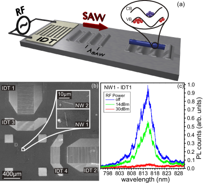
a hybrid SAW device to study individual NWs, a schematic and a scanning electron micrograph (SEM) of which is shown in 1 (a) and (b), respectively. First, we realize a SAW chip by defining interdigital transducers (IDTs) labeled IDT1–IDT4 on a XY-cut substrate using electron beam
lithography and a lift-of process. The periodicities chosen for IDT1/IDT2 and IDT3/IDT4 allow for the excitation of SAWs of wavelengths and , respectively. At low temperatures we determined the corresponding resonance frequencies to be 210 MHz, 222 MHz and MHz, respectively. The two pairs are rotated by , and, thus on this type of substrate SAWs with a propagation direction can be excited along the two perpendicular crystal directions X (IDT1, IDT3) and off Y (IDT2, IDT4). These two propagation directions are in the following referred to as the down and left directions, respectively.
In a second step we dispersed a low concentration of NWs which are randomly distributed and oriented on the SAW chip. In the intersection region of the propagation paths of the two IDT pairs, we identify individual NWs using SEM. Here we report on experiments performed on two individual NWs labeled NW1 and NW2 in 1 (b). These two NWs have been selected due to the relative orientation of their axes () with respect to the propagation directions of SAWs (). SAWs generated along the up (left) direction are aligned (perpendicular) to the axis of NW1 while the situation is completely reversed for NW2 as shown in 1 (b). A detailed description on the MBE growth, the used growth parameters and details on the sample fabrication are summarized in the Supporting Information.
We study their emission using low temperature (5 K) micro-photoluminescence (-PL). Electron-hole pairs were photogenerated using either a diode laser emitting long pulses ( nm) or a continuous wave HeNe laser ( nm) which we focused to a diameter spot using a microscope objective. The NW emission was collected via the same objective and dispersed using a 0.5 m grating monochromator with an overall resolution . The signal was detected either time-integrated by a liquid \ceN2 cooled multi-channel Si-CCD camera or a single channel Si-single photon counting module. The latter provides a temporal resolution of and is used for time-correlated single photon counting (TCSPC).
In all experiments we used 900 ns long SAW pulses with a repetition rate of 100 kHz which we either synchronized to the train of laser pulses () or used as a timing reference for TCSPC. Moreover, we can lock time excitation laser pulses to a stable, arbitrary tunable phase of the SAW by setting such that , where integer)22. Both techniques enable us to obtain high temporal resolution to resolve dynamical processes over timescales defined by the SAW and resolve their full phase information. The Supporting Information accompanying this paper contains a detailed description of implementation these synchronization schemes.
Typical emission spectra of NW1 recorded under weak optical pump powers are presented in 1 (c) without and with an 210 MHz SAW generated by IDT1 with dBm and +30 dBm parallel to the . For no SAW applied we observe a strong PL signal from NW1 at nm. 111The substructure of the emission peak arises form a weak modulation of the sensitivity of our detector in this spectral range due to etaloning. As the is increased to dBm we observe a pronounced suppression of the NW emission which is almost completely quenched at dBm. This characteristic quenching of the PL signal arises from a dissociation of photogenerated excitons by a Type-II band edge modulation along the SAW propagation direction as shown in 1 (a). This effect has been previously observed for embedded semiconductor heterostructures 12, 13, 16. In contrast to these structures, the NWs studied in the present work resemble isolated one-dimensional systems. Thus, we expect any SAW-driven process to become highly directional depending on the relative orientation of the NW axis and the SAW propagation direction.
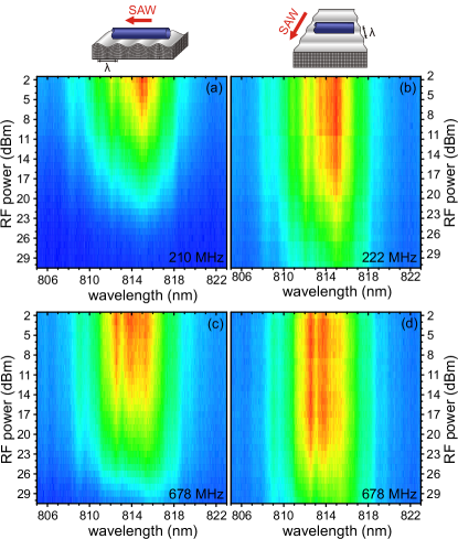
We investigated the SAW driven quenching of the NW emission in detail as a function of the SAW power, frequency and relative orientation of with respect to . The results of these experiments performed on NW1 are presented in 2. We plot the detected PL spectra normalized to the unperturbed emission in false color representation as a function of the applied RF power for low (high) frequency SAWs in the upper and lower upper panels, respectively. The relative orientation is and in the left and right panels as indicated by the schematics. In experiment we observe similar behavior of the NW emission for both SAW frequencies as we increase . For we observe a rapid and very pronounced quenching of the PL signal setting in at and for the low and high SAW frequencies. This dependence is in excellent agreement with a more efficient exciton dissociation within the Type-II band edge modulation with increasing SAW amplitude i.e. RF power. The reduced efficiency for the higher frequency is mainly attributed to a reduced coupling efficiency of the applied RF power to SAWs compared to the lower frequency. In strong contrast to planar, embedded nanostructures, we find that for both SAW frequencies the onset of the PL suppression is shifted significantly to and for compared to the parallel configuration. This experimentally observed, pronounced directionality of the emission suppression can be readily understood by taking into account the geometry of the inherently one-dimensional NWs. Clearly, the diameter of the NW is significantly smaller than the wavelength of the SAW whilst . Since defines the lengthscale on which carrier separation and exciton dissociation occur [c.f. 1 (a)], we expect the efficiency of this SAW-driven process to be significantly reduced (enhanced) for a SAW propagating perpendicular (parallel) to the which is nicely observed in our experimental data shown in 2. In addition we note that we do not resolve spectral shifts in our data, as observed e.g. for the narrow PL lines of QDs 14, *Metcalfe:10, 16 at large SAW amplitudes, due to the relatively broad emission peak of our NWs.
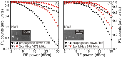
However, we have to exclude that the observed directionality does not arise from the anisotropic piezoelectric properties for SAW excitation in the down and left directions for the particular substrates used for our SAW device. As a first characterization we confirmed the comparable, efficient SAW generation both in the down and left directions by studying the diffraction efficiency of the SAW-induced amplitude grating 23. To fully confirm that the observed directionality arises from a more efficient exciton dissociation for compared to we performed identical experiments as presented for NW1 in 2 on NW2 which is rotated by 90o with respect to NW1. Thus, we expect the quenching of the emission of NW2 to be more efficient for a left propagating SAW compared to a down propagating SAW. In 3 we compare the integrated PL intensities detected from NW1 (a) and NW2 (b) as a function of . The presented experimental data clearly confirms that the emission of NW2 is more efficiently quenched by a SAW propagating to the left i.e. (left triangles) than by a SAW propagating down (down triangles) for both SAW frequencies studied. This directionality is completely reversed compared to NW1 proving that the observed anisotropy indeed arises only from the relative orientation of and .
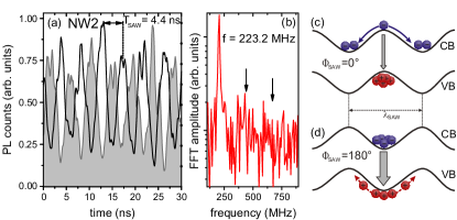
Up to now we neglected that this process itself is dynamic on a timescale defined by the period of the SAW . In order to resolve this fast dynamic modulation of the NW emission we perform TCSPC spectroscopy on the emission of NW2. In this experiment we measure the temporal correlation between the detected NW emission excited by a cw laser and the SAW. For low RF power applied at to IDT2 no modification of the total emission signal and, thus, no temporal correlations are observed. However, when we increase the RF power to , we find a clear modulation of the TCSPC signal as shown in the solid line in 4 (a). The period of the observed modualtion agrees well with the SAW period providing direct evidence for a dynamic acoustoelectric modulation of the NW emission on a nanosecond timescale. Moreover, only modulation with the fundamental period of the SAW and no contribution from higher harmonics (marked by arrows) are observed in the Fourier transform of the TCSPC signal [c.f. 4 (b)]. This modulation is characteristic for a diffusive exciton dissociation process in the SAW-induced band edge modulation schematically shown in 4 (c) and (d): At [4 (c)] holes are generated in an effective potential that is a stable maximum of the VB whilst electrons are located at a unstable maximum in the CB. This situation is reversed at at which electrons are generated at a stable minimum in the CB and holes at a unstable minimum in the VB [4 (d)]. Due to their higher mobility electrons diffuse rapidly from the point of generation for . This effect leads to a strong reduction of the electron density as indicated in 4 and consequently gives rise to the observed pronounced reduction of the PL emission. At electrons are captured at the stable minimum in the CB while at the same time hole diffusion is limited due to the higher effective mass and smaller mobility of this carrier species. Thus, the PL emission is only weakly suppressed at this local phase of the SAW corresponding to the maxima in the TCSPC signal. We note that similar observations have been reported for planar, fully embedded semiconductor heterostructures 13, 24 confirming our interpretation. This SAW-driven modulation requires that the PL decay time is significantly faster than 22. This condition would not be met in mixed crystal phase (zinc blende/wurtzite)NWs for which PL decay times can exceed several nanosconds21. To further support this model we performed a control experiment in which we shifted the phase of the SAW by with respect to the rising edge of the pulse used a the reference in the TCSPC experiment and plot the detected modulated signal in 4 (a). We find this histogram (gray shaded) offset by with respect to the original trace (line) corresponding to the externally set shift of the local SAW phase.
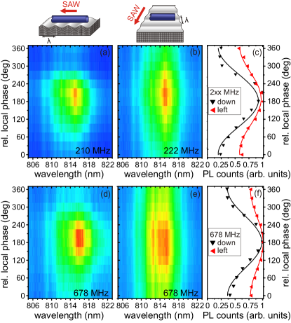
In the time-integrated experiments presented in Figures \plainreffig:1–\plainreffig:3 we averaged over all local phases of the SAW. By actively locking the to the RF signal used to excited the SAW, we are able to perform phase resolved spectroscopy 22 and resolve the dynamics of the emission modulation. In 5 we present normalized PL spectra as a function of plotted in false color representation. All spectra were recorded from NW1 and constant applied to the low frequency pair IDT1-IDT2 [c.f. 5 (a) and (b)] and the high frequency pair IDT3-IDT4 [c.f. 5 (d) and (e)], respectively. The relative orientation is and in the left and center panels as indicated by the schematics. For both frequencies we observe a clear and pronounced modulation of the emission intensity as we tune which directly reflects the local and dynamic modulation of the NW emission. As expected from the results obtained by phase-averaged spectroscopy, the contrast of the observed modulation is significantly reduced for [c.f. 5 (b) and (e)] compared to [c.f. 5 (a) and (d)]. We directly compare the amplitudes of these modulations by plotting the integrated PL intensity as a function of in 5 (c) and (f) for the low and high frequency SAWs. The observed directionality is again reflected in the reduced amplitudes of the oscillation for (left triangles) compared to (down triangles). Similar observations were also made for NW2 further confirming the directionality of the SAW-driven exciton dissociation in one-dimensional NWs.
| NW1, Phase-locking | 210 MHz/222 MHz | 678 MHz |
|---|---|---|
| NW2, TCSPC | 222 MHz | |
The experimentally measured modulations are well reproduced by least square fits of sine functions shown as lines in 5 (c) and (f) which we use to quantify the efficiencies of this process for the two configuration. As a figure of merit we define the relative dynamic suppression of the modulation
| (1) |
The obtained values of for and are summarized for all four IDTs in 1. From the ratio we can quantify the efficiencies of the dynamic PL modulation for a constant RF power to 3.6 and 2.6 for the low and high frequency SAWs, respectively. Remarkably, is almost identical for both frequencies which can be readily explained by the fast PL decay for uncapped, zinc blende phase GaAs NWs of governed by surface recombination25 which is almost two orders of magnitude faster than the period of the SAW. Due to this fast decay the SAW represents a quasi-static perturbation and the observed modulation reveals the dependency of the SAW-driven exciton dissociation as a function of the local phase of the SAW. Moreover, a comparison of the length scale on which electrons and holes are separated () and the diameter of the excitation laser focus (3 ) we would be expect a more pronounced reduction of when changing the SAW frequency by more than a factor of 3 from to 22. The weak but finite modulation and observed for SAWs excited by IDT2 and IDT4 could arise from the non-perfect alignment of the NW as seen in the SEM image in 1 (a). Furthermore we want to note that measured on NW1 for [c.f. 1] are in excellent agreement with extracted from the TCSPC data recorded from NW2 shown in 4 (a) at the same RF power.
In summary we have demonstrated fully dynamic and directional, SAW controlled modulation of the optical emission of single \ceGaAs NWs. The underlying separation of electrons and holes provides the foundation for elaborate schemes to transfer individual charges and spins in axial4, *Weert:09a, *Kouwen:10a and radial26, *Uccelli:10a nanostructures defined in this inherently scalable architecture. To achieve such deterministic charge conveyance losses due to surface recombination which is the dominant mechanism of unpassivated NWs, have to be overcome e.g. by using surface-passivated core-shell NW structures25. Moreover, a wide range of sophisticated architectures such as SAW-tunable crystal phase superlattices21, interdot couplings 28, *Stinaff:06, *Robledo:08 and advanced memory devices 31, *Heiss:09 or acoustically triggered generation of single photons 33, *Tribu:08a, 35, *Couto:09, *Voelk:10a and polarization entangled photon pairs 38 can be realized.
This work was financially supported by DFG via the cluster of excellence Nanosystems Initiative Munich (NIM) and SFB 631, by BMBF within the EPHQUAM consortium and by the European Union via SOLID, the Marie Curie FP7 Reintegration Grant (Christina Totte, project officer), and the TUM Institute of Advanced Study (IAS). G.K. would further like to thank A. Fontcuberta i Morral and E. Uccelli for helpful discussions.
Description of molecular beam epitaxy growth and parameters, SAW device fabrication, gating scheme for time- and SAW phase-resolved optical spectroscopy.
References
- Björk et al. 2004 Björk, M. T.; Thelander, C.; Hansen, A. E.; Jensen, L. E.; Larsson, M. W.; Wallenberg, L. R.; Samuelson, L. Nano Letters 2004, 4, 1621–1625
- Fasth et al. 2005 Fasth, C.; Fuhrer, A.; Björk, M. T.; Samuelson, L. Nano Letters 2005, 5, 1487–1490
- Pfund et al. 2007 Pfund, A.; Shorubalko, I.; Ensslin, K.; Leturcq, R. Physical Review Letters 2007, 99, 036801
- Björk et al. 2002 Björk, M. T.; Ohlsson, B. J.; Sass, T.; Persson, A. I.; Thelander, C.; Magnusson, M. H.; Deppert, K.; Wallenberg, L. R.; Samuelson, L. Applied Physics Letters 2002, 80, 1058–1060
- van Weert et al. 2009 van Weert, M. H. M.; Akopian, N.; Perinetti, U.; van Kouwen, M. P.; Algra, R. E.; Verheijen, M. A.; Bakkers, E. P. A. M.; Kouwenhoven, L. P.; Zwiller, V. Nano Letters 2009, 9, 1989–1993
- Kouwen et al. 2010 Kouwen, M. P. V.; Reimer, M. E.; Hidma, A. W.; van Weert, M. H. M.; Algra, R. E.; Bakkers, E. P. A. M.; Kouwenhoven, L. P.; Zwiller, V. Nano Letters 2010, 10, 1817–1822
- Gywat et al. 2009 Gywat, O.; Krenner, H. J.; Berezovsky, J. Spins in Optically Active Quantum Dots; Wiley-VCH, Berlin, 2009
- Hanson et al. 2007 Hanson, R.; Kouwenhoven, L. P.; Petta, J. R.; Tarucha, S.; Vandersypen, L. M. K. Reviews of Modern Physics 2007, 79, 1217
- Claudon et al. 2010 Claudon, J.; Bleuse, J.; Malik, N. S.; Bazin, M.; Jaffrennou, P.; Gregersen, N.; Sauvan, C.; Lalanne, P.; Gérard, J. Nature Photonics 2010, 4, 174–177
- Sogawa et al. 2001 Sogawa, T.; Santos, P. V.; Zhang, S. K.; Eshlaghi, S.; Wieck, A. D.; Ploog, K. H. Physical Review Letters 2001, 87, 276601
- Stotz et al. 2005 Stotz, J. A. H.; Hey, R.; Santos, P. V.; Ploog, K. H. Nature Materials 2005, 4, 585–588
- Rocke et al. 1997 Rocke, C.; Zimmermann, S.; Wixforth, A.; Kotthaus, J. P.; Böhm, G.; Weimann, G. Physical Review Letters 1997, 78, 4099 – 4102
- Alsina et al. 2002 Alsina, F.; Santos, P. V.; Schönherr, H.-P.; Seidel, W.; Ploog, K. H.; Nötzel, R. Physical Review B 2002, 66, 165330
- Gell et al. 2008 Gell, J. R.; Ward, M. B.; Young, R. J.; Stevenson, R. M.; Atkinson, P.; Anderson, D.; Jones, G. A. C.; Ritchie, D. A.; Shields, A. J. Applied Physics Letters 2008, 93, 081115
- Metcalfe et al. 2010 Metcalfe, M.; Carr, S. M.; Muller, A.; Solomon, G. S.; Lawall, J. Physical Review Letters 2010, 105, 037401
- Völk et al. 2010 Völk, S.; Schülein, F. J. R.; Knall, F.; Reuter, D.; Wieck, A. D.; Truong, T. A.; Kim, H.; Petroff, P. M.; Wixforth, A.; Krenner, H. J. Nano Letters 2010, 10, 3399 – 3407
- Ebbecke et al. 2008 Ebbecke, J.; Maisch, S.; Wixforth, A.; Calarco, R.; Meijers, R.; Marso, M.; Lüth, H. Nanotechnology 2008, 19, 275708
- Roddaro et al. 2010 Roddaro, S.; Strambini, E.; Romeo, L.; Piazza, V.; Nilsson, K.; Samuelson, L.; Beltram, F. Semiconductor Science and Technology 2010, 25, 024013
- Fontcuberta i Morral et al. 2008 Fontcuberta i Morral, A.; Colombo, C.; Abstreiter, G.; Arbiol, J.; Morante, J. R. Applied Physics Letters 2008, 92, 063112
- Koblmüller et al. 2010 Koblmüller, G.; Hertenberger, S.; Vizbaras, K.; Bichler, M.; Bao, F.; Zhang, J.-P.; Abstreiter, G. Nanotechnology 2010, 21, 365602
- Spirkoska et al. 2009 Spirkoska, D. et al. Physical Review B 2009, 80, 245325
- Völk et al. 2011 Völk, S.; Knall, F.; Schülein, F. J. R.; Truong, T. A.; Kim, H.; Petroff, P. M.; Wixforth, A.; Krenner, H. J. Applied Physics Letters 2011, 023109
- Ruppert et al. 2010 Ruppert, C.; Neumann, J.; Kinzel, J. B.; Krenner, H. J.; Wixforth, A.; Betz, M. Physical Review B 2010, 82, 081416(R)
- Alsina et al. 2003 Alsina, F.; Santos, P. V.; Schönherr, H.-P.; Nötzel, R.; Ploog, K. H. Physical Review B 2003, 67, 161305
- Demichel et al. 2010 Demichel, O.; Heiss, M.; Bleuse, J.; Mariette, H.; i Morral, A. F. Applied Physics Letters 2010, 97, 201907
- Fontcuberta i Morral et al. 2008 Fontcuberta i Morral, A.; Spirkoska, D.; Arbiol, J.; Heigoldt, M.; Morante, J. R.; Abstreiter, G. Small 2008, 7, 899–903
- Uccelli et al. 2010 Uccelli, E.; Arbiol, J.; Morante, J. R.; Fontcuberta i Morral, A. ACS Nano 2010, 4, 5985–5993
- Krenner et al. 2005 Krenner, H. J.; Sabathil, M.; Clark, E. C.; Kress, A.; Schuh, D.; Bichler, M.; Abstreiter, G.; Finley, J. J. Physical Review Letters 2005, 94, 057402
- Stinaff et al. 2006 Stinaff, E. A.; Scheibner, M.; Bracker, A. S.; Ponomarev, I. V.; Korenev, V. L.; Ware, M. E.; Doty, M. F.; Reinecke, T. L.; Gammon, D. Science 2006, 311, 636–639
- Robledo et al. 2008 Robledo, L.; Elzerman, J.; Jundt, G.; Atature, M.; Hogele, A.; Falt, S.; Imamoglu, A. Science 2008, 320, 772–775
- Krenner et al. 2008 Krenner, H. J.; Pryor, C. E.; He, J.; Petroff, P. M. Nano Letters 2008, 8, 1750 –1755
- Heiss et al. 2009 Heiss, D.; Jovanov, V.; Caesar, M.; Bichler, M.; Abstreiter, G.; Finley, J. J. Applied Physics Letters 2009, 94, 072108
- Borgström et al. 2005 Borgström, M. T.; Zwiller, V.; Müller, E.; Imamoglu, A. Nano Letters 2005, 5, 1439–1443
- Tribu et al. 2008 Tribu, A.; Sallen, G.; Aichele, T.; André, R.; Poizat, J.; Bougerol, C.; Tatarenko, S.; Kheng, K. Nano Letters 2008, 8, 4326–4329
- Wiele et al. 1998 Wiele, C.; Haake, F.; Rocke, C.; Wixforth, A. Physical Review A 1998, 58, R2680–R2683
- Couto et al. 2009 Couto, O. D. D.; Lazić, S.; Iikawa, F.; Stotz, J. A. H.; Jahn, U.; Hey, R.; Santos, P. V. Nature Photonics 2009, 3, 645–648
- Völk et al. 2010 Völk, S.; Schülein, F. J. R.; Knall, F.; Wixforth, A.; Krenner, H. J.; Laucht, A.; Finley, J. J.; Riikonen, J.; Mattila, M.; Sopanen, M.; Lipsanen, H.; He, J.; Truong, T. A.; Kim, H.; Petroff, P. M. Proc. SPIE 2010, 7610, 76100J
- Singh and Bester 2009 Singh, R.; Bester, G. Physical Review Letters 2009, 103, 063601–+