Unravelling the role of inelastic tunneling into pristine and defected graphene
Abstract
We present a first principles method for calculating the inelastic electron tunneling spectroscopy (IETS) on gated graphene. We reproduce experiments on pristine graphene and point out the importance of including several phonon modes to correctly estimate the local doping from IETS. We demonstrate how the IETS of typical imperfections in graphene can yield characteristic fingerprints revealing e.g. adsorbate species or local buckling. Our results show how care is needed when interpreting STM images of defects due to suppression of the elastic tunneling on graphene.
pacs:
72.10.Di,68.37.Ef,63.22.Rc,63.20.dkImperfections such as lattice defects, edges, and impurity/dopant atoms can degrade the superb transport properties of graphene,1; 2; 3; 4 or may, if controlled, lead to new functionality.5 Scanning Tunneling Microscopy/Spectroscopy (STM/STS) have been used extensively to obtain insights into the local electronic structure of graphene with atomic resolution.6; 7; 8; 9; 10 However, contrary to most STM/STS experiments where elastic tunneling plays the dominant role, for graphene the inelastic tunneling prevails. This was clearly demonstrated experimentally as a “giant” signal in the second derivative of the current w.r.t. voltage obtained in Inelastic Electron Tunneling Spectroscopy (IETS) performed on gated, pristine graphene with STM.6; 7; 8 The pronounced inelastic features are rooted in the electronic structure of graphene. The electrons have to enter the Dirac-points corresponding to a finite in-plane momentum leading to weak elastic tunneling. The IETS signal of pristine graphene has been reproduced qualitatively by Wehling et al. considering the change in the wavefunction decay when displacing the carbon atoms along a selected frozen zone-boundary out-of-plane phonon.11 In general, the important role of the inelastic process complicates the interpretation of STM results on graphene. Ideally STM images on graphene structures should be accompanied by local STS/IETS measurements, in order to distinguish between contributions from the inelastic and elastic channel. On the other hand, first principles calculations based on Density Functional Theory (DFT) often provide essential unbiased insights into STM/STS/IETS experiments to help the interpretation.
In this work we present a method for DFT calculations of the STS/IETS on gated
graphene. We demonstrate its predictive power by reproducing from first principles the
features of the experimental results for the giant inelastic conductance of gated
pristine graphene.6; 7; 8 We then provide results for IETS signals of defected graphene systems
determining the relative impact on the current of the various phonon modes. In particular
we identify inelastic fingerprints of selected defects, suggesting that IETS measurements
can be a powerful tool in the characterization of imperfect graphene. Our
analysis also illustrates how one should keep in mind the in-plane momentum conservation when
performing STM on graphene. In particular we demonstrate how defects can locally lift the suppression of elastic tunneling. The resulting increased local conductance may be misinterpreted as a high local density of states (LDOS).
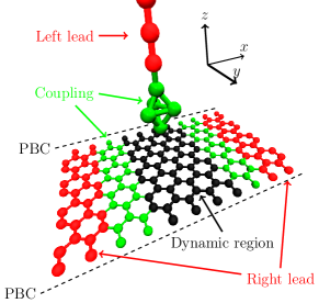
Method. The calculations are performed with DFT using the SIESTA/TranSIESTA 12; 13 code and the Inelastica package for inelastic transport.14 Our system shown in Fig. 1 is divided into device and “left”/“right” leads following the standard13; 14 transport setup. 111We use a split DZP basis set, a mesh cutoff of Ry, a Monkhorst-Pack -point mesh of 1x2x1 and the LDA xc-functional23 to calculate the electronic structure. Supercell dimension(-points) of /// is used for inelastic transport for the pristine/SW/edge/adsorbate configuration. We consider a suspended graphene sheet located Å below the tip of a gold STM probe model. The “left” semi-infinite lead is attached to the probe, while the “right” semi-infinite leads are attached at both sides of the graphene sheet. We consider a voltage bias between “left” and “right” leads. The electron-phonon coupling () is inherent to a coupling region (green black atoms in Fig. 1) of phonon modes (index ) calculated in a dynamical region (black atoms). Floating orbitals are included between the STM tip and the graphene sample, to give a better description of the exponential decay of tunneling conductance.16
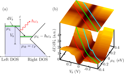
Following the Lowest Order Expansion (LOE),17 simplified and efficient expressions for the IETS signals can be derived under the assumption of weak electron-phonon coupling. The LOE expressions involve just the evaluation of the spectral density matrices for left/right moving states, , at the chemical potentials, , corresponding to the threshold voltage bias () for excitation of a given phonon (), . Thus the LOE expression does not per se reflect changes in the DOS above the phonon excitation threshold. However, in the context of STS on gated graphene, this is highly relevant since the behavior of the DOS leads to a distinct dip in the differential conductance at specific applied voltage, , 6 enabling a determination of the local chemical potential of graphene.
In order to encompass this important variation in the DOS above threshold we make the following observations (see also Fig. 2(a)). The expressions for the current which gives rise to inelastic signals have a form exemplified by the inelastic contribution to the current within LOE,
| (1) |
where is the time reversed left spectral function, and is the left/right occupation function. Here the coth-terms yield the IETS-signal, namely a sharp step in the differential conductance, , for at low temperature. Above threshold () the step behavior is unimportant and we are left with the bias-behavior of the integral. For finite bias both the filling of states () as well as the states in the device, that is, the spectral functions, change with . However, in this STM setup the device is strongly coupled to the right lead (graphene) and is very weakly coupled to the left lead (probe). Consequently the potential in the device is pinned to that of the right lead, which is the Fermi level of the gated graphene lead. The DOS of the gold STM probe varies slowly w.r.t. energy. Thus if we define with the right chemical potential fixed at , the only important voltage dependent term is the Fermi-function, inside the integral in Eq. (1) yielding an approximate -function in the differential conductance expression,
| (2) |
where
| (3) |
and is a universal function. 17 We are therefore again left with evaluating the spectral functions at only two energies, and . Equation 2 is equivalent to the usual LOE expression but valid above threshold due to the constant tip-DOS. The same argument can be applied to the other terms in LOE.
In practice we calculate the LOE differential conductance for a range of , see
Fig. 2(b), and can obtain the differential conductance by following the contour along
the direction (green line), and projecting it onto the , plane. Gating the graphene sheet corresponds to shifting the Fermi level by a
constant over all bias voltages, and can be obtained from Fig. 2(b) by a
translation of the contour along the chemical potential axis.
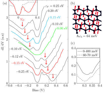
Results — pristine graphene. Calculated STS spectra on pristine graphene for a number of different Fermi levels are shown in
Fig. 3(a). The gap feature around of width V is reproduced in detail and the dip at , caused by inelastic tunneling into the charge neutrality point of graphene, appears outside the gap as seen in experiments.6; 7; 8 As the gate is applied, moves across the spectrum changing polarity while the position and
width of the gap feature is stable. The inset shows how significant the difference in results are when ignoring/including above threshold terms. It also shows how the usual LOE calculation works well
below threshold and captures the inelastic steps.
Most major steps in differential conductance come from acoustic out-of-plane phonons at energies just below meV.18 In particular the mode shown in Fig. 3(b) gives a large contribution.
However we find that acoustic out-of-plane graphene phonons with energies as
low as meV give considerable contributions as well. We also find important inelastic signals from optical graphene phonons at energies above meV. The additional features away from mV make up about half the signal, and have not been included in previous
studies.11 If we restrict our calculations to phonons in the – meV
range, we obtain a mV change in (), see Fig. 3(c), and changes in both the width and height of the inelastic gap. The change in is caused mostly by the experimentally observed8 inelastic signal near mV, coming from the optical in-plane modes, and occurs for mV.
In STS experiments is used to extract the energy position of the charge neutrality point from where meV is half the width of the gap feature which corresponds to the energy of an acoustic out-of-plane graphene phonon.6; 7
The change in could explain why all points with meV in the vs gate voltage plot of Ref.7 fall below the fitted line.
Local charge-carrier density () of graphene is also extracted from in STS experiments.7; 9; 10
Mistaking meV for meV results in a 32% error in .
To capture these experimental details one must include
several phonons, and account for their impact in an ab initio manner.
Encouraged by the agreement for pristine graphene we
next predict the inelastic signals from various defects to shed light on what information
can be obtained from STM-IETS.
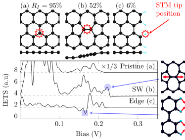
Results — Structurally defected graphene. In Fig. 4 we show the calculated IETS spectra from an on-top position in pristine
graphene (a), directly above a Stone-Wales defect (SW) (b), and above a passivated
armchair edge (c). The result shown for pristine graphene is the same at hollow sites and
bridge sites.
We find that the gap feature and low voltage IETS above a SW is very similar
to that of pristine graphene. The gap has also been observed experimentally for regions
with heptagon-pentagon defects.19
However, a characteristic signal can be seen at mV bias, above any of the pristine graphene phonon bands which can be traced to the high frequency stretch mode localized at the
twisted C-C bond shown in Fig. 4.
Ignoring the out-of-plane buckling introduced to the graphene sheet near a SW, and calculating the IETS for a flat SW system, leads to a mV blue-shift of the signal from the twisted C-C bond as previously proposed.20 We also see strong signals at low bias. These signals are caused by low-frequency sine-like out-of-plane modes. These modes couple strongly to the current because they break the mirror symmetry across the twisted C-C bond.
In the buckled system, this symmetry is inherently broken, leading to an increase in elastic tunneling.
Measuring strong low bias inelastic signals and a mV signal above a SW therefore indicates that it is in a metastable flat configuration, whereas increased elastic transmission and a mV signal is a sign of local buckling. Above a passivated armchair edge a dip in IETS is seen at mV caused by a collective transverse mode of the Hydrogen atoms shown in Fig. 4.
Changing the mass of the passivating agent to that of Fluor, we observe a corresponding change in the position of the inelastic signals. This indicates that IETS can be used to obtain knowledge of graphene edge passivation.
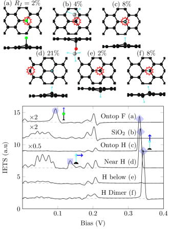
Results — Adsorbates on graphene. In Fig. 5 we show IETS spectra from a range of different covalently bonded
impurities (Fluor, Hydrogen) and a model of strong interaction to a SiO2 substrate. In Fig. 5(a) a
clear inelastic signal from the longitudinal mode of a Flour adsorbate is seen at mV. Above a Hydrogen adsorbate, we
see a strong inelastic peak at mV caused by the stretch mode of the C-H
bond (see Fig. 5(c)). This signal serves as a fingerprint for a Hydrogen impurity above the graphene sheet as opposed to below where the signal disappears as can be seen in Fig. 5(e). The corresponding STS spectra show a strong zero-energy peak21, this behavior is however expected for all covalently bonded impurities,22 above or below the sheet, and can therefore not be used as a fingerprint.
The STS spectra on the hydrogenated system with the probe above a Carbon atom
Å laterally away from the impurity in Fig. 5(d), shows additional signals.
The graphene out-of-plane phonon signals reappear and a signal is also seen at mV
caused by a transverse mode of the C-H bond.
Above a graphane-like hydrogen dimer Fig. 5(f) the signal caused by the C-H bond stretch mode is seen,
however here it is caused by two degenerate modes and blue-shifted by 11–16 mV indicating a lower energy configuration.
Common for all the imperfect systems is that the gap seen in pristine graphene is
quenched as indicated by the severe reduction of the inelastic conductance ratio () in Fig. 4 and 5. Out-of-plane corrugations in the graphene sheet can lift the suppression of
elastic tunneling if they are on the same length scale as the graphene lattice constant.11
Our results indicate that defects can also lift the suppression locally. This is because the selection rules causing the suppression
in pristine graphene is a result of the translational symmetry of the crystal lattice. When this symmetry
is broken the suppression is lifted and the elastic tunneling dominates. The expected
order of magnitude change in tunneling conductance should lead to bright spots in STM
topographies. In the case of granular CVD graphene protruding grain boundaries are often
attributed to localized electronic states.19 Our results here point out
that one may expect increased tunneling near disordered areas of graphene, even if no
localized electronic states are present and the area is completely flat.
As seen in Fig. 5(b)(e) this is also the case for strong interaction with a SiO2 substrate or adsorbates sitting below the graphene sheet, which should therefore be visible as protruding from the graphene sheet.
In summary, we have presented a first principles method and used it for calculations of IETS and STS spectra of pristine and defected graphene. We showed how measured STS spectra on pristine gated graphene can be reproduced in detail as a function of gating. The inclusion of several phonons had a strong impact on all aspects of the STS spectrum of pristine graphene. In particular we found that including optical in-plane phonons changed the value for certain gate voltages. This is of importance for studies where IETS is used to probe the local doping of graphene7; 9; 10 where it may lead to a significant overestimation of the local charge inhomogeneity. We predicted the IETS of typical imperfections in graphene, and demonstrated how these can yield characteristic fingerprints revealing e.g. adsorbate species or local buckling. Additional elastic contributions above defects should make them protrude in STM regardless of actual geometric or electronic structure and care is needed when interpreting STM images.
We gratefully acknowledge discussions with Thomas Frederiksen, Aran Garcia-Lekue and Rasmus Bjerregaard Christensen.
References
- Geim and Novoselov (2007) A. Geim and K. S. Novoselov, Nat. mat. 6(3), 183 (2007).
- Neto et al. (2009) A. H. C. Neto, F. Guinea, N. M. R. Peres, K. S. Novoselov, and A. K. Geim, Reviews of modern physics 81(1), 109 (2009).
- Novoselov et al. (2004) K. S. Novoselov, A. K. Geim, S. V. Morozov, D. Jiang, Y. Zhang, S. V. Dubonos, I. V. Grigorieva, and A. A. Firsov, Science 306, 666 (2004).
- Ferrari et al. (2006) A. C. Ferrari, J. C. Meyer, V. Scardaci, C. Casiraghi, M. Lazzeri, F. Mauri, S. Piscanec, D. Jiang, K. S. Novoselov, S. Roth, and A. K. Geim, Phys. Rev. Lett. 97, 187401 (2006).
- Pedersen et al. (2012) J. Pedersen, T. Gunst, T. Markussen, and T. Pedersen, Phys. Rev. B 86 (2012).
- Zhang et al. (2008) Y. Zhang, V. W. Brar, F. Wang, C. Girit, Y. Yayon, M. Panlasigui, A. Zettl, and M. Crommie, Nat. Phys. 4, 627 (2008).
- Decker et al. (2011) R. Decker, Y. Wang, V. W. Brar, W. Regan, H. Z. Tsai, Q. Wu, W. Gannett, A. Zettl, and M. F. Crommie, Nano Letters 11 (2011).
- Brar et al. (2010) V. W. Brar, S. Wickenburg, M. Panlasigui, C.-H. Park, T. O. Wehling, Y. Zhang, R. Decker, i. m. c. b. u. Girit, A. V. Balatsky, S. G. Louie, A. Zettl, and M. F. Crommie, Phys. Rev. Lett. 104, 036805 (2010).
- Cao et al. (2012) P. Cao, J. O. Varghese, K. Xu, and J. R. Heath, Nano Letters 12, 1459 (2012).
- Goncher et al. (2013) S. J. Goncher, L. Zhao, A. N. Pasupathy, and G. W. Flynn, Nano Letters 13, 1386 (2013).
- Wehling et al. (2008) T. O. Wehling, I. Grigorenko, A. I. Lichtenstein, and A. V. Balatsky, Phys. Rev. Lett. 101, 216803 (2008).
- Soler et al. (2002) J. M. Soler, E. Artacho, J. D. Gale, A. García, J. Junquera, P. Ordejón, and D. Sánchez-Portal, J. Phys.: Condens. Matter 14, 2745 (2002).
- Brandbyge et al. (2002) M. Brandbyge, J. L. Mozos, P. Ordejón, J. Taylor, and K. Stokbro, Phys. Rev. B 65, 165401 (2002).
- Frederiksen et al. (2007) T. Frederiksen, M. Paulsson, M. Brandbyge, and A. P. Jauho, Phys. Rev. B 75, 205413 (2007).
- Note (1) We use a split DZP basis set, a mesh cutoff of Ry, a Monkhorst-Pack -point mesh of 1x2x1 and the LDA xc-functional23 to calculate the electronic structure. Supercell dimension(-points) of /// is used for inelastic transport for the pristine/SW/edge/adsorbate configuration.
- Garcia-Lekue and Wang (2010) A. Garcia-Lekue and L. W. Wang, Phys. Rev. B 82, 035410 (2010).
- Lü et al. (2014) J. T. Lü, R. B. Christensen, G. Foti, T. Frederiksen, T. Gunst, and M. Brandbyge, Phys. Rev. B (2014).
- Mohr et al. (2007) M. Mohr, J. Maultzsch, E. Dobardzic, S. Reich, I. Milocevic, M. Damnjanovic, A. Bosak, M. Krisch, and C. Thomsen, Phys. Rev. B 76, 035439 (2007).
- Zhao et al. (2013) L. Zhao, M. Levendorf, S. Goncher, T. Schiros, L. Paova, A. Zabet-Khosousi, K. T. Rim, C. Gutierez, D. Nordlund, C. Jaye, M. Hybertsen, D. Reichman, G. W. Flynn, J. Park, and A. N. Pasupathy, Nano Letters 13, 4659 (2013).
- Ma et al. (2009) J. Ma, D. Alfe, A. Michaelides, and E. Wang, Phys. Rev. B 80, 033407 (2009).
- Scheffler et al. (2012) M. Scheffler, D. Haberer, L. Petaccia, M. Farjam, R. Schlegel, D. Baumann, T. Hänke, A. Gruneis, M. Knupfer, C. Hess, and B. Buchner, ACS Nano 6, 10590 (2012).
- Wehling et al. (2009) T. O. Wehling, M. I. Katsnelson, and A. I. Lichtenstein, Phys. Rev. B 80, 085428 (2009).
- Perdew and Zunger (1981) J. P. Perdew and A. Zunger, Phys. Rev. B 23, 5048 (1981).