Isolating electrons on superfluid helium
Abstract
Electrons floating on the surface of superfluid helium have been suggested as promising mobile spin quantum bits (qubits). Transferring electrons extremely efficiently in a narrow channel structure with underlying gates has been demonstrated, showing no transfer error while clocking pixels in a 3-phase charge coupled device (CCD). While on average, one electron per channel was clocked, it is desirable to reliably obtain a single electron per channel. We have designed an electron turnstile consisting of a narrow (0.8m) channel and narrow underlying gates (0.5m) operating across seventy-eight parallel channels. Initially, we find that more than one electron can be held above the small gates. Underlying gates in the turnstile region allow us to repeatedly split these electron packets. Results show a plateau in the electron signal as a function of the applied gate voltages, indicating quantization of the number of electrons per pixel, simultaneously across the seventy-eight parallel channels.
1 Introduction
Electrons are bound above the surface of liquid helium by their weak image potential as well as potentials from underlying electrostatic gates [12, 14, 4, 1]. These underlying gates control the position of electrons on helium and can move them across the sample into various regions [2, 10]. The electrons reside in vacuum, about 11nm above the surface, forming a very clean classical two dimensional electron system. Electron spins are expected to have little spin decoherence, due to the small spin-orbit interaction [6], allowing for the possibility of mobile spin qubits in a condensed matter system. To realize mobile spin qubits, control of individual electrons is necessary. With a single-electron transistor (SET) placed under the helium surface, individual electrons have been counted as they come in and out of a trap [8]. Electron transport of a single line of charge has been observed with a point constriction formed in a microchannel using a split gate [9]. We show that in addition to the confinement from a channel, narrow underlying gates perpendicular to the channel can be used to trap electrons over one electrostatic gate. The narrow channel and gates for isolating single electrons and wider channels with CCD’s are integrated, moving towards single electron control.
2 Device Structure
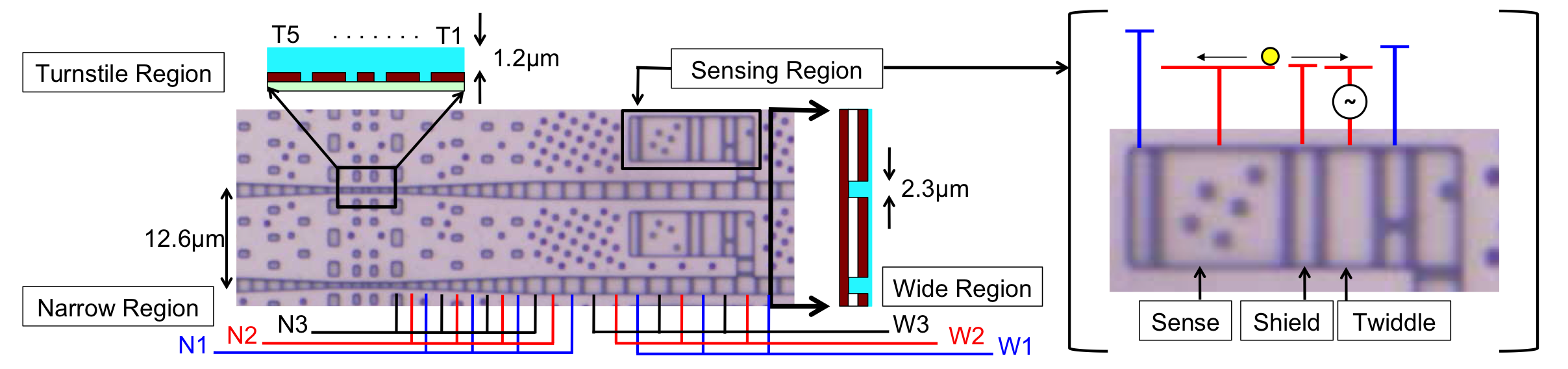
The complementary metal-oxide-silicon (CMOS) process is a standard foundry process that consists of multiple metal layers above a silicon substrate, with the metal layers separated by insulators. The helium channel device [7, 3, 10, 5, 9] with turnstiles was fabricated utilizing this technology. Seventy-eight parallel channels were designed using one of the metal layers as the top ground plane, with the metal layer below defining the gates that underlay all the channels as shown in Fig.1. The device consists of an electron collecting region to the right of the image in Fig.1, sensing region, wide CCD (WCCD) region, narrow CCD (NCCD) region, and a turnstile region. Electrons are collected over a wide underlying gate, termed plate, and clocked into 8.7m long pixels (note: three gates comprise a pixel, with a 2.9m gate period), both of which have 2.3m wide channels. The WCCD region is followed by a NCCD region with four three-phase pixels. The first NCCD has a 7.5m pixel length while it remains in a 2.3m wide channel. It then necks down to a 0.8m wide channel over three 6m period pixels. The NCCD section is followed by the turnstile region which contains five individual gates. The first two gates, designated T1 and T2, are 1m wide, with 0.4m spacing. The center gate, T3, is the narrowest gate (0.5m), with 0.4m spacing to the neighboring gates. The fourth and fifth gates, T4 and T5, have the same dimensions as the first two, which forms a symmetric turnstile region. Electrons are detected in the sensing region which branches out from the channel, creating a larger area for electrons to be detected through a capacitive coupling to a wide sense gate [2]. A small ac-voltage (Vac) is applied to the twiddle gate to push electrons on and off the sense, while a narrow gate between these two gates shields the direct capacitive coupling between them. The periodically induced voltage on the sense gate induced by the electrons at the frequency of Vac (111kHz) is buffered by a high electron mobility transistor (HEMT) and detected using a lock-in amplifier. The HEMT is mounted on the backside of the printed circuit board, on which the sample is wirebonded.
3 Electron Detection
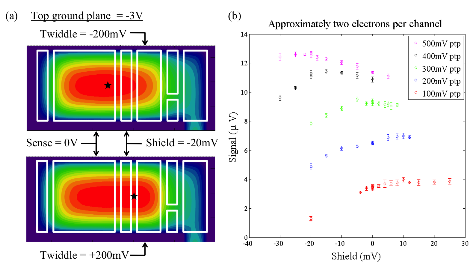
The large sense gate in the wider channels allows for improved electron detection due to a decreased coupling to the top ground plane. Figure 2 (a) shows the potential simulation of the sensing region when electrons are pushed on and off the sense gate. The star is placed at the potential energy minimum in each case. When electrons are pushed away from the twiddle gate the potential energy minimum is on the sense gate. When they are pulled towards the twiddle, the potential energy minimum is shifted away from the sense. The signal will increase as electrons are brought closer to the center of the sense and then pushed completely off the sense onto the twiddle. This is accomplished by applying a larger Vac on twiddle. Figure 2 (b) is a plot of measured electron signals from a range of applied voltages on the shield gate for different Vac on the twiddle gate. The signal increases as the amplitude of Vac increases, confirming that electrons are getting closer to the middle of the sense where the induced voltage will be maximized.
The potential energy minimum when electrons are pushed onto the sense gate could also be shifted by applying a small negative bias on the shield gate placed in between twiddle and sense. This also shifts the minimum away from the sense gate when electrons are pulled onto the twiddle gate. The experiments were performed with -20mV on the shield gate, and applying a 400mV twiddle Vac.
4 Experiment and Results
Electrons are photoemitted into the vacuum above the plate from a zinc film placed a few millimeters above the device [11]. Electrons collected on the plate are subsequently clocked into the sensing region using the WCCD gates. Starting with an arbitrary number of electrons per channel, these packets of electrons are brought into the NCCD gates. As the charge packet goes through the NCCD gates, the number of electrons that are allowed on each gate decreases as the channel narrows. Approximately 20 electrons per channel remain above turnstile gate, T1, when appropriate voltages are applied. These electrons are our initial charge packet. Other electrons that are not held on T1 are left behind above other gates, and these are clocked back into the plate. The initial packet of electrons are brought onto T2, T3, and T4 with +2V bias on those gates, while T1 and T5 are made repulsive at -3V, which is the same as the top ground plane bias. While voltage applied to T4 (VT4) is always held fixed at +2V, we chose a T2 voltage (VT2) to set a voltage difference, V = VT2 - VT4. For each measurement, V is chosen to make the potential well on the turnstile gates somewhat asymmetric. The voltage applied to T3 is gradually changed from +2V to -3V over 5 seconds, splitting the electron packet onto gates T2 and T4. The electrons above T2 are then clocked out from the turnstile, measured in the sensing region and brought into a gate in the wide channel for storage. The remaining electrons above T4 are again distributed onto gates T2, T3, and T4 by bringing the bias on T2 and T3 back to +2V with T1 and T5 at -3V. T2 is set to the same VT2, and the splitting sequence is repeated until no more electrons are found above T2 after splitting. Electrons above T4 are then brought back to the sensing region for measurement. These electrons are returned to those stored during the splitting and we perform the experiment again with the same group of electrons but a new V. Typical clock gate periods are 160 milliseconds. Given the rather low electron mobility at the operation temperature of 1.6K, hot electron effects are expected to be negligible at these time scales.
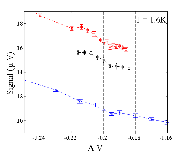
The signal, proportional to the number of electrons which were found above gate T4 at the end of the splitting process integrated across all seventy-eight channels, is shown in Fig.3 as a function of V. The asymmetry while splitting the electron packets with varying V determines the number of electrons left in T4. When there are many electrons in the turnstile approximately half of the electrons go onto T2 and the other half onto T4. After multiple “splits” there will be two electrons left, and the Coulomb repulsion assists the splitting of the electrons onto T2 and T4, as long as V is small (in magnitude) so the two electrons will prefer to split onto two gates, rather than both electrons residing above T4. This sets the lower bound of VT2 which would allow one electron on T4. When there is one electron in a channel, the electron will move onto T4 as long as V is large enough for the last electron to fall onto T4 instead of T2. This sets the upper bound of VT2, which would allow the final electron to go onto T4 after splitting. A plateau is seen in Fig.3 over multiple experiments between V = -0.20 and -0.18V. From finite element calculations, we find that applying 1V on either T2 or T4 changes the potential on the helium surface by 20meV and 1V on T3 changes the potential by 15meV. For most experiments, 4mV steps were taken on T2 gate, which corresponds to about 0.08mV (0.9K) on the surface. All the experiments are done at 1.6K, so the plateaus shown in Fig.3 are a few kT wide.
5 Conclusion
The existence of a plateau suggests a quantized electron signal, where the number of electrons per channel is fixed. Signal calibration using the measured capacitance (room temperature) and an estimate of the induced voltage on the sense gate with the parameters used in the experiments gives a signal of approximately 8.5V for one electron per channel when all seventy-eight channels are filled. The measured signal at the plateau region is between 10V to 16V. These values are larger than our estimate for a single electron per channel signal. If we take into account that not all the channels are filled with electrons, the measured signal approximately corresponds to two electrons per channel. The uniformity of electron occupation across the channels has been measured using a vertical channel as previously demonstrated [13]. We find that the number of channels filled with electrons varies from cooldown to cooldown with some empty channels at the top and bottom of the array. The smaller signal for the blue set of data points in Fig.3, as compared to the other two experiments probably arises from a larger number of empty channels in that experiment. From these considerations we conclude that the plateaus probably correspond to two electrons in a channel.
To investigate whether the plateaus in this region result from having one or two electrons per channel, detailed measurements at smaller V are necessary. Nonetheless, the plateaus seen in the measurements are a clear indication of the existence of a regime in which the number of electrons in a channel is always fixed, and that all the channels are operating simultaneously to quantize the charge with one set of gate voltages.
Acknowledgments
We would like to thank J. Donnal for the electronics to apply clock voltages to the CCD. Work at Princeton was supported by the NSF under Grant No. DMR-1005476.
References
- [1] Eva Y. Andrei, editor. Two-dimensional electron systems on helium and other cryogenic substrates. Kluwer Academic Publishers, 1997.
- [2] F. R. Bradbury, Maika Takita, T. M. Gurrieri, K. J. Wilkel, Kevin Eng, M. S. Carroll, and S. A. Lyon. Efficient clocked electron transfer on superfluid helium. Phys. Rev. Lett., 107:266803, 2011.
- [3] P Glasson, S.Erfurt Andresen, G Ensell, V Dotsenko, W Bailey, P Fozooni, A Kristensen, and M.J Lea. Microelectronics on liquid helium. Physica B: Condensed Matter, 284-288:1916–1917, 2000.
- [4] C. C. Grimes. Electrons in surface states on liquid helium. Surface Science, 73:379–395, 1978.
- [5] Hiroki Ikegami, Hikota Akimoto, and Kimitoshi Kono. Nonlinear transport of the wigner solid on superfluid he4 in a channel geometry. Phys. Rev. Lett., 102:046807, Jan 2009.
- [6] S. A. Lyon. Spin-based quantum computing using electrons on liquid helium. Phys. Rev. A, 74:052338, 2006.
- [7] D Marty. Stability of two-dimensional electrons on a fractionated helium surface. Journal of Physics C: Solid State Physics, 19:6097, 1986.
- [8] G. Papageorgiou, P. Glasson, K. Harrabi, V. Antonov, E. Collin, P. Fozooni, P. G. Frayne, M. J. Lea, D. G. Rees, and Y. Mukharsky. Counting individual trapped electrons on liquid helium. Applied Physics Letters, 86:153106, 2005.
- [9] D. G. Rees, I. Kuroda, C. A. Marrache-Kikuchi, M. Höfer, P. Leiderer, and K. Kono. Point-Contact Transport Properties of Strongly Correlated Electrons on Liquid Helium. Phys. Rev. Lett., 106:026803, 2011.
- [10] G. Sabouret, F. R. Bradbury, S. Shankar, J. A. Bert, and S. A. Lyon. Signal and charge transfer efficiency of few electrons clocked on microscopic superfluid helium channels. Applied Physics Letters, 92:082104, 2008.
- [11] S. Shankar, G. Sabouret, and S. A. Lyon. A low power photoemission source for electrons on liquid helium. Journal of Low Temperature Physics, 161:410–416, 2010.
- [12] W. T. Sommer. Liquid helium as a barrier to electrons. Phys. Rev. Lett., 12:271, 1964.
- [13] Maika Takita, F. R. Bradbury, T. M. Gurrieri, K. J. Wilkel, Kevin Eng, M. S. Carroll, and S. A. Lyon. Spatial distribution of electrons on a superfluid helium charge coupled device. Journal of Physics: Conference Series, 400:042059, 2012.
- [14] R. Williams and R. S. Crandall. Surface-state lifetimes and current flow in liquid helium. Phys. Rev. A, 4:2024, Nov 1971.