Finger-gate manipulated quantum transport in Dirac materials
Abstract
We investigate the quantum transport properties of multichannel nanoribbons made of materials described by the Dirac equation, under an in-plane magnetic field. In the low energy regime, positive and negative finger-gate potentials allow the electrons to make intra-subband transitions via hole-like or electron-like quasibound states (QBS), respectively, resulting in dips in the conductance. In the high energy regime, double dip structures in the conductance are found, attributed to spin-flip or spin-nonflip inter-subband transitions through the QBSs. Inverting the finger-gate polarity offers the possibility to manipulate the spin polarized electronic transport to achieve a controlled spin-switch.
1 Introduction
Dirac materials described by the Dirac equation for relativistic particles is a quickly developing field in low-dimensional mesoscopic systems that provides a wide field for both fundamental theoretical research and applications. One of the most well known examples is graphene where the electrons at the Fermi energy behave as relativistic massless particles [1, 2]. Graphene is a promising material for integration in nanoscale devices due to its high carrier mobility, and therefore has been considered for implementation in semimetals [1], nanoelectronics[3], coherent devices [4], and field-effect transistors [5]. However, its application on nanoelectronics is limited due to the lack of band gap at the Fermi energy. A well-established method to overcome this problem is by patterning graphene sheets into long stripes known as nanoribbons with varying widths using planar technologies of electron beam lithography and etching [6, 7, 8, 9, 10]. For example armchair graphene nanoribbons possess a gapped energy subband structure tunable by controlling the nanoribbon width [11, 12]. For some other celebrated examples, a considerable gap can be created by embending graphene on boron nitride (BN) substrates[13, 14, 15], or by impurity doping[16].
In recent years, there has been an extensive searching for alternative monolayer systems similar to graphene that would be more appropriate for nanoelectronics. One of the most recent examples is transition metal dichalcogenides (TMD) monolayers[17, 18, 19, 20, 21, 22, 23, 24, 25], two-dimensional monolayers with honeycomb lattice structures similar to graphene but with gapped subband stuctures of multi-valleys located at the K and K′ of the Brillouin zone. In contrast to graphene, a TMD monolayer can be described effectively by the massive Dirac equation instead of the massless one. Typically the energy band gap of TMD monolayers can be relatively large, for instance, 1.35 eV for W or 1.83 eV for Mo. Additionally, they offer certain advantages over conventional semiconductors, such as large spin-orbit (SO) coupling, which makes them promising candidates for spintronics applications.
Spintronics of conduction electrons is an emerging field due to its applications from logic to storage devices with high speed and very low power dissipation [26, 27, 28]. Manipulating the spin information offers the possibility to scale down spintronic devices to the nanoscale and is favorable for applications in quantum computing [29, 30, 31]. Various SO effects provide a promising way to spin manipulation in two-dimensional (2D) electron gases[32, 33]. Particularly, the Rashba SO interaction is of importance in spintronic devices, such as spin field-effect transistors [34, 35, 36].
In the current work, we propose a way of manipulating the quantum transport properties of spin-polarized electrons in nanoribbons made of massive Dirac materials, by using experimentally achievable finger-gate potential structures [37]. It is well known that a single impurity in open 2D quantum systems at the presence of magnetic field, may yield quasibound states (QBSs) below the subband bottoms of the energy spectrum, which can lead to strong backscattering of the conduction electrons, resembling evanescent scattering effects [38, 39, 40]. We shall demonstrate the role of the QBSs in Dirac nanoribbons under an in-plane magnetic field. We show that the QBSs lead to dips in the conductance, suppressing the spin-polarized electronic current of the nanoribbons, similarly to localized evanescent modes. The position of the dips can be controlled by the polarity (sign) of the finger-gate potential, offering the possibility for the realization of a spin-switch. The effects of the QBSs can be detected in the low energy regime via scattering processes involving one subband which we identify as intra-subband scattering and in the high energy regime, via scattering processes involving different subbands which we identify as inter-subband scattering. These processes can involve either flipping of the electron spin (spin-flip), or not (spin-nonflip), allowing additional control over the spin polarized electronic transport via partial finger-gate structures.
2 Model
In this section, we introduce a general tight-binding model to calculate the transport properties in nanoribbons made of Dirac materials influenced by an external in-plane magnetic field. The general equation that defines Dirac materials is the massive Dirac equation[41, 42, 43, 44, 45, 46]
| (1) |
where is the Fermi velocity of electrons depending on the material under investigation, and are the Pauli matrices. Symbol denotes the non-equivalent valleys that are present in graphene at the corners of its hexagonal Brillouin zone, and other Dirac materials like TMD monolayers. Eq. (1) describes relativistic particles with mass , where the speed of light is replaced by . Different values of classify different materials for example eV and m/s correspond to graphene while finite could correspond to TMD monolayers and graphene on BN substrates[15, 41, 43, 44].
A simple way to generate both Rashba and Zeeman effects is via applying a rotating in-plane magnetic field with tunable strength and rotation period that can be achieved experimentally by nanomagnets placed at the nanoribbon edges [41]. The resulting Rashba term is
| (2) |
where is the Pauli matrix while the Rashba interaction strength is given by . Alternatively this Rashba effect can be introcuced in the system by considering an electric field along . The rotating in-plane magnetic field induces also a Zeeman term
| (3) |
where the Zeeman interaction strength is given by . Notice that the spin quantization axis determined by the Rashba term () is perpendicular to the one determined by the Zeeman term (). This feature is important for the formation of QBSs at the edges of the subbands and can be achieved by different configurations of external magnetic and electric fields [37].
In order to perform our numerical calculations, we transform Eq. (1) to an effective Hamiltonian in the tight-binding formulation, consisting of a honeycomb lattice with an onsite staggered potential described by
| (4) |
where () is the creation (annihilation) operator for spin at site while is a uniform nearest neighbor hopping between all the lattice sites. The onsite potential is and on and sublattice sites respectively with corresponding to graphene. The staggered potential breaks the inversion symmetry resulting in a gap at the Fermi energy for the graphene nanoribbons that were originally metallic. At low energies the effective tight-binding Hamiltonian Eq. (4) is equivalent to Eq. (1) with where is the lattice constant. In this sense Eq. (4) can be thought as a numerical version of the massive Dirac equation. For numerical stability we fix eV and eV for the numerical calculations we present in the manuscript which results in a gap that is comparable to the gaps observed in TMD monolayers. However our findings concern any value of which could characterize a wide range of Dirac materials. We provide the general conditions to investige the QBS effects in various Dirac materials.
In order to constract a coordinate independent form of Eq. (2) in the tight-binding formulation we modify the full Rashba interaction term originated from an external electric field along [41, 47],
| (5) |
where is the spin vector with being the Pauli matrices, while the unit vector points along the bond connecting nearest neighbor sites i and j and points along . By considering only the part of Eq. (5) that contains and replacing it with [41] we can simulate as follows
| (6) |
We fix the Rashba interaction strength to meV which corresponds to nm for all the calculations presented in the manuscript.
The Zeeman term Eq. (3) is introduced in the tight-binding model via
| (7) |
where we fix also 0.05 meV, corresponding to T. The total effective tight-binding Hamiltonian of the system under investigation is
| (8) |
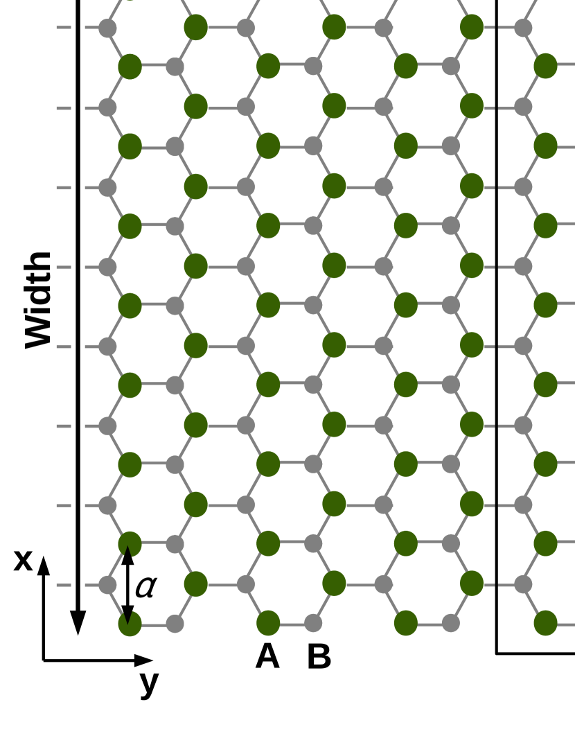
We consider hard-wall boundary conditions along forming nanoribbons with armchair edges in order to avoid edge effects. We fix the nanoribbon width to 8 corresponding to eight hexagons along perpendicular to the transport direction (figure 1).
The energy dependence of the conductance , in units of conductance quantum , is calculated via a recursive Green’s function method within the framework of Landauer-Büttiker formalism [48, 49]. To analyze the evanescent effects associated with the quasibound-state feature, we utilize a finger-gate potential as a scatterer, simulated by a uniform onsite potential on every site inside one unit cell of the armchair Dirac nanoribbon in the effective tight-binding model, as shown in figure 1. We also consider partial finger-gates by placing only on a few sites inside the unit cell. The corresponding partial density of states (PDOS) can be expressed in terms of the Green function element on site inside the scatterer with being the incident energy, being the scatterer Hamiltonian, and being the self energy of the left(right) lead, as
| (9) |
This quantity is useful for illustrating the QBS feature when the site is considered as a substitutional scatterer.
3 Subband Structure
In this section, we shall analyze the spectrum of the Dirac nanoribbon. Moreover, we shall show analytical expressions to describe the lowest conduction subbands in the presence of the Rashba spin-orbit interaction and the Zeeman effect due to the presence of the in-plane magnetic field.
In the absence of magnetic field, when only Eq. (1) is considered, the lowest conduction subbands, which we characterize by , follow a parabolic form for small corresponding to the massive Dirac fermions
| (10) |
where is the minimum energy of each subband.
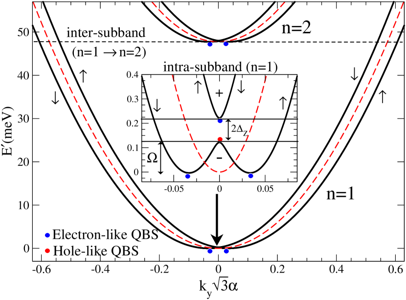
The numerical subband structure can be seen in figure 2, where we plot the shifted incident energy
| (11) |
as a function of rescaled longitudinal wave number . We use the energy for all the numerical calculations in the manuscript.
The red dashed curves in the main figure are the two lowest conduction subbands of denoted by and , with minimum energies meV, meV in Eq. (10). In the absense of magnetic field every subband is doubly degenerate in spin (Kramers degeneracy), corresponding to right and left propagating modes.
The inclusion of the Rashba term Eq. (2), described in tight-binding terms by Eq. (6), causes a spin-splitting along the transport direction creating two different branches for every subband represented by the black curves in figure 2. The branches are characterized by opposite spin polarizations, denoted by and in figure 2. However the Kramers degeneracy of the spin is preserved in this case. The Rashba spin-splitting mechanism is equivalent to a spin dependent shift of the wave vector resulting from the fact that the spin is a good quantum number for the Hamiltonian Eq. (1)[41].
The Kramers degeneracy of the spin is lifted by the Zeeman term Eq. (3), since the corresponding spin quantization axis () is perpendicular to the one determined by the Rashba term Eq. (2) (). Consequently a SO gap =0.1 meV opens at between the opposite spin branches originally created by the Rashba interaction. The SO gap can be seen in the inset of figure 2. Inside the gap there is one right and one left propagating mode characterized by opposite spin polarizations meaning that electrons traveling in opposite directions have opposite spins, creating a helical regime. This feature is important in quantum transport measurements since it leads to spin polarized current. The actual spin orientation along the branches for a given depends on the energy difference between the opposite spin branches, however the electrons are almost fully spin polarized along the direction (parallel or antiparallel) as long as the incident energy of the electrons coming from the leads is tuned higher than the middle of the SO gap [41].
The subband structure in the inset of figure 2 resembles the energy dispersion of an electron in a homogeneous 2D quantum wire at the presence of an in-plane magnetic field [37]. By plugging the Rashba-shifted wave vector , and the Zeeman effect (gap) in Eq. (10) we obtain an analytical formula that describes the branches of the subband , given by
| (12) |
where with the factor obtained by fitting the numerical subband structure in figure 2. This fitting factor is related to the honeycomb lattice morphology. The symbol indicates the two different branches with opposite spin polarizations. The energy is the corresponding modified ground state electronic energy in the quantum wire model
| (13) |
The corresponding effective Rashba interaction strength is while the Zeeman strength remains the same . The corresponding kinetic energy of the electron would be . The simple quantum wire model with in-plane magnetic field, with the effective parameters mentioned above could effectively describe the electron behavior in Dirac nanoribbons at the presence of a rotating in-plane magnetic field.
Based on Eq. (12), we define the spin-resolved branches of the subbands as , so that and ( and ) represent, the lower and upper branches of the first (second) subband =1 (=2).
The red and blue dots in figure 2 at the edges of the subband branches, correspond, to the hole-like QBS (HQBS) and electron-like QBS (EQBS), respectively, formed under the influence of the magnetic field. Under certain conditions the QBSs are known to induce backscattering in mesoscopic conductors, similarly to localized evanescent modes [38, 39, 40]. A finger-gate potential provides a convenient way to investigate the QBS effects in Dirac materials. The two EQBSs (blue dots) at the minima of the branch in the inset of figure 2 are located slightly lower than meV, due the Zeeman interaction. The HQBS (red dot) at the maxima of is located at energy meV. In analogy an EQBS is located at the minima of the upper branch at meV. The Zeeman gap is .
From the subband structure in figure 2, two types of scattering processes associated with the QBSs can be distinguished. One is intra-subband occurring between different branches belonging to same subband for example from branch to either the maximum of the same branch or to the bottom of , as shown by solid lines in the inset of figure 2. Additionally, inter-subband scattering can occur at higher energy between branches belonging to different subbands, denoted by a dashed line from =1 to =2 in figure 2. These transitions correspond to the scattering from either or , to the subband bottoms of . When a scattering process involves transitions between branches characterized by opposite then it corresponds to spin-flip backscattering through the QBS. For instance the intra-subband scattering process, to is spin-flip, while the inter-subband process to in spin-nonflip. We expect spin-flip scattering processes to occur at higher energies than the spin-nonflip ones, offering additional possibilities to control the the quantum transport properties of the spin-polarized electrons through finger-gate structures.
The width of the low energy regime of the branch () denoted by in the inset of figure 2 plays an important role. Considering only the Rashba interaction, it is proportional to the second term of Eq. (13) namely
| (14) |
obtained by putting and in Eq. (12). Increasing results in a quadratic increase of . On the other hand, increasing results in less steep slope of the subbands which reduces the effect of the Rashba spin splitting along , effectively decreasing . This behavior is retained for finite which simply opens a SO gap between the opposite spin branches created by the Rashba interaction. The interplay between and and it’s effect on is important for identifying the QBS scattering mechanism as we shall demonstrate below.
4 Intra-subband Scattering
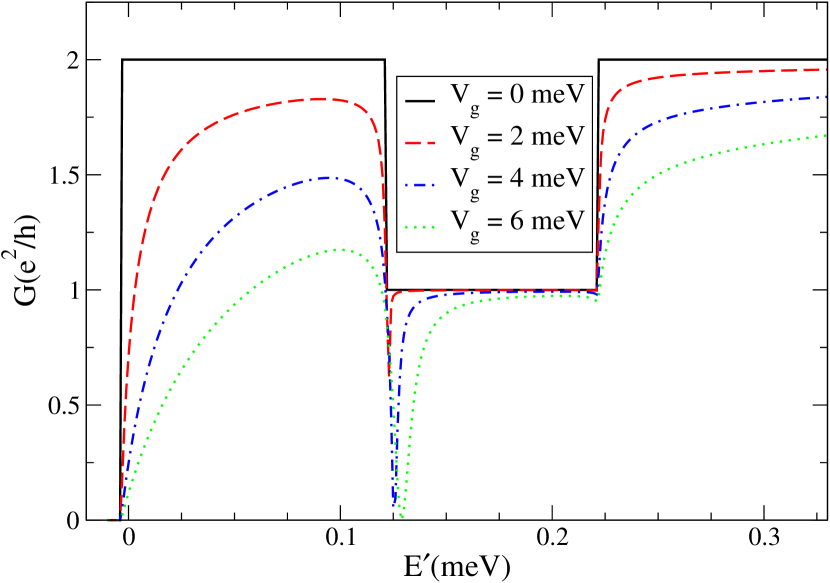
In this section, we demonstrate the intra-subband scattering effects within the Zeeman induced SO gap, shown in the inset of figure 2. The conductance versus the shifted energy for the subband =1 can be seen in figure 3 and figure 4 for positive and negative finger-gate potential strengths. Also, the case of ballistic transport without the finger-gate potential (Vg=0 meV) is also shown agreeing with the band structure in the inset of figure 2 leading to maximum conductance =1 inside the Zeeman gap and to =2 outside. For the case of positive potential in figure 3, the effect of the corresponding HQBS at the low end of the SO gap near ,can be clearly seen as a sharp dip suppressing the conductance. The dip widens as the potential strength increases while its position varies slightly also. For large potential strengths e.g for meV the conductance is completely suppressed (). Inverting the finger-gate potential, which corresponds to negative in figure 4 a similar dip is created at the high end of the SO gap near where an EQBS lies. Positive (negative) finger-gate potential leads to evanescent scattering via HQBS(EQBS) located near () in the inset of figure 2, suppressing the conductance near the edges of the Zeeman induced SO gap. We notice that the intra-subband scattering involves both spin-flip and spin-nonflip scattering processes. The dip induced by the negative finger-gate potential is a spin-flip process since it is caused by a transition between opposite spin branches, from to . On the other hand the dip induced by the positive finger-gate potential is a spin-nonflip process since it involves only the lower branch . The energy for the spin-flip process is higher that the spin-nonflip one.
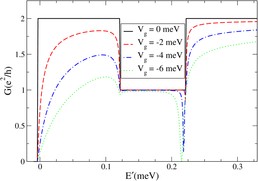
The intra-subband mechanism can be used as a spin-switch. By fixing the Fermi energy near either or at the edges of the SO gap, and inverting the polarity of the finger-gate potential it is possible to switch on and off the spin polarized electronic current. This mechanism would be more appropriate for energies near where the electrons have accumulated full spin polarization along the axis[41].
The intra-subband mechanism is not affected by the width of the ribbon since the parabolic form (Eq. (10)) of the =1 subband and the spin splitting caused by the Rashba and Zeeman terms described analytically by Eq. (12) are maintained for any ribbon width. Moreover the intra-subband scattering can be detected also for a few subsequent subbands like the =2 in figure 2. We have derived results similar to the ones shown in figure 3 and figure 4 for the two branches of the =2 subband, which can be seen in figure 5. Also, enlarging the range of the finger-gate will introduce multiple scattering effects, and hence reduce slightly the conductance, but the essential transport properties will not change.
The evanescent effects induced by the QBSs can be observed for different values of the staggered potential which corresponds to different Dirac materials. For instance, in the meV limit, which corresponds to armchair graphene nanoribbons the QBS effects can be detected for the semiconducting ribbons with gap, whose low energy subband structure resembles the inset of figure 2 [50]. For finite , the extent of the dips and the level of suppression of the conductance depends on fine-tuning the gate-potential strength along with the rotation period of the magnetic field which determines the Rashba strength . The width of the low energy regime of the branch (see Eq. (14)), shown in the inset of figure figure 2, plays an important role. We have found that in order to distinguish the QBS dips clearly should be much larger that , which can be roughly expressed as
| (15) |
in terms of and V. In principle, for any Dirac material, a fine-tuning of the magnetic field parameters and according to Eq. (15) should achieve the desirable conductance suppression which is required for better control of the spin-switch. Another necessary condition is that the Zeeman gap () determined by the magnetic field strength should be sufficiently large so that the EQBS and HQBS are clearly separated. In general, since Eq. (15) is inversely proportional to V, Dirac materials with large gaps like TMD monolayers require smaller than materials with smaller gaps, like graphene on BN substrates.
5 Inter-subband scattering
An additional scattering mechanism is possible between branches corresponding to different subbands , denoted by a dashed line between =1 and =2 in the subband structure shown in figure 2. Two scattering processes are possible, from either or , to the subband bottoms of . These processes create additional possibilities to control the electronic transport via partial finger-gate structures.
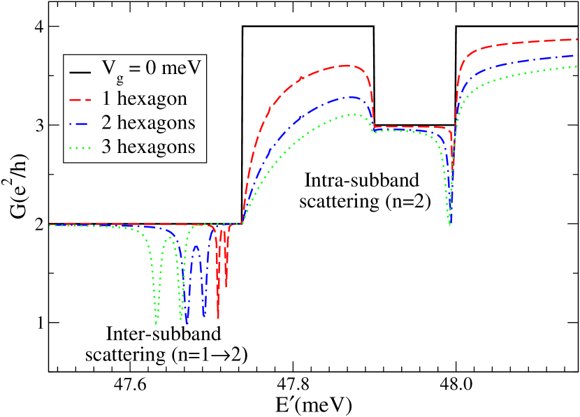
Since the inter-subband effects manifest due to electron-like QBS(EQBS) we need to use negative finger-gate potential in order to detect them. Additionally in order to enhance the inter-subband mechanism, one needs to break the symmetry of the ribbon along the direction, perpendicular to the transport[49]. To this end, we utilize a partial finger-gate potential constructed by choosing only a part of the complete finger gate consisting of one, two, or three hexagons, to place the onsite potential . The corresponding partial finger-gate widths would be 1, 2, or 3, respectively. The conductance as a function of the shifted energy is shown in figure 5 for different partial finger-gate potential areas for constant gate-potential strength meV. The effect of the intra-subband scattering is retained for the branches leading to a sharp dip at the high end of the SO-Zeeman gap as in the case of the scattering occurring between the branches of the subband .
In figure 5, the effects of the inter-subband scattering can be seen as a pair of sharp dips before the conductance jumps from G=2 to G=4 at due to the two additional channels opening from the two branches and . The two dips in each pair are caused by different types of scattering, namely the spin-flip and spin-nonflip scattering mechanisms. The dip occuring at higher energy comes from the spin-flip transition between the branch and the two EQBS lying at the bottoms of the branch (blue dots) in figure 2. On the other hand, the dip with the lower energy in each pair comes from the spin-nonflip transition between the branches and . The energy separation between the dip pair is getting larger by increasing the area of the partial finger-gate potential.
We notice that when the finger-gate occupies two and three hexagons, the conductance at each dip is suppressed approximately at leaving practically only one open channel for the conduction of electrons coming either from the or the branch that are characterized by opposite spin polarizations. This fact implies that the remaining current at each dip is spin polarized, with opposite spin polarization between the dips of each pair. The inter-subband induced dips cannot be detected with positive finger-gate potential.
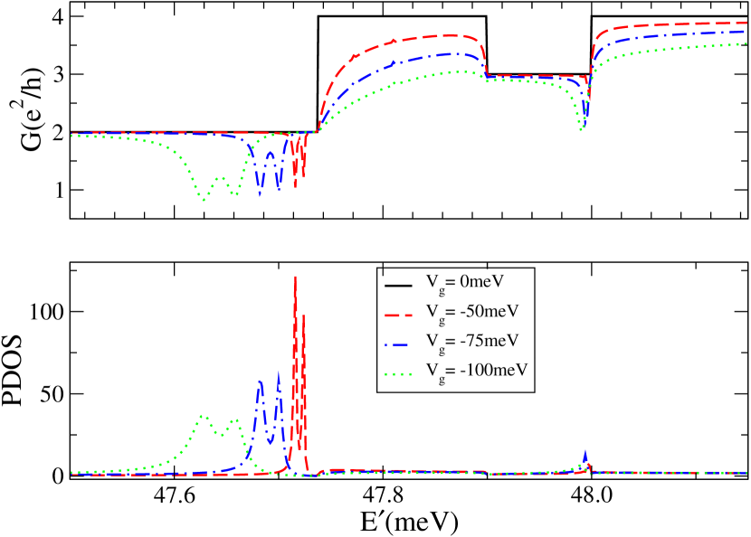
Due to these features the inter-subband scattering could be utilized to create and control spin polarized electronic transport. For instance, by inverting the polarity of finger-gate from positive to negative for a constant energy at the position where the dips occur, creates spin polarized transport with for sufficiently large finger-gate potential widths. In addition, by varying the Fermi energy of the Dirac nanoribbon between the dips in each pair the spin polarization of the remaining current is inverted. An alternative method to generate similar effects is to consider one single impurity at one-site at the edge of the nanoribbon. The result can be seen in figure 6 for various potential strengths. The PDOS shown in the bottom becomes maximum at the position of the conductance dips, indicating the quasi-localized QBSs. Using larger potential is roughly equivalent to using larger area of the partial finger-gate, both resulting in stronger backscattering. We note that the inter-subband mechanism is valid for any nanoribbon width since it involves transitions between different subbands which become more dense for wider nanoribbons. The level of control of the spin polarized transport for different corresponding to different Dirac materials depends on the fine-tuning of the magnetic field in conjunction with the finger-gate potential strength.
6 Concluding Remarks
We have proposed an experimentally achievable finger-gate manipulation of the spin-polarized electronic transport in nanoribbons made of Dirac materials under an in-plane magnetic field. A numerical tight-binding model has been utilized to calculate the subband structures and spin-resolved electronic transport involving intra-subband and inter-subband transitions.
The QBSs at the edges of the subband branches due to the Rashba and Zeeman effects result in conductance dips at the ends of the induced SO gap, via intra-subband transitions. The dip positions alternate between the low and the high end of the SO gap depending on the polarity of the finger-gate, allowing the realization of a spin-switch that can control the spin-polarized electronic transport. Additionally, inter-subband transitions are possible between different subbands. These transitions can be either spin-flip or spin-nonflip, creating pairs of dips in the conductance, since the energy required by each type of process is different. For any Dirac material, a combined fine-tuning of the magnetic field in conjuction with the finger-gate potential strength could provide the desirable optimal level of control for the spin-switch.
To summarize we have demonstrated the control of transmission spectra through Dirac nanoribbons using a tunable finger-gate setup to dramatically influence the quantum transport. Conductance drops can be created around the upper or lower bound of the Zeeman induced SO gap depending on the polarity of the finger-gate potential. This feature opens up a possibility for building quantum switch devices based on Dirac materials. We provide also additional ways to control the transmission spectra in the high energy regime via partial finger-gate structures.
7 Acknowledgements
We are grateful to Victor A. Gopar for valuable discussions. This work was supported by Ministry of Science and Technology, Taiwan through No. MOST 103-2112-M-239-001-MY3, and National Science Council through No. NSC 102-2112-M-009-009-MY2.
References
References
- [1] K. S. Novoselov, A. K. Geim, S. V. Morozov, D. Jiang, Y. Zhang, S. V. Dubonos, I. V. Grigorieva, A. A. Firsov, Sience 306, 666, (2004).
- [2] A. Castro Neto, F. Guinea, N. Peres, K. Novoselov, and A. Geim, Rev. Mod. Phys. 81, 109 (2009).
- [3] C. Berger, Z. Song, T. Li, X. Li, A. Y. Ogbazghi, R. Feng, Z. Dai, A. N. Marchenkov, E. H. Conrad, P. N. First, and W. A. de Heer, J. Phys. Chem. 108, 19912 (2004).
- [4] C. Berger, Z. Song, X. Li, X. Wu, N. Brown, C. Naud, D. Mayou, T. Li, J. Hass, A. N. Marchenkov, E. H. Conrad, P. N. First, W. A. de Heer, Science 312, 1191 (2006).
- [5] Y. Q. Wu, P. D. Ye, M. A. Capano, Y. Xuan, Y. Sui, M. Qi, J. A. Cooper, T. Shen, D. Pandey, G. Prakash, and R. Reifenberger, Appl. Phys. Lett. 92, 092102 (2008).
- [6] Y.-W. Son, M. L. Cohen, and S. G. Louie, Phys, Rev. Lett. 97, 216803 (2006).
- [7] G. Fagas, A. Kambili, and M. Elstner, Chem. Phys. Lett. 389, 268 (2004).
- [8] N. M. R. Peres, A. H. Castro Neto, and F. Guinea, Phys. Rev. B 73, 195411 (2006).
- [9] X. Wang, Y. Ouyang, X. Li, H. Wang, J. Guo, H. Dai, Rev. Lett. 100, 206803 (2008).
- [10] Yu-Ming Lin, Vasili Perebeinos, Zhihong Chen, and Phaedon Avouris, Phys. Rev. B 78, 161409(R) (2008).
- [11] K. Nakada, M. Fujita, G. Dresselhaus, and M. S. Dresselhaus, Phys. Rev. B 54, 17954 (1996).
- [12] C. Tao, L. Jiao, O. V. Yazyev, Y.-C. Chen, J. Feng, X. Zhang, R. B. Capaz, J. M. Tour, A. Zettl, S. G. Louie, H. Dai, and M. F. Crommie, Nat. Phys. 7, 616 (2011).
- [13] Menno Bokdam, Taher Amlaki, Geert Brocks, and Paul J. Kelly, Phys. Rev. B 89, (2014).
- [14] Pilkyung Moon and Mikito Koshino Phys. Rev. B 90, 155406 (2014).
- [15] L. A. Chizhova, F. Libisch, and J. Burgdörfer, Phys. Rev. B 90, 165404 (2014).
- [16] Juntao Song, Haiwen Liu, Hua Jiang, Qing-feng Sun, and X. C. Xie, Phys. Rev. B 86, 085437 (2012).
- [17] R. F. Frindt,J. Appl. Phys. 37, 1928 (1966).
- [18] A. Splendiani, L. Sun †, Y. Zhang, T. Li, J. Kim, C. Chim, G. Galli and F. Wang, Nano Lett., 2010, 1271 (2010).
- [19] B. Radisavljevic, A. Radenovic, J. Brivio, V. Giacometti, and A. Kis, Nat. Nanotechnol. 6, 147 (2011).
- [20] N. Zibouche, A. Kuc and T. Heine, Eur. Phys. J. B, 85 1 49 (2012).
- [21] C. Ataca, H. Şahin, and S. Ciraci, J. Phys. Chem. C, 116, 8983 (2012).
- [22] A. Castellanos-Gomez, M. Barkelid, A. M. Goossens, V. E. Calado, H. S. J. van der Zant, and G. A. Steele, Nano. Lett. 12, 3192 (2012).
- [23] K. Taniguchi1, A. Matsumoto, H. Shimotani3 and H. Takagi, Appl. Phys. Lett. 101, 109902 (2012).
- [24] Y. Huang et al., Nano Research 6, 200 (2013).
- [25] Yi-Hsien Lee et al, Nano Lett., 2013, 13, (2013).
- [26] D. Loss and D. P. Divincenzo, Phys. Rev. A 57, 120 (1998).
- [27] I. utić, J. Fabian, and S. Das Sarma, Rev. Mod. Phys. 76, 323 (2004).
- [28] S. A. Wolf, D. D. Awschalom, R. A. Buhrman, J. M. Daughton, S. von Molnr, M. L. Roukes, A. Y. Chtchelkanova, and D. M. Treger, Science 294, 1488 (2001).
- [29] Semiconductor Spintronics and Quantum Computation, edited by D.D. Awschalom, N. Samarth, and D. Loss (Springer-Verlag, Berlin, 2002).
- [30] D. D. Awschalom and M. E. Flatte, Nat. Phys. 3, 153 (2007).
- [31] S. Heedt, C. Morgan, K. Weis, D. E. Brgler, R. Calarco, H. Hardtdegen, D. Grtzmacher, and T. Schpers, Nano Lett. 12, 4437 (2012).
- [32] R. Winkler, Spin-Orbit Coupling Effects in Two-Dimensional Electron and Hole Systems, Springer Tracts in Modern Physics Vol. 191 (Springer, Berlin, 2003).
- [33] L. Meier, G. Salis, I. Shorubalko, E. Gini, S. Schon, and K. Enslin, Nat. Phys. 3, 650 (2007).
- [34] S. Datta and B. Das, Appl. Phys. Lett. 56, 665 (1990).
- [35] S. Bandyopadhyay and M. Cahay, Appl. Phys. Lett. 85, 1814 (2004).
- [36] H. C. Koo, J. H. Kwon, J. H. Eom, J. Y. Chang, S. H. Han, and M. Johnson, Science 325, 1515 (2009).
- [37] C. S. Tang, S. Y. Chang, and S. J. Cheng, Phys. Rev. B 86, 125321 (2012).
- [38] V. Vargiamidis and H. M. Polatoglou, Phys. Rev. B 71, 075301 (2005).
- [39] V. Gudmundsson, C. S. Tang, and A. Manolescu, Phys. Rev. B 72, 153306 (2005).
- [40] C.-S. Tang, W. W. Yu, and V. Gudmundsson, Phys. Rev. B 72, 195331 (2005).
- [41] J. Klinovaja and D. Loss, Phys. Rev. B 88, 075404 (2013).
- [42] Mingsheng Xu, Tao Liang, Minmin Shi, and Hongzheng Chen, Chem. Rev., 113 5 2013.
- [43] M. A. Cazalilla, H. Ochoa, and F. Guinea, Phys. Rev. Lett. 113, 077201 (2014).
- [44] Andor Kormanyos, Viktor Zolyomi, Neil D. Drummond, and Guido Burkard, Phys. Rev. X 4, 011034 (2014).
- [45] D. S. L. Abergel, Jonathan M. Edge and Alexander V. Balatsky, New J. Phys. 16 065012 (2014).
- [46] Yuri D. Lensky, Justin C. W. Song, Polnop Samutpraphoot, Leonid S. Levitov, arXiv:1412.1808 [cond-mat.mes-hall](2014).
- [47] C. L. Kane and E. J. Mele, Phys. Rev. Lett. 95, 226801 (2005).
- [48] T. Li, Q. W. Shi, X. Wang, Q. Chen, J. Hou, and J. Chen, Phys. Rev. B 72, 035422 (2005).
- [49] T. C. Li and S.-P. Lu, Phys. Rev. B 77, 085408 (2008).
- [50] Jelena Klinovaja and Daniel Loss, Phys. Rev. X 3, 011008 (2013).