Two-photon absorption in gapped bilayer graphene with a tunable chemical potential
Abstract
Despite the now vast body of two-dimensional materials under study, bilayer graphene remains unique in two ways: it hosts a simultaneously tunable band gap and electron density; and stems from simple fabrication methods. These two advantages underscore why bilayer graphene is critical as a material for optoelectronic applications. In the work that follows, we calculate the one- and two-photon absorption coefficients for degenerate interband absorption in a graphene bilayer hosting an asymmetry gap and adjustable chemical potential—all at finite temperature. Our analysis is comprehensive, characterizing one- and two-photon absorptive behavior over wide ranges of photon energy, gap, chemical potential, and thermal broadening. The two-photon absorption coefficient for bilayer graphene displays a rich structure as a function of photon energy and band gap due to the existence of multiple absorption pathways and the nontrivial dispersion of the low energy bands. This systematic work will prove integral to the design of bilayer-graphene-based nonlinear optical devices.
The excitement following the isolation of graphene [1] is due in part to the remarkable optoelectronic properties the material possesses [2, 3]. In addition to a high electron mobility [4] and fast optical response [5], graphene and its bilayer (BLG) exhibit tunable broadband optical absorption [3, 6, 7, 9, 8], suggesting applicability to such devices as optical modulators [9, 10], photodetectors [11, 12], and possibly all-optical switches [13, 14, 15, 16]. Recent studies have revealed that graphene has a large third-order susceptibility [17, 18], leading to a strong two-photon absorption (2PA) coefficient [19], which is stronger yet in the bilayer system [20] due to the nested manifold of bands present at the -point of the Brillouin zone. As a result of this -point band-commensuration and the larger number of absorptive pathways, the 2PA coefficient for the ungapped bilayer system is several orders of magnitude higher than that of monolayer graphene (MLG) in certain frequency ranges [20].
Despite the attractive optoelectronic properties of undoped and gapless graphene systems, the absence of a gap at the -point precludes MLG from use in many device applications. Multilayer graphene systems, however, do exhibit a band gap when chemically doped or externally gated, permitting a wide range of control over the conductivity. In fact, by simultaneous use of top and bottom gating, the carrier density and gap size can be independently tuned [21], providing a degree of dynamical control of the optical response not available in many optoelectronic materials. Below, we demonstrate that the 2PA of bilayer graphene displays a rich structure as a function of these two parameters.
Moreover, as the doping concentration of graphene is very sensitive [22] to synthesis methodology and conditions, a characterization of doped, gapped graphene systems will prove paramount to experimental characterization and successful device design.
At present, a theoretical characterization of the 2PA strength in doped, gapped BLG has yet to be reported, and calculations of the 2PA coefficient [20] in the ungapped system are incomplete since they do not encompass all possible intermediate states. Here, we compute using a perturbative approach the full one- and two-photon absorption coefficients for a graphene bilayer with a band gap and a tunable chemical potential. The physical scenario we discuss is a back-gated graphene bilayer placed underneath a transparent top gate (see, for example, Ref. [23]), providing simultaneous and independent control over the chemical potential, , and the asymmetry gap, . The one-photon absorption (1PA) spectrum for the gapped system has been computed previously by Nicol and Carbotte [24], which we reproduce for comparison to the 2PA spectrum.

An electric field oriented perpendicular to a Bernal-stacked graphene bilayer gives rise to an asymmetry gap [25], for which the tight-binding Hamiltonian in the -valley using the basis (A1,B2,A2,B1) in the sublattice space is
| (1) |
We use the following notation: is the polar angle of the in-plane momentum, p; is the reduced momentum; eV is the A2-B1 interlayer coupling; and is the Fermi velocity. The corresponding exact eigenvalues and eigenvectors are
| (2) |
and
| (3) |
where denotes the low-energy (high-energy) bands split by at the -point; is a normalization factor; and . For an incident field with polarization chosen along the direction, , the interaction Hamiltonian is
| (4) |
Assuming a relative permittivity for BLG [26, 27] and an incident irradiance , perturbation theory gives the one- and two-photon absorption coefficients [28, 29], which are, respectively,
| (5) |
and
| (6) |
where is the -photon absorption coefficient; represents the -order interband transition probability rate per unit area; is a factor accounting for spin and valley degeneracy; and the subscripts label the initial (), intermediate () and final () states.
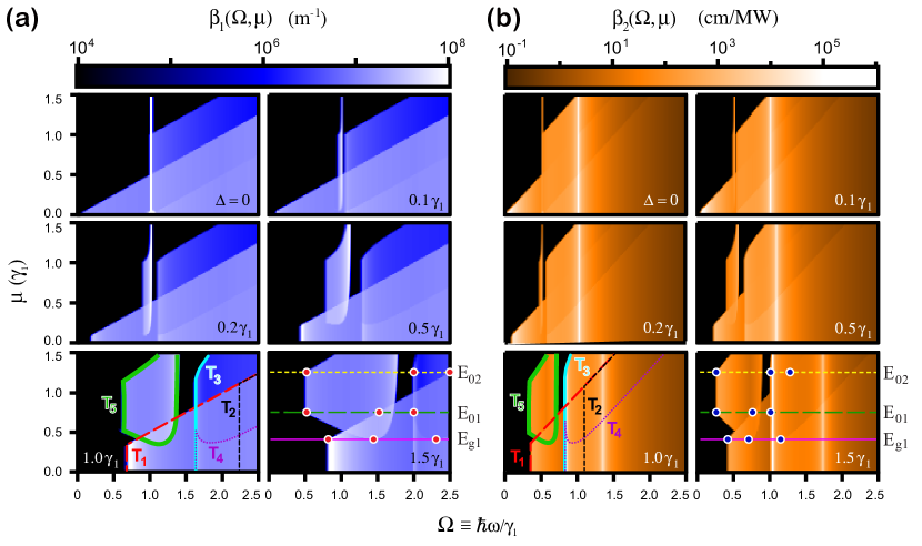
Figure 1 shows the band structure at the -point for a gapped graphene bilayer. The interband 1PA and 2PA transitions are shown, each of which must satisfy the constraints of energy and momentum conservation imposed by the -functions in the expressions for . For the case of 1PA, the thick black arrows in Fig. 1(a)-(d) denote the four one-photon pathways (T1-T4) permitted from for a neutral chemical potential () at a temperature of K. The thick arrow in the fifth panel, Fig. 1(e), illustrates T5, the transition allowed from when .
Associated with each 1PA transition is a family of possible 2PA pathways [30], which are illustrated in Fig. 1 by thin red arrows. In the case of 2PA, two photons are absorbed simultaneously via two energy-nonconserving transitions of and , for which energy is conserved over . For each of the initial and final state combinations, four pathways are possible, all of which are indicated in Fig. 1. The transitions T3 and T4 displayed in Fig. 1(c) and (d) are degenerate. A determination of the criteria imposed on T1-T5 by energy conservation requires the calculation of several important energy values, which are provided for reference in Fig. 1(f) using the nomenclature of Nicol and Carbotte [24] and we shall refer to these values below. We confine our analysis to the case since electron-hole symmetry implies that the response is identical for .
The diagrams in Fig. 1 and the denominator of Eq. (6) allow for several immediate insights into the frequency response of when and . The transitions taking part in the 2PA process for which or , denoted by circular arrows, produce a singularity in at . When becomes large compared to the temperature, this resonance disappears since there are no pairs of initial and final states which satisfy the -function. Similarly, contributions for which produce a singularity at , and 2PA transitions for which give rise to a singularity at . For 1PA when and , a singularity exists only due to T5, which generates an intense, narrow peak at when bands and are perfectly nested. This peak will exist for even when due to thermal population of conduction band and depopulation of valence band .
When an asymmetry gap is present, the conditions imposed by energy conservation become more complex [24] due to the so-called “sombrero” structure [25] of the low-energy bands . The bands are not perfectly nested as they are for , leading to the rich absorptive structure displayed in Fig. 2. Figure 2 shows color plots of both the 1PA and 2PA coefficients for a wide range of gap values. Note that the highest value of is probably unattainable using current experimental techniques, but we wish to display the effects when since several spectral features change. A transformation of accounts for thermal broadening and we take , which corresponds to a temperature of K.
The thermal broadening leads to the emergence in Fig. 2(a) of an intense, narrow peak at due to T5 for (see Ref. [31]). At K, band receives spectral weight due to thermal population, giving rise to T5 transitions of . Similarly, in the spectrum for in Fig. 1(b), the thermal smearing of leads to a peak at , as anticipated during the analysis of Fig. 1. When is small, the divergence in the 2PA is caused by the resonance near the center of the Brillouin zone. This is not present in the 1PA because it is cancelled by the absorption matrix element. When increases, the T5 component of both and broadens into the cleaver-shaped regions outlined in green for in Fig. 2(a,b). The asymmetric broadening of the T5 region is due to the sombrero shape of and the loss of spectral weight when . The panels corresponding to in Fig. 2(a) and (b) identify the energy thresholds mapped in Fig. 1(f), illustrating regions where the chemical potential either blocks or permits absorptive pathways. For , the band gap means that there is no absorption at and the increased density of states at the band edge produces regions of increasing 1PA and 2PA near the T1 cutoff. The other spectrally empty region that emerges with increasing occurs between the T3/T4 and T5 pockets.
In contrast with the requirement of 1PA, 2PA requires , which compresses and shifts the T1-T5 regions in relative to those . Also, Eq. (6) shows that the resonances will be stronger in the 2PA due to the additional factor of in the sum over intermediate states. The spectra for shown in Fig. 2(b) contain a prominent resonance not present in . This resonance, arising at when , is due to transitions T3 and T4, which contain denominators of and give rise to a singularity. As increases, this resonance shifts toward higher due to the increasing size of the band gap. At this T3/T4 resonance, the BLG 2PA strength is several orders of magnitude larger for bilayer graphene than for monolayer graphene [20].
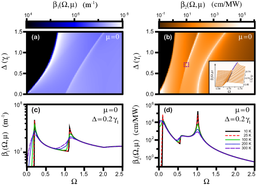
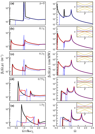
Figure 3 presents 1PA and 2PA curves extracted from the color maps of Fig. 2, grouped by gap value. The left-hand column shows , and the right-hand column shows . For each plot of and , several values of are chosen, each of which corresponds to an identical horizontal line on the accompanying dispersion shown in the inset to the plots. The solid black curves are for ; the dotted red is for which is where the chemical potential is in the middle of the sombrero region; the dashed blue line is for , and lies halfway between and at . When , the dotted red slice is equivalent to that of , so that the solid black and dotted red lines are identical. As , the contributions to of transitions T1-T4 tend to .
Figure 3 reveals an intense, narrow peak in that emerges when , resulting from two routes within the family of T3 and T4 pathways. In particular, routes and lead to a vanishing denominator in Eq. (6) at values of
| (7) |
When and for , the position of the peak, , eclipses the T3/T4 cutoff, causing the peak to appear when the photon energy coincides with and .
Figure 4(a) and (b) show and as a function of and for K and . As increases from , certain regions of increasing intensity materialize in both 1PA and 2PA spectra, including the peak in at , which is outlined in Fig. 4(b) by a dashed purple box surrounding the point . The inset in Fig. 4(b) provides a zoomed-in view of the boxed region, in which the dotted black line indicates the T3/T4 cutoff, and the dashed blue line shows the onset of the emerging peak. Thus far, the assumed thermal broadening corresponds to a temperature of K — a value large enough to reveal the T5 resonance when , yet small enough to avoid the smearing of fine features. Figure 4 (c) and (d) illustrate the effect of thermal broadening on and for at neutral doping (). The most pronounced impact of increasing temperature is the broadening of and into the gap region. Once reaches room temperature, the otherwise abrupt T3/T4 cutoff just beyond spreads into a more diffuse spectral bulge. Similarly, the sharp resonance residing near at K suffers appreciably within the temperature range examined, dropping in intensity by more than two orders of magnitude when K.
We have demonstrated that when an electric field is applied perpendicular to a graphene bilayer, the resulting asymmetry gap gives rise to complex linear and nonlinear optical absorption. This is experimentally verifiable in a simple photoabsorption measurement using transparent gates. For the gapped bilayer system with a tunable chemical potential, we have calculated both one- and two-photon absorption spectra over an expansive range of the gap and chemical potential, taking into account all possible absorption pathways in the calculation of . We analyze the 2PA resonances that emerge in the gapped, doped bilayer system, and examine the evolution of these resonances as a function of and . The effects of thermal broadening are incorporated into the computations, providing insight into the degradation of optical performance at or near room temperature. As graphene-based optical architectures mature, the absorption spectra calculated above will prove important for optimizing and enhancing device performance.
Acknowledgments
This work was supported by Internal Research & Development funds and the Stuart S. Janney Fellowship Program at the Johns Hopkins University Applied Physics Laboratory. MKB thanks Tai-Chang Chiang, Yang Liu, Scott Hendrickson, and Joan Hoffmann for their valuable comments and insight. DLSA is supported by Nordita and by ERC project DM-321031.
References
References
- [1] D. S. L. Abergel, V. Apalkov, J. Berashevich, K. Ziegler, and T. Chakraborty, Adv. Phys. 59, 261 (2010).
- [2] A. K. Geim, Science 324 1530 (2009).
- [3] R. R. Nair, P. Blake, A. N. Grigorenko, K. S. Novoselov, T. J. Booth, T. Stauber, N. M. R. Peres, and A. K. Geim, Science 320, 1308 (2008).
- [4] C. Berger, Z. Song, T. Li, X. Li, A. Y. Ogbazghi, R. Feng, Z. Dai, A. N. Marchenkov, E. H. Conrad, P. N. First, and W. A. de Heer, J. Phys. Chem. B 108, 19912 (2004).
- [5] S.-F. Shi, T.-T. Tang, B. Zeng, L. Ju, Q. Zhou, A. Zettl, and F. Wang, Nano Lett. 14, 1578 (2014).
- [6] D. S. L. Abergel and V. I. Fal’ko, Physical Review B 75, 155430 (2007).
- [7] Hongki Min, D. S. L. Abergel, E. H. Hwang, and S. Das Sarma, Physical Review B 84, 041406 (2011).
- [8] C.-H. Park and Louie, S. G., Nano Lett. 10, 426 (2010).
- [9] M. Liu, X. Yin, E. Avila-Ulin, B. Geng, T. Zentgraf, L. Ju, F. Wang, and X. Zhang, Nature 474, 64 (2011).
- [10] S. J. Koester and M Li, Applied Physics Letters 100, 171107 (2012).
- [11] F. Xia, T. Mueller, Y. Lin, A. Valdes-Garcia, and P. Avouris, Nature Nanotechnology 4, 839 (2009).
- [12] Z. Fang, Z. Liu, Y. Wang, P. M. Ajayan, P. Nordlander, and N. J. Halas, Nano Letters 12, 3808 (2012).
- [13] T. Volz, A. Reinhard, M. Winger, A. Badolato, K. J. Hennessy, E. L. Hu, and A. Imamoğlu, Nature Photonics 6, 605 (2012).
- [14] S. M. Hendrickson, C. N. Weiler, R. M. Camacho, P. T. Rakich, A. I. Young, M. J. Shaw, T. B. Pittman, J. D. Franson, and B.C. Jacobs, Phys. Rev. A 87, 023808 (2013).
- [15] B. C. Jacobs and J. D. Franson, Physical Review A 79, 063830 (2009).
- [16] J. D. Franson, B. C. Jacobs, and T. B. Pittman, Physical Review A 70, 062302 (2004).
- [17] T. Gu, N. Petrone, J. F. McMillan, A. van der Zande, M. Yu, G.-Q. Lo, D.-L. Kwong, J. Hone, and C. W. Wong, Nature Photonics 6, 554 (2012).
- [18] E. Hendry, P. J. Hale, J. Moger, A. K. Savchenko, and S. A. Mikhailov, Physical Review Letters 105, 097401 (2010).
- [19] Q. Bao and K. P. Loh, Nano Letters 6, 3677 (2012).
- [20] H. Yang, Hongzhi, X. Feng, Q. Wang, H. Huang, W. Chen, A. T. S. Wee, W. Ji, Nano Letters 11, 2622 (2011).
- [21] E. A. Henriksen and J. P. Eisenstein, Phys. Rev. B 82, 041412 (2010).
- [22] See, for example, Graphene Nanoelectronics: Metrology, Synthesis, Properties and Applications edited by H. Raza (Springer, Berlin Heidelberg New York, 2012).
- [23] J. Yan, M. H. Kim, J. A. Elle, A. B. Sushkov, G. S. Jenkins, H. M. Milchberg, M. S. Fuhrer, and H. D. Drew, Nature Nanotechnology 7, 472 (2012).
- [24] E. J. Nicol and J. P. Carbotte, Physical Review B 77, 155409 (2008).
- [25] E. McCann, Physical Review B 74, 161403 (2006).
- [26] X. Wang, Y. P. Chen, and D. D. Nolte, Optics Express 16, 22105 (2008).
- [27] The value of for BLG will vary somewhat according to the choice of substrate, which affects only the irradiance prefactor, , in the -photon absorption coefficient, .
- [28] V. Nathan, A. H. Guenther, and S. S. Mitra, JOSA B 2, 294 (1985).
- [29] D. C. Hutchings and E. W. Van Stryland, JOSA B 9, 2065 (1992).
- [30] J. Rioux, G. Burkard, and J. E. Sipe, Physical Review B 83, 195406 (2011).
- [31] For plots labeled , we employed a gap value of in the corresponding computations.