Resonant Landau-Zener transitions in helical magnetic fields
Abstract
The spin-dependent electron transport has been studied in magnetic semiconductor waveguides (nanowires) in the helical magnetic field. We have shown that – apart from the known conductance dip located at the magnetic field equal to the helical-field amplitude – the additional conductance dips (with zero conductance) appear at magnetic field different from . This effect occuring in the non-adiabatic regime is explained as resulting from the resonant Landau-Zener transitions between the spin-splitted subbands.
pacs:
xxxThe experimental realization of an effective spin-transistor remains a challenge facing spintronics since the pioneering concept proposed by Datta and Das.Datta and Das (1990) According to the original idea the operation of the spin transistor is based on the gate-controlled spin-orbit interaction (SOI) of Rashba form.Bychkov and Rashba (1984) The current of spin polarized electrons is injected from the ferromagnetic source into the conduction channel formed in a two-dimensional electron gas (2DEG) and is ballistically transported to the ferromagnetic drain. The state of the transistor depends on the electron spin orientation modulated via the Rashba SOI by the voltage applied to the gate attached close to the channel. The operation of spin transistor has been studied in many theoretical papers. Wang (2004); Zhang et al. (2005); Kunihashi et al. (2012); Wójcik et al. (2014, 2013) However, the experimentsKoo et al. (2009); Yoh et al. (2012) indicate that the signals obtained in the up-to-date realized spin transistors based on the SOI are rather low, which results from the low efficiency of the spin injection from the ferromagnet into the semiconductorSchmidt et al. (2000) and the spin relaxation. The SOI causes that the scattering processes affect the spin states of electrons, e.g., by the Elliott-Yafet or Dyakonov-Perel mechanism.D’yakonov and Perel (1971) Although the spin relaxation is proposed to be suppressed by equating the Rashba and Dresselhaus term,Schliemann et al. (2003); Koralek et al. (2009) the concept of the non-ballistic spin transistor proposed by Schliemann et al. in Ref. Schliemann et al., 2003 is still waiting for the experimental realizations.
An alternative spin-transistor design, with the spin relaxation length as long as 50 m, has been recently described by Žutić and LeeŽutic and Lee (2012) and experimentally demonstrated by Betthausen et al. in Ref. Betthausen et al., 2012. In this approach, the spin control is realized by combining the homogeneous and helical magnetic fields. The latter is generated by ferromagnetic stripes located above the conduction channel. The spin state of electrons flowing through the channel is protected against a possible decay by keeping the transport in the adiabatic regime.Frustaglia et al. (2001) The transistor action is driven by the diabatic Landau-Zener transitionsLandau (1932); Zener (1932) induced by the appropriate tuning of the homogeneous magnetic field. For these suitably chosen conditions the backscattering of spin polarized electrons appears, which gives raise to the large increase of the resistance, i.e., the transistor goes over into the ’off’ state. In contrast to the SOI-based spin transistor, the proposed design is robust against the scattering processes.Saarikoski et al. (2014)
Motivated by the experiment, Betthausen et al. (2012) we have performed
the computer simulations of the spin-dependent transport
in the helical magnetic field for the nanostructure similar to that of
Ref. Betthausen et al., 2012. The calculations of the conductance as
a function of the Fermi energy reveals additional conductance dips,
which cannot be understood in terms of the ordinary Landau-Zener
theory. This effect, not reported in the previous
studies,Betthausen et al. (2012); Saarikoski et al. (2014) is
explained as resulting from the resonant inter-subband transition
between the spatially modulated spin-dependent subbands.
We consider a two-dimensional waveguide (nanowire) in the plane made of (Cd,Mn)Te in the presence of the magnetic field , which is the superposition of the homogeneous magnetic field applied along the -axis and the helical magnetic field taken on in the formSaarikoski et al. (2014)
| (1) |
where is the period of the magnetic field modulation. The Hamiltonian of the electron is given by
| (2) |
where is the conduction-band mass, is the vector potential, is the effective -factor, is the Bohr magneton, and is the vector of Pauli matrices. In the presence of the magnetic field, the - exchange interaction between the conduction band electrons and Mn ions in (Cd,Mn)Te leads to the giant Zeeman splitting of the conduction bands with the effective -factor ranging from 200 to 500.Furdyna (1988)
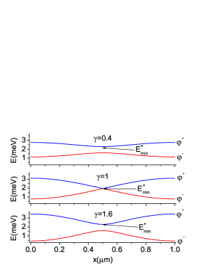
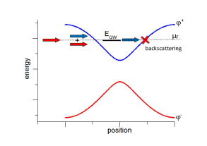
In the superposition of the magnetic fields, the subbands corresponding to the electron with the parallel and antiparallel spin orientation (with respect to the magnetic field) depend on the postion . The spatially-dependent subband energy minima are given by [cf. Fig. 1]
| (3) |
where . Parameter that can be tuned by changing the homogeneous magnetic field determines the spatial modulation of the spin-splitted subbands as depicted in Fig. 1.
We have performed the numerical calculations of the conductance by the tight-binding method on the square lattice with nm using the Kwant packageGroth et al. (2014). In the calculations, the following values of the parameters have been used: the effective mass of electron in CdTe, where is the free electron mass, and . We adopt the hard-wall boundary conditions in the direction assuming the width of the conduction channel nm. The value of the helical magnetic field amplitude has been taken on the basis of the experimental reportBetthausen et al. (2012) and is equal to mT.
The previous studiesBetthausen et al. (2012); Saarikoski et al. (2014) of the spin control in the helical magnetic field have been performed in the adiabatic regime, in which the spin orientation of electrons flowing through the nanostructure follows the spatial modulation of the magnetic field. In the considered nanostructure, the adiabaticityFrustaglia et al. (2001) can be defined by the parameter , where is the frequency of the spin Larmor precession and is the frequency of the magnetic field modulation measured in the electron rest frame, where is the Fermi velocity. In the adiabatic regime, .
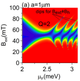
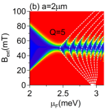
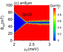
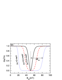
In this paper, we study the spin transport in the regime, in which the adiabaticity condition is weakened. In order to achieve this, we change the period of the helical-field modulation. Figure 2 presents the conductance as a function of the homogeneous magnetic field and the Fermi energy for the different values of corresponding to different . In the calculations, we have considered only the two lowest-energy spin-splitted subbands. The Fermi energy is varied within the range, which ensures that the electrons are injected into the conduction channel from the lowest-energy subband. The conductance as a function of the magnetic field and Fermi energy exhibits the wide minimum centered around the value of helical magnetic field amplitude [Figs. 2 and 3]. The conductance minimum in the range of the magnetic field can be easily understood in terms of the Landau-Zener transitions between the spatially modulated Zeeman splitted energy subbands. The value of depends on the position of Fermi energy with respect to the spatially dependent energy subbands. The mechanism leading to the central wide dip has been explained in details in Refs. Betthausen et al., 2012; Saarikoski et al., 2014.
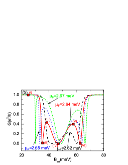
In our study we have found that if the Fermi energy exceeds defined as the minima of the band (see Fig. 1), the additional conductance dips appear for [see Fig. 2(a,b) and Fig. 3(b)]. This effect has not been reported in the previous studiesBetthausen et al. (2012); Saarikoski et al. (2014) and cannot be explained as resulting from the ordinary Landau-Zener transitions, for which the conductance is suppressed only for . The analysis of the conductance maps in Fig. 2(a,b) allows us to distinguish two characteristic features of this effect: (i) the period of the occurrence of the additional dips (measured as a function of the Fermi energy) increases with the increasing period of the magnetic field modulation [cf. Fig. 2(a) and Fig. 2(b)], (ii) the effect disappears in the adiabatic regime (we see that for m () the additional conductance dips are strongly suppressed [cf. Fig. 2(c)]). In order to find the physical interpretation of these additional minima of conductance, we have analyzed six characteristic values of the magnetic field marked by labels (I)-(VI) on the red curve in Fig. 3(b). The chosen values of the magnetic field correspond to the subsequent maxima and minima of the conductance. Figure 4 displays the electron density in the nanostructure calculated for points (I)-(VI).
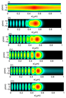
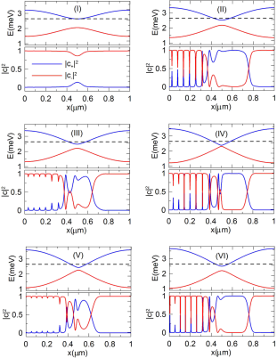
For the case (I) we observe the transmission of electrons through the waveguide with the slight increase of the charge density in the vicinity of the point . At this point the electron transmission is completely blocked in the cases (II), (IV), and (VI). The partial transmission with the non-zero electron density for has been obtained in the cases (III) and (V). Figure 4 shows that the three conductance dips correspond to the backscattering of electrons in the vicinity of . We note that the conductance dips for appear only in the non-adiabatic regime for the short period , which corresponds to . In this regime, the modulated magnetic field, acting on the electron in its reference frame, changes so fast that the electron spin cannot adapt to changes of the magnetic field. This means that the electron, initially injected from the lowest subband , does not remain in this subband when flowing through the nanostructure - the electron quantum state can be described by the linear combination of the eigenstates with the spin orientation parallel and antiparallel to the magnetic field, i.e., by , where and are the space-dependent coefficients. The contribution of each subband is presented in Fig. 5. We see that for the magnetic fields (II), (IV), (VI), i.e., for the conductance dips, the contribution to the wave function in the vicinity of originates only from the subband . Since the electrons are injected into the nanowire in state , related to the lowest-energy subband, one can conclude that the conductance dips correspond to the inter-subband transitions that occur with probability one. On the contrary, for the magnetic fields (III) and (V) the probability of the inter-subband transition is less than one. Although the main conductance dip for [point (IV)] can be easily interpreted in terms of the ordinary Landau-Zener transition,Landau (1932); Zener (1932); Saarikoski et al. (2014); Betthausen et al. (2012) the occurrence of the dips for cannot be explained by the existing theory.
The physics behind this effect can be explained as follows. If the period of the spatial magnetic field modulation is short, the adiabaticity condition for the spin transport through the nanostructure is violated. In this non-adiabatic regime, the state of the electron, initially injected into the lowest-energy subband is a linear combination of the eigenstates with the spin orientation parallel and antiparallel to the magnetic field. This causes that the probability of the inter-subband transition is non-zero. If Fermi energy (the energy of the injected electrons) exceeds , the electrons flowing through the nanostructure experience the effective quantum well created in the spatially varying subband . In this quantum well, the quasi-bound electron states are created. If the Fermi energy becomes equal to the energy of one of the quasi-bound states formed in subband , the probability of inter-subband transition approaches one. This effect, being analogous to the resonant tunneling, can be called the resonant Landau-Zener transition. As a result of these resonant transitions all electrons injected into the nanowire are transmitted to the subband . However, since the energy of the subband in the right contact is higher than the Fermi energy, the electrons are backscattered, which gives raise to the conductance dip. This mechanism is schematically illustrated in Fig. 6.
In order to show that the resonant Landau-Zener transition leads to the conductance dip for , we display in Fig. 7 the conductance as a function of the Fermi energy. The triangles mark the numerically calculated energies of the quasi-bound states in the effective quantum well created in the subband . We see that these energy levels agree very well with the positions of the conductance dips. The results of the extended calculations of the quasi-bound state energy levels as functions of the magnetic field and the Fermi energy are presented in Fig. 2(b) by white dashed curves.
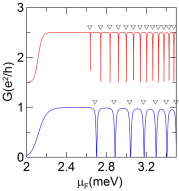
The good agreement between the positions of the conductance dips and the energies of the quasi-bound states allows to conclude that the conduction dips for result from the resonant Landau-Zener transition between the corresponding subbands. We note that the necessary condition for this effect is the non-adiabaticity of the transport (in our case resulting from the sufficiently short period of the magnetic field spatial modulation), because only in this regime the state of the electron is the linear combination of the two eigenstates with the opposite spins. In the adiabatic regime, the electron injected into the lowest-energy subband remains in this state when flowing through the entire nanostructure. Therefore, the probability of the Landau-Zener transitions is zero. This argument explains why the effect presented in this paper disappears for the long period of the magnetic field modulation [see Fig. 2(c)], for which the transport can be treated as adiabatic.
In summary, we have demonstrated that the current flowing through the waveguide (nanowire) made of the magnetic semiconductor in the helical magnetic field exhibits the additional conductance dips for . This effect has been explained as resulting form the resonant Landau-Zener transitions between the spin-splitted subbands that leads to the spin backscattering. We believe that our findings can be important for the spin transistor design based on helical magnetic field. Until now the transport regime in the new design is restricted to the adiabatic regime. We have shown the in the non-abiadatic regime (for the sufficiently small distance between the ferromagnetic stripes) the spin transistor action can be also induced by the resonant Landau-Zener transitions.
This work has been supported by the National Science Centre, Poland, under grant DEC-2011/03/B/ST3/00240.
References
- Datta and Das (1990) S. Datta and B. Das, Appl. Phys. Lett. 56, 665 (1990).
- Bychkov and Rashba (1984) Y. A. Bychkov and E. I. Rashba, J. Phys. C 17, 6039 (1984).
- Wang (2004) X. F. Wang, Phys. Rev. B 69, 035302 (2004).
- Zhang et al. (2005) L. Zhang, P. Brusheim, and H. Q. Xu, Phys. Rev. B 72, 045347 (2005).
- Kunihashi et al. (2012) Y. Kunihashi, M. Kohda, H. Sanada, H. Gotoh, T. Sogawa, and J. Nitta, Appl. Phys. Lett. 100, 113502 (2012).
- Wójcik et al. (2014) P. Wójcik, J. Adamowski, B. J. Spisak, and M. Woloszyn, J. Appl. Phys. 115, 104310 (2014).
- Wójcik et al. (2013) P. Wójcik, J. Adamowski, M. Woloszyn, and B. J. Spisak, Appl. Phys. Lett. 102, 242411 (2013).
- Koo et al. (2009) H. C. Koo, J. H. Kwon, J. Eom, J. Chang, S. H. Han, and M. Johnson, Science 325, 1515 (2009).
- Yoh et al. (2012) K. Yoh, Z. Cui, K. Konishi, M. Ohno, K. Blekker, W. Prost, F.-J. Tegude, and J.-C. Harmand, IEEE Xplore Digital Library 2012 70th Annual, 79 (2012).
- Schmidt et al. (2000) G. Schmidt, D. Ferrand, L. W. Molenkamp, A. T. Filip, and B. J. van Wees, Phys. Rev. B 62, 4790(R) (2000).
- D’yakonov and Perel (1971) M. I. D’yakonov and V. I. Perel, Sov. Phys. Solid State 13, 3023 (1971).
- Schliemann et al. (2003) J. Schliemann, E. J. C, and D. Loss, Phys. Rev. Lett. 90, 146801 (2003).
- Koralek et al. (2009) J. D. Koralek, C. P. Weber, J. Orenstein, B. A. Bernevig, S. C. Zhang, S. Mack, and D. D. Awschalom, Nature 458, 236601 (2009).
- Žutic and Lee (2012) I. Žutic and J. Lee, Science 337, 1225219 (2012).
- Betthausen et al. (2012) C. Betthausen, T. Dollinger, H. Saarikoski, V. Kolkovsky, G. Karczewski, T. Wojtowicz, K. Richter, and D. Weiss, Science 337, 1221350 (2012).
- Frustaglia et al. (2001) D. Frustaglia, M. Hentschel, and K. Richter, Phys. Rev. Lett. 87, 256602 (2001).
- Landau (1932) L. Landau, Physics of the Soviet Union 2, 46 (1932).
- Zener (1932) C. Zener, Proc. R. Soc. Lon. 137, 696 (1932).
- Saarikoski et al. (2014) H. Saarikoski, T. Dollinger, and K. Richter, Phys. Rev. B 86, 165407 (2014).
- Furdyna (1988) J. K. Furdyna, J. Appl. Phys. 64, R29 (1988).
- Groth et al. (2014) C. W. Groth, M. Wimmer, A. R. Akhmerov, and X. Waintal, New J. Phys. 16, 063065 (2014).